Note: Descriptions are shown in the official language in which they were submitted.
- ~ ~20~ 1 54
LSI PACKAGE AND MANUFACTURING METHOD THEREOF
BACKGROUND OF THE INVENTION
The present invention relates to an LSI package in
which large scale integrated circuits (LSIs) for use in
computers and other electronic apparatuses are installed in
high density and a manufacturing method thereof, and more
particularly to an LSI package having a built-in terminal
resistor and a manufacturing method thereof.
In recent years, most of the main functional blocks of
electronic apparatuses including computers above all, other
data processing equipment and communication systems have
come to be incorporated into LSIS to meet the need for ever
faster processing. If LSIs become even larger in the scale
of integration to enable a plurality of functional blocks to
be incorporated into a single LSI chip, wiring between
functional blocks will be shortened to further enhance the
overall processing speed of the apparatus.
On the other hand, available industrial technology
limits the extent of enhancing the scale of circuit integra-
tion and, from the viewpoint of economic optimization, the
plurality of functional blocks constituting an electronic
apparatus are divided into a plurality of LSI chips, which
are arranged in high density to minimize the distances
between them and thereby to increase the processing speed of
the apparatus.
- ~ 22031 54
In particular, what consist of bare LSI chips, not
encased, installed on a small wiring board at minimized
spacing are ~nown as an LSI package (typical of which is a
multi-chip module, abbreviated to MCM). This configuration
is being increasingly applied as a technique to reduce the
wiring distances between LSI chips and thereby to effective-
ly achieve faster processing by electronic apparatuses. One
example is disclosed in Rao R. Tummala et al., Microelec-
tronics Packaging Handbook, 1989, Van Nostrand Reinhold, pp.
786-590.
In such an LSI package, circuits linking LSI chips,
which should ideally be accommodated within the LSI chips
themselves, span the spaces between the LSI chips, and
accordingly are required to permit significantly high speed.
At present, square wave signals of tens to hundreds of MHz
are used for transfers over these circuits.
To drive such LSI chip circuits in an LSI package,
emitter coupled logic ( ECL ) output circuits of emitter fol-
lower type or gunning terminal logic ( GTL ) output circuits
of source follower type, both capable of operating at high
speed and having a large load driving capacity, are used.
In signal wiring connected to such output circuits ( ECL
circuits and GTL circuits), reflection occurs at ends, and
transferred signals are distorted by multiple reflection.
Therefore, in high speed signal transfers, signal wiring
2200 1 5~
should be terminated with intrinsic impedances.
In an LSI package, generally, 10 to 100 LSI chips are
mounted on a wiring board. As the wiring board is rectangu-
lar, having 6 to 15 cm long sides, the signal wiring length
between LSI chips is 10 to 30 cm. Accordingly, when driving
with LSI chips whose pulse rise characteristic is no more
than 1 ns, terminal resistors are indispensable.
According to the prior art, such terminal resistors are
either arranged on the wiring board surface as independent
chips along with LSI chips or formed in advance on the
wiring board as described in the Gazette of the Japanese
Patent Laid-open No. 119047 of 1989 or that of the Japanese
Patent Laid-open No. 227561 of 1991.
As stated above, terminal resistors provided on an LSI
package, according to the prior art, are either arranged on
the wiring board surface as independent chips along with LSI
chips or formed in advance on the wiring board.
As the corresponding area of the wiring board surface
is occupied by the terminal resistance elements in either of
these manners, the distances either between adjoining LSI
chips or between the terminal resistors and input/output
circuits of the LSI chips are extended, resulting in cum-
brance to high speed signal transfers. Therefore, the prior
art involves the problem that the benefit of using an LSI
package in an electronic apparatus (the benefit of increas-
~ 2200 ~ 54
ing the processing speed of the electronic apparatus inwhich the LSI package is used) cannot be fully realized.
An object of the present invention is to provide, in
view of the above-stated problem, an LSI package (LSI pack-
age with built-in terminal resistors), typically an MCM,
which makes it possible to reduce the area of the wiring
board surface occupied by terminal resistors, to position
the terminal resistors close to input/output terminals of
LSI chips and thereby to transfer signals at high speed.
Another object of the invention is to provide a method to
manufacture such LSI packages with built-in terminal resis-
tors.
SUMMARY OF THE INVENTION
According to one aspect of the invention, there is
provided an LSI package comprising: a wiring board whose
main insulating material is either ceramic or glass-ceramic;
terminal resistance elements buried in a direction to pene-
trate said wiring board and formed by sintering resistive
paste consisting of a mixture of fine powder of either
oxidized metal or carbon and fine powder of glass; front
side wiring, formed on the front face of said wiring board
and within the top layer of said wiring board, to connect
the parts of said terminal resistance elements exposed on
the front face of said wiring board to input/output circuits
of LSI chips mounted on the front face of said wiring board;
~ 22001 5~
and back side wiring, formed on the back face of said wiring
board, to connect the parts of said terminal resistance
elements exposed on the back face of said wiring board to a
voltage clamp wiring network.
An LSI package according to the invention may as well
have such a configuration that the constituent elements
mentioned above are augmented with thin-film resistance
elements formed either midway on the front side wiring and
on the front face of the wiring board or midway on the back
side wiring and connected to the terminal resistance ele-
ments either in series or in parallel to be used for trim-
ming of the terminal resistance values.
According to another aspect of the invention, there is
provided a method to manufacture an LSI package comprising:
a terminal resistor array green sheet preparing step to form
terminal resistor array green sheets by printing resistive
paste, which is to constitute terminal resistance elements,
over green sheets composed of the same material as that of
green sheets constituting a wiring board, and drying it; a
green sheet burying step to bury in the wiring board manu-
facturing process the terminal resistor array green sheets,
formed at said terminal resistor array green sheet preparing
step, into the wiring board in a direction normal to the
layer stacking direction of the green sheets in the wiring
board; and a sintering step to bake and sinter the terminal
~ 22 00 1 54
resistance array green sheets, buried into the wiring board
green sheets at said green sheet burying step, together with
the wiring board green sheets.
An LSI package manufacturing method according to the
invention may as well have, in addition to the above-
described steps, a thin-film resistance element forming step
to prepare, by a process of thin-film formation from either
metal films or oxidized metal films, thin-film resistance
elements to be formed on the front face of a wiring board; a
resistor connecting step to connect, either in series or in
parallel to the terminal resistance elements formed in the
wiring board at said sintering step, the thin-film resis-
tance elements prepared at said thin-film resistance element
forming step to a "circuit connecting input/output circuits
of LSI chips to a voltage clamp wiring network": and a
trimming step to trim the composite resistance values of the
terminal resistance elements and the thin-film resistance
elements to the desired terminal resistance values by alter-
ing either physically or chemically either the dimensions or
the electric resistivities of the thin-film resistance ele-
ments.
BRIEF DESCRIPTION OF THE DRAWINGS
Other features and advantages of the present invention
will become more apparent from the following detailed de-
scription when taken in conjunction with the accompanying
- ~ 22001 ~4
drawings, wherein:
FIG. 1 shows a cross-sectional view of an LSI package
which is a first preferred embodiment of the invention;
FIG. 2 shows a perspective view of a partial cross
section of an LSI package which is a second preferred embo-
diment of the invention;
FIG. 3 illustrates a first preferred example of LSI
package manufacturing method according to the invention; and
FIG. 4 illustrates a third preferred example of LSI
package manufacturing method according to the invention.
DETAILED DESCRIPTION OF THE PREFERRED EMBODIMENTS
Next will be described the present invention in detail
with reference to drawings.
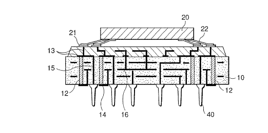
Referring to FIG. 1, an LSI package which is a first
preferred embodiment of the present invention comprises a
ceramic wiring board 10 formed by stacking ceramic green
sheets 11 shown in FIG. 3; terminal resistance elements 12;
front side wiring 13 (wiring formed on the front face of the
ceramic wiring board 10 and within the top layer of the
ceramic wiring board 10); back side wiring 14 (wiring formed
on the back face of the ceramic wiring board 10); through-
holes 15; a voltage clamp wiring network 16; an LSI chip 20;
connecting terminals 21; leads 22; and input/output pins 40.
Although the wiring board in this embodiment is a ceramic
wiring board 10, the invention can as well be realized with
~ 22001 54
a glass-ceramic wiring board. This LSI package has intra-
layer wiring within the ceramic wiring board 10 (however,
the idea of the invention can be applied irrespective of the
presence or absence of intra-layer wiring; the same applies
to a second preferred embodiment to be described below).
Next will be described structural features of this
embodiment with reference to FIG. 1.
This embodiment has structural features (including
operational features) as described in (1) through (4) below.
(1) In the ceramic wiring board 10, consisting of
stacked ceramic green sheets 11, are buried the terminal
resistance elements 12~ The direction in which the terminal
resistance elements 12 are buried in the ceramic wiring
board 10 is the direction in which the ceramic wiring board
10 is penetrated (the direction from the front toward the
back face of the ceramic wiring board 10). The terminal
resistance elements 12 are formed by sintering resistive
paste consisting of a mixture of fine powder of oxidized
metal or carbon and fine glass powder.
(2) One end of each terminal resistance element 12 is
exposed on the front face of the ceramic wiring board 10,
and connected to an input/output circuit of an LSI chip 20
(an LSI chip 20 to be mounted on the front face of the
ceramic wiring board 10) via the front side wiring 13, a
connecting terminal 21 and a lead 22.
-
22001 ~4
(3) The other end of each terminal resistance element12 is exposed on the back face of the ceramic wiring board
10, and connected to the voltage clamp wiring network 16 via
the back side wiring 14 and a throughhole 15.
(4) The LSI chips 20 mounted on the ceramic wiring
board 10 are ECL circuits, and the whole signal wiring in
and out of the ceramic wiring board 10 has dimensions to
make its intrinsic impedance 50 ohms, and the terminal
resistance elements 12 also have a design value of 50 ohms,
though this impedance value is merely one example.
FIG. 2 shows an overhead view of a cross section of the
structure of another LSI package which is a second preferred
embodiment of the present invention.
This LSI package comprises a ceramic wiring board 10
formed by stacking ceramic green sheets 11; terminal resis-
tance elements 12; front side wiring 13; back side wiring
14; throughholes 15; a voltage clamp wiring network 16; an
LSI chip 20; connecting terminals 21; leads 22; and input/
output pins 40. Although the wiring board in this embodi-
ment is a ceramic wiring board 10, the invention can as well
be realized with a glass-ceramic wiring board.
Next will be described structural features of this
embodiment with reference to FIG. 2.
This embodiment has structural features (including
operational features) as described in (1) through (5) below.
22001 54
(1) In the ceramic wiring board 10, consisting of
stacked ceramic green sheets 11, are buried the terminal
resistance elements 12. The direction in which the terminal
resistance elements 12 are buried in the ceramic wiring
board 10 is the direction in which the ceramic wiring board
10 is penetrated. The terminal resistance elements 12 are
formed by sintering resistive paste consisting of a mixture
of fine powder of oxidized metal or carbon and fine glass
powder. This embodiment is the same as the first embodiment
in these respects.
(2) One end of each terminal resistance element 12
(the end exposed on the front face of the ceramic wiring
board 10) is connected, in the front side wiring 13 formed
on the front face of the ceramic wiring board 10, to a thin-
film resistance element 17 formed on the front face of the
ceramic wiring board 10. Thus the thin-film resistance
element 17 is formed "in a position midway on the front side
wiring 13 and on the front face of the ceramic wiring board
10." Incidentally, the position where the thin-film resis-
tance element 17 is to be formed may as well be, other than
the position specified for this embodiment, "a position
midway on the back side wiring 14."
(3) The end of the terminal resistance element 12
connected to a thin-film resistance element 17 as described
in (2) is further connected to an input/output circuit of an
22001 5~
LSI chip 20 via the thin-film resistance element 17, a
connecting terminal 21 and a lead 22.
(4) The other end of each terminal resistance element
12 is exposed on the back face of the ceramic wiring board
10, and connected to the voltage clamp wiring network 16 via
the back side wiring 14 and a throughhole 15. Thus the
connecting terminals 21 pertaining to the LSI chip 20 are
terminated by the series resistance of the thin-film resis-
tance elements 17 and the terminal resistance elements 12.
(5) The LSI chips 20 mounted on the ceramic wiring
board 10 are ECL circuits, and the whole signal wiring in
and out of the ceramic wiring board 10 has dimensions to
make its intrinsic impedance 50 ohms, and the terminal
resistance elements 12 also have a design value of 50 ohms,
though this impedance value is merely one example.
Next will be explained "the presence of thin-film re-
sistance elements 17," a characteristic aspect of the LSI
package which is the second preferred embodiment of the
present invention, as distinguished from the first preferred
embodiment.
The terminal resistance elements 12, buried in the
ceramic wiring board 10, are formed in a so-called thick-
film process, in which resistance paste consisting of a
mixture of fine powder of oxidized metal or carbon and fine
glass powder is printed and sintered. Therefore, their re-
- ~ 22031 ~4
sistance values may deviate from the design value by about
10% on account of manufacturing inaccuracy.
For this LSI package, like the first embodiment, the
intrinsic impedance of signal wiring is 50 ohms everywhere.
Accordingly, in order to transfer square wave signals over
signal wiring of 30 cm or more in length at a frequency of
200 MHz or more, the tolerance of the terminal resistance
should be kept within 1% approximately.
For the first embodiment, to satisfy this requirement
(the re~uirement that the terminal resistance should be kept
within 1~ approximately), the precision of the resistance of
the terminal resistance elements 12 should be improved.
However, the resistance values of terminal resistance ele-
ments 12 are usually subject to deviation due to manufactur-
ing inaccuracy.
By contrast, this (second) embodiment can meet the
aforementioned requirement with the combination of the ter-
minal resistance elements 12 and the thin-film resistance
elements 17.
Thus, for the resistance of the terminal resistance
elements formed by a thick-film process and buried in the
ceramic wiring board 10, a design central value of 44 ohms
is assigned with fluctuations from 40 to 48 ohms tolerated.
Instead, the resistance of the thin-film resistance elements
17 provided on the front face of the ceramic wiring board 10
-
22001 54
is trimmed to between 2 and 10 ohms, so that the errors of
the terminal resistance can be kept within 1%.
Regarding the power to be withstood by the terminal
resistance, 80% or more of it can be borne by the terminal
resistance elements 12 in the ceramic wiring board 10, so
that the thin-film resistance elements need to bear no more
than 20%. Accordingly, in meeting the accuracy re~uirement
as stated above, the area occupied by resistors on the front
face of the ceramic wiring board lO (the thin-film resis-
tance elements 17) can be reduced, and no great area needs
to be allocated on the front face of the ceramic wiring
board 10 for occupancy by the resistance elements.
To add, though this LSI package is superior to the
first embodiments in these respects, the first embodiment
can be fully useful for practical purposes depending on
various characteristic values (including the impedance and
the frequency) of the LSI package.
Furthermore, though the second embodiment described
above has its terminal resistance elements 12 and thin-film
resistance elements 17 connected in series, they can as well
be connected in parallel and the terminal resistance value
set accordingly.
FIG. 3 illustrates a first preferred example of LSI
package manufacturing method according to the present inven-
tion. It shows an overall view of a terminal resistor array
~ 22001 54
green sheet 18 on which terminal resistance elements 12 are
printed and arranged in a row (a green sheet of the same
material as the ceramic green sheets which constitute the
ceramic wiring board 10, which is the main wiring board) and
the manner in which the terminal resistor array green sheets
18 are buried in a ceramic green sheet 11 of the ceramic
wiring board 10.
Next will be described the process of this LSI package
manufacturing method.
This LSI package manufacturing method has the following
steps (1) through (3).
(1) Terminal resistor array green sheet forming step
Before the step to manufacture the ceramic wiring board
10 composed by stacking ceramic green sheets 11, terminal
resistor array green sheets 18, consisting of strips of
resistive paste (the resistive paste which is to constitute
the terminal resistance elements 12) arranged in a row on a
ceramic green sheet 11, are formed in advance (see FIG. 3).
Thus, the terminal resistor array green sheets 18 are formed
by printing the strips of resistive paste, which are to
constitute the terminal resistance elements 12, on green
sheets consisting of the same material as that of the green
sheets constituting the ceramic wiring board 10 (ceramic
green sheets 11), and drying them.
(2) Green sheet burying step
14
- ~ 22001 54
The terminal resistor array green sheets 18, prepared
at the terminal resistor array green sheet forming step of
(1), are buried around LSI chip mounting areas of the cera-
mic wiring board 10 so that the terminal resistance elements
12 be arranged in the direction of penetrating the ceramic
wiring board 10. Thus, in this manufacturing process of the
ceramic wiring board 10, the terminal resistor array green
sheets 18 are buried in a direction normal to the stacking
direction of the ceramic green sheets 11 in the ceramic
wiring board 10.
(3) Sintering step
The terminal resistor array green sheets 18, buried in
the green sheets of the ceramic wiring board 10 (ceramic
green sheets 11) at the green sheet burying step of (2), are
baked and sintered together (simultaneously) with the cera-
mic wiring board 10 (ceramic green sheets 11).
The above-described sequence of steps enables the LSI
package, which is the first preferred embodiment of the
present invention (see FIG. 1), to be manufactured.
In an LSI package manufactured in this manner, one end
of each terminal resistance element 12 is exposed on the
front face of the ceramic wiring board 10 and connected to
an input/output circuit of an LSI chip 20, and the other end
of each terminal resistance element 12 is connected to a
voltage clamp wiring network 16. This arrangement provides
~ 22001 ~4
terminal resistors around each LSI chip 20.
Obviously, the wiring board need not be a ceramic
wiring board 10 but may as well be a glass-ceramic wiring
board. In this case, the terminal resistor array green
sheets 18 should also be made of a glass-ceramic material.
In a second preferred example of LSI package manufac-
turing method according to the invention, the following
processing steps (4) through (6) are taken in addition to
steps (1) through (3) of the first example.
(4) Thin-film resistance element forming step
Thin-film resistance elements 17 (see FIG. 2) to be
formed on the front face of the ceramic wiring board 10 are
prepared in a thin-film process for films of metal or oxid-
ized metal. The thin-film process may typically be vacuum
evaporation or sputtering.
(5) Resistor connecting step
The thin-film resistance elements 17 prepared at the
thin-film resistance element forming step of (4) are con-
nected to "circuits to link input/output circuits of LSI
chips 20 and the voltage clamp wiring network 16" in a
manner of series ("series" here, but may as well be "paral-
lel") connection to the terminal resistance elements formed
in the ceramic wiring board 10 at the sintering step of (3).
(6) Trimming step
Either the dimensions or the electric resistivity of
2 2 0 0 1 5 4
the thin-film resistance elements 17 are altered either
physically or chemically (by grinding, cutting, irradiation
with laser or the like). The composite resistance of the
terminal resistance elements 12 and the thin-film resistance
elements 17 is thereby trimmed to the desired terminal
resistance.
This sequence of steps (4) through (6) makes it pos-
sible to realize terminals of high precision and thereby
enables the above-described LSI package, which is the second
preferred embodiment o~ the present invention (see FIG. 2),
to be manufactured.
FIG. 4 illustrates a third preferred example of LSI
package manufacturing method according to the present inven-
tion.
This example of LSI package manufacturing method addi-
tionally includes the processing of (2') below between the
green sheet burying step of (2) and the sintering step of
(3) of the above-described first or second example.
(2') Flattening step
In advance of the baking of the ceramic wiring board
10, the unevenness of the front and back faces of the cera-
mic wiring board 10, in which the terminal resistor array
green sheets 18 are buried, is removed with a doctor blade
30. Thus, the bulging-out parts of the terminal resistor
array green sheets 18, buried in the ceramic wiring board
~ 2 ~
10, are scraped off with the doctor blade 30 to flatten the
whole front and back faces o~ the ceramic wiring board 10,
in which the terminal resistor array green sheets 18 are
buried (FIG. 4 shows a cross-sectional view of the manner in
which the flattening is accomplished).
The raison d'être of this flattening step consists in
the following respect. To the ceramic wiring board 10 are
soldered LSI chips 20 and various other elements to be
mounted on the surface. For efficient washing after the
soldering, it is desirable for the surface of the board (the
front and back faces of the ceramic wiring board 10) to be
flat. Here lies the meaning of forming a ceramic wiring
board 10 of which both the front and the back faces are
smooth by flattening the two faces of the ceramic wiring
board 10, in which the terminal resistor array green sheets
18 are buried.
As hitherto described, the present invention provides
the following benefits.
The first is the benefit of making it possible to
realize termination in the vicinities of input/output cir-
cuits of LSI chips and thereby to shorten the distances
between terminal resistors and input/output circuits of LSI
chips. The reason for this benefit is that, according to
the invention, the terminal resistance elements are built
into the LSI package in the direction of penetrating the
18
- ~ 2200~ 5~
wiring board.
The seeond is the benefit of reducing the length of
signal wiring to connect LSI chips to one another because
the distances between adjoining LSI chips can be reduced and
accordingly a plurality of LSI chips can be arranged in high
density. The reason for this benefit is that, according to
the invention, terminal resistance elements occupy virtually
no parts of the front and back faces of the wiring board
(since greater parts of the terminal resistance elements are
formed within the wiring board, its surface is scarcely
occupied).
These first and second benefits enhance the terminal
effect of the signal wiring, enable signals to be transfer-
red at high speed, and make it possible to truly realize the
advantage of using an LSI package that "the use of an LSI
package in an electronic apparatus serves to increase the
speed of processing in that electronic apparatus.'~
The third is the benefit of reducing the cost of an LSI
package having terminal resistance elements of the desired
level of precision in the desired number. A reason for this
benefit is that an LSI package manufacturing method accord-
ing to the invention enables terminal resistance elements to
be formed in an inexpensive thick-film process and, more-
over, by simultaneous baking with the wiring board. An
additional reason, regarding the guarantee of precision, is
19
- ~ 22001 ~4
that the second example of LSI package manufacturing method
according to the invention makes it possible to trim the
terminal resistance values with small thin-film resistance
elements.