Note: Descriptions are shown in the official language in which they were submitted.
- W096/09128 2200 1 99 P~l/U~S/11993
~SR FCTiVE REMOVAL OF MATERIAL BY IRRADIATION
Background Of The Invention
This Applic~tion is a Continuation-in-Part of U.S. Pat. App. Ser. No.
5 08/045,165, filed April 12, 1993 (the ~iisclosure of which is i"cGI~.orated herein
by reference and which is referred to herein as the "parent applicalionn), whichis a Continuation-in-Part of U.S. Pat. App. Ser. No. 07/865,039 filed March 31,
1992 (the ~I;;GIQsure of which is i"cGI~orated herein by reference and which is
referred to herein as the ~'039 ~pplic~tion"), which is a Continuation-in-Part of
10 U.S. Pat. App. Ser. No. 07/611,198, filed November 9, 1990, now U.S. Pat. No.5,099,557 (the U-557 ,udlt7nl J, which is a Division of U.S. Pat. App. Ser. No.
07/216,903, filed July 8, 1988, now U.S. Pat. No. 5,024,968 (the "'968 patent").This invention relates to removing material from a surface. More
particularly, the invention relates to the selective removal of material from the
15 surface of a sub~ le by irradiation without altering the physical properties of
material to be left on the substrate that is underlying or adjacent to the material
to be removed.
Effective removal of undesired material from the surface of a substrate is
a critical aspect of many important materials processing and product fabrication20 processes. As described in the parent application, undesired materials (whichmay also be considered as contaminants) include particles, unwanted chemical
elements or compounds, and films or layers of material. Particles may be
- ~ 2200 1 ~9
WO 96~09128 ~ 9S111993
di-~cl~te pieces of matter r~ny; ,g in size from su~"~i rol)s to granules visible to
the unaided eye. Undesil~ad chemicals include any element or compound
which, at the time at which the removal process is performed, is undesit~ble.
For example, hydroxyl groups (-OH) may be a desired r~actiGIl ~ron-oter on the
5 surface of a sul~stldte at one stage of a process and may be an u,-des;.ed
contaminant at s,)~tl,erstage. Films or layers of ,.,ate,ial may be Grydl~ic, such
as human body oil from fingerprints, paint, and epoxy, or i..oryanic, such as
oxides of the sulJ~tldt~ ,nate,ial or other inorganic mate,ials to which the
sulJslrdle has been ex~.osecl.
Such undesired n.ateiials may need to be removed to render the
sub~t,dle more useful for its i"le"ded purpose. For example, in certain pl~cise
scie.)liric measurement devices, accuracy is lost when optical lenses or mirrorsin the devices become coated with l.~icrofi"e surface contaminants. Similarly insemiconductors, surface defects due to minor molecular cor,ld,--inal)ls often
15 render semiconductor masks or chips worthless. Reducing the number of
molecular surface defects in a quartz sel"iconductor mask by even a small
amount can radically improve se".iconductor chip production yields. Similarly,
removing molec~ r surface conta",i"ants, such as carbon or oxygen, from the
surface of silicon wafers before circuit layers are deposited on the wafer or
20 between del,osi~iol, of layers sigf,ifica"lly improves the quality of the computer
chip produced.
Selective removal of layers of the sub~lrdle rnaterial may be done to fQrm
very small-scale structures on the sub~tfdle surface (so-called "nanostructures").
Material (whether suL,:,l,ate material, oxide layers, or other layers of ",aterial)
25 may also be selectively removed in diff~ i"y amounts across the surface of the
sub~t,dte to changes the surface topo$~,dphy ot the subsll~te (such as
smoothing a rough surface).
Material processing equipment often requires treatment for removal of
undesired material to prevent contamination of products processed by the
30 equipment. For example, a significant portion of the undesired material that
ultimately contaminates silicon wafers during production emanates from
~ production apparatus such as process chambers in which the wafers are
placed, quartz wafer boats used to hold wafers for p~ss~ge through quartz
fumace tubes (and the fumace tubes themselves), and pipes that conduct
35 processing gas to the chambers. Accordi. Iyly, the level of wafer contamination
WO96/09128 2 2 0 0 1 q 9 PCI/US9S/11993
e,~.e,ienced during the course of production can be siy-,ificar,lly red~ced by the
periodic cleaning of such apparatus.
In general, any process used for removing material from a sub~t.dte
should do so without at~t:~i,)g the physical prope,lies of the (desired) .nate,ial
that ~3,.,~i..s. The physical properties that should remain l,ndttected can in
ge~)erdl include clystalline stmcture, conductivity, density, dielectric cGI)stanl,
charge density, Hall coefficient, and diffusion coefficient for electrons/holes. In
particular se.,.icond~ctor ~pplicAIions (such as metal oxide semicGI,d~ctor
("MOS"); field effect l,dl,si;,lor (UFEr); and bipolar junction (UBJTn)), the
10 properties can include c~p~cit~nce/area in MOS; junction capacitance; channelcurrent in an FET, directed from drain to source; voltage from collector to base,
emitter to base in a BJT; voltage from drain to source, gate to source in an FET;
MOS threshold potential; MOS surface state charge/area; and storage delay
time. Further, it may be undesirable to change the topos~,~phy (such as the
15 surface roughness) of the remaining material.
As described in detail in the parent ~pplicAIion, many techniques have
been proposed (and are currently used) for removing u"desi,ed materials.
These include wet cl~ernical cleaning (RCA p,wess), dilute HF, ,ne~col)ic and
ultrasonic, and su~er~,ilioal fluid cleaning, UV and ozone cleaning, brush
20 cleaning, vapor HF, laser-assisted liquid cleaning (including the Allen process
and Tam ~r~cess), surface melt, annealing, and ablation.
Another tech"i4ue is plasma c:ea"i"g, which may be used to clean the
process ch~",ber~ of reactive ion etch (RIE) tools after a certain amount of
p,~.cess;"g (e.g. a certain number of wafers) is co",~l~ ted. The prefer,e~l
25 plasma spec.~s are oxygen, carbon tetracl,lolide, and nitrogen, which can be
used in various mass molar CGl)Cen lldliorls for cleaning optics and silicon .
surfaces. Electron cyclol,on resonance (ECR) based plasmas are currently
state of the art. The effectiveness of this type of cleaning is limited to particles --
film removal appears to be difficult and damaging to the electrical parametrics.Dry ice (CO2) cleaning (also known as snow cleaning and CO2 jet spray
cleaning) is a method of delivering CO2 snow via a hand-held device having
various orifices to clean a surface. This technique is limited by the solubility of
the particle in the CO2 snow, e.g. if the particle is not soluble in CO2 then it will
not be removed from the surface. Further, oxides and polymeric films cannot be
35 removed using this cleaning technique.
1~ 22001 99
- WO 96/09128 PCI~/US95/11993
All of these t~cl~ni.~-les suffer from some drawbacks, including: inability
to remove very small particles; undesirable alteration of the underlying
- suLsl,dle's physical ,t~r~ e,lies; consumption of large qua.. lilies of expensive
,..at6.ials such as ultrapure water and gases; and production of toxic waste
5 products (such as HF acids).
Fi!ms, and in particular oX~ Gll films, are a cOI~ Ol1, troublesome
c~le~oly of mdl~lials that need to be removed from a suL~tl~dte. Most ,.,alerials
that are q.~ osed to an oxy~enated ~l-,)Gsph6re (e.g., air) form a native oxide
that coats the surface. Such oxide layers are typically a s~ .lially
10 continuous Iayer of molecules of the oxide l,.atelial. In most cases, this native
oxide layer is del,i..)e.ltal depending on how the suL,~t,~te material will be used.
One approach to this problem has been to maintain the su6-~l,dte material in a
vacuum to prevent oxide growth. Known techniques for removing oxide films
include treating them with strong acids such as aqua regia, sulfuric acid and
15 hydrofluoric acid.
In se...ico~"~uctorfab~icdlion, the removal of native oxide (silicon dioxide)
from the silicon sul.~l,ale is of great COnC61ll as tecl~no'o3y geomet.ies
continue to get smaller. Current l--ell-ods to remove the silicon dioxide employliquid HF, and ex~.eli...enls are being undertaken with vapor phase halogens
20 and vapor phase l-alogel-s in conjunction with UV radiation. B. Van Eck, S.
Bhat, and V. Menon, ~Vapor-phase e~cl,;ng and cleaning of SiO2,n Proceçdin~s.
Mic~oconta,),i.,alion 92. (SantaClara, CA; October27-30, 1992), p. 694; J. de
Larios, W. Krusell, D. McKean, G. Srn~l;, .shy, B. Doris, and M. Gordon, ~Gas-
phase cleaning of trace metal and organic contaminants from wafers:
25 Ultraviolet irrAdi~ted oxygen-based and chlorine-based chemistries,"
Proceedings. Microconta"lination 92. (Santa Clara, CA; October 27-30, 1992)
p. 706; M. Miyashita, T. Tusga, K. Makihara, and T. Ohmi, ~Dependence of
surface microroughness of CZ, FZ, and EPI wafers on wet chemical t)rwess;,.g,"
Joumal of the Ele~,1,ocl)emical Society. vol.139 (8) 1992, p. 2133; and T. Ohrni,
30 UULSI reliability through ultraclean processing," Proceedings IEEE. vol. 81 (5),
p. 716. Using halogen-based chemistry can damage adjacent circuitry since it
is a gross, rather than pinpoint, method of removal.
Removal of surface oxides is also important in preparing metal suL,~l.d~es
for the ~pplic~liGI~ of adhesives as an altemative to welding in aerospace,
35 automotive and construction (building) applicalions. Removal of oxide films
WO96~09128 22~ 1 99 ~ u~ l993
also has a~ tions in reconditioning weathered metal surfaces and improving
the grade of circ~ t~ coinage.
Another i!"~Gna"l ll~dllllel)t pr~cess is the credliol) of "-anostl-lctures
(e,.l,~",ely small physical structures) on or in su6st,dte materials, such as
5 pressure trans~ucers, A~colel~n,eters, atomic force ,~,icrùscoue probes, and
micr~r"otor-~. One technique ~,r,posed for cr~dliG" of l,ano:jt"~ctures involvescl,emloal et :llillg in combination with masking techni~ues (useful in bulk
l,.icr~l"acl,i.ling where structural layers of n,ale,ial are built upon a wafer and
then a sac,iricial layer is etched away). J. Bryzaek, K. rele,~on, and W.
10 McCulley, IEEE Spectrum. May, 1994, p. 20. Another proposed tecl,l,iq-le
involves the laser-focuse~ deposition of material. J.J. McClelland, R.E.
Scholten, E.C. Palm, and R.J. Celotta, "Laser-focused atomic deposition",
Science. vol. 262, 5 November 1993, p.877.
Another important treatment process is planarization, to eliminate or
15 reduce non-u"iro""ilies in the surface of a su6stldte. A commonly-used
technique for planari~dlion is chemical mechanical polishing (CMP), which uses
pr~p,ie~dry slur~ mixtures to grind the surface to a planar level through the use
of polishing pads. This surface polishing provides the advantage of improved
chip performance. CMP plandri~dlion is conl,ulled by "etch stopsn and by timing
20 the pr~cess so that e~essive polishing does not occur. This prûcess produces
large quantities of contaminants (residual from the slurry) and is very expensive
(with an average cost of appr~xi",ately $35 per wafer), which is attributable tothe cost of the consumables such as slurry, water, pads, and brushes for brush
cleaners. Another problem ~ssoc;~led with CMP is removing the slurry rccidu~l
25 from the wafer surface. Removal using brush clea.,i"y, which is the current
prucess, is only ertici¢nl to approxi",ately 0.5,um particles. An ~d~iitional
~ l,aclc of the CMP planari~alio" pi ocess is that it is not clusterable with other
current cleàning technologies.
Summary Of The Invention
The invention soives the problems and avoids the drawbacks of the prior
art by selectively removing undesired material from a treatment surface of a
subsl~te by irradiating the undesired material with energetic photons having a
spatial and temporal conce"l,~lion (energy and power fluxes) sufricient to
remove the undesired material and insufficient to alter the physical properties of
35 the underlying sub~ dle. Preferably, a gas is flowed continuously across the
WO 96/09128 2 2 0 0 1 9 9 PCI/US95/11993
surface to carry away removed material to avoid redeposi~;n~ the material
elsewhere on the l,eal,n~,ll substrate. Optimaily, the gas is inert to the suL,~lrale
and to the n,ale,ial to be removed. Moreover, to best avoid the ,uosc;' ility ofcontaminants ~ dille~l in the flow being deposited on the tr~al",e"t surface,
5 the flow of gas is ~r~f~rdl~ly in the laminar flow regime.
The I~J;~liG,, source (of energetic pholons) may be any means known in
the art to provide photons of the requisite energy level, including pulsed or
continuous wave lasers and high-energy lamps. In some applic~liGns, such a
those in which the bonds of interest require the near-simultaneous ~pplic~lion
10 of multiple photons, a source with a high power output is preferred, such as a
pulsed ultraviolet laser.
The invention is shown to be applicable to the removal of substantially
continuous layers of undesired organic and inorganic films. Removal of organic
films includes removing paint and marker from stainless steel or quar~7
15 substrates. Removal of inorganic oxkJ~lion films includes removing oxid~tion
from chromium, molybdenum alloys, nickeUiron alloys, stainless steel, tantalum,
tu"g~len, copper, erbium, and zirconium and removing polycrystalline silicon
from quartz. Depe"cl;. -~ on the pro,u~, lies and thickness of the undesired
material and the subslldle, and the properties of the available radiation source,
20 it may be "ecess~ry to remove the u"des;,ed material in a succession of
treatment ~pl)lic~ )s.
The topography of a surface may also be modified by apprl,priale
~pp'i~tion of the treatment process. For example, relatively more material can
be removed for reyions in which the thickness of the ".ale,ial is relatively
25 greater, and less in regions where the thickness is less to produce a more
unifomm material thickness. This can effectively reduce the surface rouyl ")ess of
the material. A source of photons can be coupled in a control loop with an
elli~,sG,neter or other surface metrology device to provide feedback to monitor
and control the removal of the material in each region. Similarly, applying the
30 radiation to a rough surface at a relatively shallow angle provides a greaterincident conce"lr~lion of photons on the more prominent portions of the surface,while the less prominent portions are shadowed and thus receive a lesser
concerllrdlion of photons. Relatively more mat6,ial is therefore removed from
the prominent portions, reducing the surface roughness.
Nanostructures can be created by selectively irradiating a surface to
remove material from selected areas to a selected depth.
WO 96/09128 2 2 0 0 1 9 9 f ~ /L~/11993
Brief Description Of The Drawings
Fig. 1 is a scher"~lic diagram of a method and appardl~s for removing
desil~d n,ate,ial from a substrate according to the principles of the invention.Figs. 2A-B are scl,e,-,dtic diagrams of two test apparatuses used to
5 remove ,.,al~;,ials from se'ecte~ substrates.
Fig. 2C is a s-:he",~lic ~ gldnl of a third apparatus, similar to those in
Figs. 2A-B but with a simpler optical train.
Fig. 3 is a schematic ~iayr~ of the geometry of the i,lcide,lt rA~;~tion
region produced on a sul~:jlr~le by any of the apparatuses of Figs. 2A-C.
Fig. 4 is a schematic illustration of a technique for selectively removing
material from a sul.:jl,dte to create nanostructures.
Fig. 5 is a schematic illustration of a substrate prior to the process of
planarization.
Fig. 6 is a scl)en~dlic diagram of a first apparatus for use in the process of
15 plana,i~dlion of the suL,slldle of Fig. 5.
-Fig. 7 is a s~;l,ematic illu:~lr~liOl) of the selective red~Jction of the surface
roughness of a sul,:jlldte by i"ddialil)g the surface ohli~uely.
Detailed Description
R~r~r~nce will now be made in detail to presel,lly preferred embodiments
20 of the invention, examples of which are illust~dled in the accG",pa"ying .
drawings. Throughout the ~ d~;ll9S, like r~ter~nce characters are used to
designale like elen)ents.
1. Basic Treal",ent Method and Apparatus
A ",ethocl and apparatus for removing undesiled material from a
25 llaall"ent surface of a substrate without altering the physical properties of the
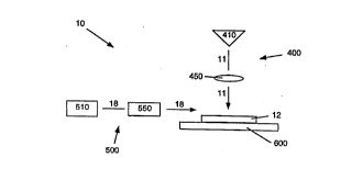
su~slldle is illustrated sche",alically in Fig. 1. As shown in Fig. 1, apparatus 10
for treating a substrate 12 from which undesired material is to be removed
includes a radiation system 400, a gas system 500, and a relative motion
system 600. Irradiation system 400 includes a source 410 of radiation 11
30 (which consi~ls of energetic ~.hotons), such as a laser and suit~h!e deliveryoptics 450 that conduct radiation 11 to the treatment surface of su~sll~le 12.
Gas system 500 includes a source 510 of a gas 18 and an ~ssoci~d delivery
system 5~0 for flowing gas 18 over at least the portion of the surface of suLsl,dte
~WO 96/09128 2 2 0 0 1 9 9 PCr/US95/llg93
12 to which rAdiation 11 is applied. Gas 18 is preferably inert to sub~t,dle 12
and is flowed across sub~t,d~e 12 so as to bathe sub:jl,dle 12 in a non-reactivegas env;r~.,..,enl. Preferably, gas 18 is a chemically inert gas such as helium,r,itluS~6r" or argon. Relative motion system 600 provides for relative motion
5 l~et~l on a portion of the l.edl."e,lt surface of sul.~l.dte 12 to be t-ealed and
Prl;~tion 11 a~id, ~tiGIlally, gas 18.
Each of the constituent ele",el,ls of these cGi"~.one,)ls of apparatus 10
(P~ tion source 410, delivery optics 450, gas source 510, gas delivery system
550, and relative motion system 600) may be such as are deso,il,ed in the
10 parent a,~)plicalion and are readily select~hle by the artisan to configure the
apparatus in accor~ar,ce with the principles of the invention. For example,
delivery optics 450 may include mirrors, lenses, optical fibers, collimators,
apertures, and other elen,enls. Gas delivery system 550 may include conduits,
chambers, lines, valves, filters, flow meters, and other elements. Relative
15 motion system 600 may be any suitable system for l,d,)sldliooal or rotationalmovement of sul,sl,dle 12 with respect to radiation 11 and gas 18, and may
include a t,dnsldlional stage for planar tldnsldliGI) of the sul~l,ala, a ~otdtiGI)al
fixture for r~lali"g the sub~ dle, or movable co",po"ents in the delivery optics to
scan rA~;~ffon beam 11 across the sul~ dla. Illustrative embodi",e,lls of
20 apparatus 10 are desc,ibed in more detail below.
AccGrdi,l~ to the method of the invention, energetic ~)I)ùtol,s are
irrA~i~ted upon the suLsl,dte lr~",enl surface in a spatial and temporal
conce,)l,dliûn (energy and power fluxes) sufficient to remove undesired materialfrom the su~sl,ate l~al",enl surface and insufficient to alter the physical
25 properties of ",ate,ial that is cles;,~d to be left on the s~ tld~e surFace.
To remove the ul~desi,ed mai6r;al, the bonds by which it is adhered to the
underlying and ~ cent ",al~lial on the treatment surface (which may be more
of the same material, the su6~ dle ",alerial, or a third material) must be broken.
Each such bond is broken by introducing an amount of energy at least equal to
3û the energy of formation of the bond. Bond fommation energies (i.e., the amount
of energy released when the bond is fommed) for common substrate materials
are shown in Table 1 a, below. The bond energies shown are between the
material eler,lel~ls themselves (e.g., Cr-Cr) and between the material element
and oxygen (e.g., Cr-O). Bond formation energies for various carbon
35 compounds are shown in Table 1 b, below.
22001 99
- WO 96/09128 PCT/US9S111993
,,
Tabl~ 1a
Bo ~ Furnabon ~ry (eVhond)
r~ oxna~ (~)
C . . A~_
Fe . "
Nl .
~r
la
W
Tabl~ 1b
C ~
Cl .,
~o
~..
Zr
5 The bonds are broken wh~en energy carried by ~ olo,~s is imparted to the bondsin an amount greater than the bond fommation energy. It is be'ievcd that there
are energy inefficiencies inherent in this bond-breaking process and, therefore,that the amount of photon energy required is approxi",ately twice the bond
fommation energy. As can be seen in Tables 1a, oxide bond energies are on the
10 order of 4.0 to 8.3 eV, while orya,)ic (carbon) bond energies are on the order of
3.5 to 11.2 eV. Thus, photon energies of appr~)~i",alely 7 to 22 eV are required.
- The energy of a photon depends on its waveleny~l" in the relaliol-slli,u:
E hc
= _
where c is the speed of light (3.00 x 10⁸ m/s), ~ is wavelength (m), and h is
15 Planck's cons~al~l (4.14 x 10⁻¹⁵ eV sec). Selection of the source of photons
therefore depends on the photon energy required, and thus on the wavelength
required. A variety of lasers are identified in Table 1c, below. The table
identifies the laser medium (and whether the medium is gas (g), liquid (I), solid
(s), or plasma (p)), the photon wavelength ~ (nm), and the photon energy Eph
20 (eV). For continuous wave lasers, an average power PaVe (W) is also shown,
and for pulsed lasers, the energy per pulse EpUlse (J). a representative pulse
duration tpUIse (ns) and the peak power during a pulse Ppeak (MW).
WO 96/09128 2 2 O O 1 9 q P~ 5~11g93
.
.~ .
Table 1c
M~Un A ~Ph ErLISe tPUI~ C PaVe POeak
(nm~ ~~ ) tnS ~U~
C (6-) (P) . ~. E~ 4. ~E_~
A~C~XGTer(q) .~ E- 1.C~E+_
KC~YCner(~ .V .~ E- ~ 1.4 E+~
HJ~ ) ~ ~ 1.1 E~
A t (C)
n 1 ~ ' ~ 6G dye (~ E~
~V .~ E-
H~ e (q) _~ . . E~
Kr+ q ~~ . . E-
RUbV S) .5.00EIOO 50 1.00E+O2
~(3+)'A~O3 (S) 1.00E+O1
C (3+ :~laSS (S) ~ . 5.00E+O1 50 1.OOE+O3
~(3+ :YAG (S) ~ . ~~E+
Co Or Center (S) . ~ . -
*_ . .
H~Ne (q)
FEL (LANL) ~ .l .OOE-03 60 2.00E-O2
~ ~r . 1.00E-03 50 2.00E-02
:O ~ +
-2C ~ E~
- _ . - C~ 3_ . ~ 4 .~ E~
Comparing the photon energies for the above lasers to the required energies
ide"liried above for common suL)~ te materials (and accounting for the
5 expected inefficiencies), it is apparent that in most cases the energy of a single
photon will not be sufficient to break the bonds of i"lerest. However, it is
believcd that the bond-breaking energy can be supplied by multiple photons if
the photons strike the bond within a very short time, or esse"~ially
'tsimultaneously.n
Since a certain amount of energy is required to break each bond, the
total amount of energy (and thus, the total number of photons of a given energy)required to remove a given amount of undesired material from the treatment
surface of a suL,- trdte is generally proportional to the number of bonds in that
amount of material. It is believed that photons interact with bonds only in the
15 interfacial region of the treatment surface (i.e., the topmost one or two layers of
atoms or molecules (monolayers)). For removal of substantially continuous
layers of material (such as oxide layers) it is therefore helpful to consider unit
surface areas and thicknesses of material in monolayers. Thus, for a given
surface area, the removal of a certain thickness (or number of monolayers) of
20 material requires the effective application of a given amount of energy (number
of photons). Of course, not all of the photons that strike a subsl,ate treatment
WO 96/09128 2 2 0 0 1 q 9 PCI~/US95/119g3
surface will co"l,iLute to bond breaking -- it is believed that a small ~Id;tion of
the photol,s co,llli~ute to bond breaking. This is believed to be at least in part
bec~use the effective localions (the bonds, or parts thereofl for absorption of the
photon energy occupy a small fraction of the surface area. I low~vcr, at least for
5 a given material, it is believed that there is a relatively col)~lant r~31dliGI~ship
l~l~ren the actual number of photons required and the ll,eGr~lical number
based on the number of bonds to be broken. Accordingly, a relevant parameter
to consider is the energy flux (energy per unit area, or number Of t~l ,oto"s per
unit area) applied to a subal,~te treatment surface, which cG"e~ponds to a
10 thickness of undesired ",ateiial removed.
As noted above, there are cases in which the bonds of interest require
more energy than is carried by a single photon emitted by the selected radiationsource. Such bonds are referred to herein as a Umulti-photon bonds." As noted
above, the energies of two or more photo"s are believed to be additive to
15 supply the energy required to break a multi-photon bond only if the photons
strike the bond simultaneously. This i"~plicAles the arrival rate of photons at a
bond site, which is a power flux (energy per unit time per unit area). Further, it is
b~l evcd that there is a probabilistic nature to multi-photon bond breaking. For a
given average power flux over an area of the sub:jlr~te, there is an average
20 arrival rate of pl ,~tons at any given bond site. However, the actual arrival rate of
photons should be ra"dG"~ly distributed about the average value. Thus, if there
is a minimum photon arrival rate (maxi",um time interval bt:t~rccn the ,uhoto"s)at which photon energy ~ddition will take place to allow breaking of a multi-
photon bond, an average power flux ~pplied to a given area that CGI le~pGl)dS to25 that minimum arrival rate will ex~.ose a~,pr~xi",ately half of the bond sites in that
area ex~.osed to the req~isite arrival rate (or a greater rate). Conversely, even if
the average power flux is somewhat lower than that required to produce the
minimum required photon arrival rate, it is expected that photons will arrive atsome of the bond sites within the required interval.
In summary, to remove a given thickness of undesired material from a
substrate treatment surface, a minimum total energy flux (a total number of
photons of a given energy level per unit area) must be applied to the undesired
",dlerial. If multi-photon bonds are involved, a certain power flux is also
required, and the higher the power flux, the greater the chance that each bond
35 site will be subjected to the requisite photon arrival rate. The selection of a
suitable source of energetic photons thus requires an evaluation of the required
WO 96/09128 2 2 0 0 ~ 9 ~ PCIll~S95/11993 ~ -
photon energy and, for multi-photon bonds, the available power. As will
l~ecome apparent from the data presented below, to remove oxides and or~anic
films (which have high, and therefore multi-photon, bond energies), ~.rt:~"~d
photon sources are U~er~r~ pulsed UV lasers, which have the l.i~l,e~t peak
5 power levels and high photon energies.
A cor..~x~ti. .~ considef~lion limits the energy and power fluxes that may
be a~ d to a sul,~ te l,ealloenl surface - the need to avoid altering the
physical ~orol~e,lies of the ~ale,ial that is to be left on the surface. In general,
changes in the physical properties of a .nalelial are c~llsed by increasing the
10 temperature of the material above a tl.reshold level. The change in temper~lure
of the surface of a n.ate,ial caused by the application of radiant energy depends
on the heat transfer characte,i~lics of the material and the power and energy
fluxes of the Appliecl radiation. Finding the maximum power and energy fluxes
usable on a given su~st.dle ,..~le,ial will require some ex~eri..,enlalion. Prior
15 art laser cleaning tecl,ni-~ues that rely on vapori~dlion, ablalion~ or surface
melting provide some guida..ce in the energy and power fluxes required to
produce state cl.anges~in su~sl-ate materials.
In general, the ,~I.olons are pr~fer~bly dif~oted pe.~e..dicular to the plane
of the portion of the sul,st.~te being treated, to maxi...i~e the power and energy
20 fluxes at the surface for a given output from the source of ~hotons. I lowevcr, the
photons may be di.~ d at an angle to the sul,~l.dle as convenient or
necessAry for implen-~nldlion of the process in a particular envir~ l"el)l. Of
course, the energy and power fluxes at the surface will vary with the sine of the
angle of i-.oidence of the f~l)oto,)s with respect to the plane of the surface, which
25 must be taken into account in selecting the output of the photon source. In some
~it~Ations, it may be p,~r~ble to direct the radiation at an ohli~lne angle to the
suL,stlat~ to ,or~fer~--lially irradiate, and thus remove, peaks in the material to
smooth it.
2. Test Apparatus
Two sets of test apparatus (referred to herein as apparatus A and B) were
used in the following examples. Apparatus A is illustrated schematically in Fig.2A. In this apparatus (identified in the figure as 10A), the radiation source islaser 411, which is a pulsed KrF excimer laser, sold by Lambda Physik as
model number LEXtra 200. This laser has a wavelength of 248 nm (for a photon
energy of 5.01 eV), a maximum output energy per pulse of 600 mJ, and a fixed
WO 96/09128 PCI/US95/11993
22001 99
13
pulse duration of 34 ns (for a maximum power per pulse of 17.65 MW). The
..,a~i.~.um pulse repetition rate is 30 Hz producing a maximum average power
of 18 W. The rAr~;~tion beam is 23 mm by 13 mm at the laser output.
Radiation delivery system 450 includes in the order encountered by
5 r~dialiGn beam 11 upon leaving laser 411, an aperture plate 452, 45~ tuming
mirrors 453, 454, 455, and 456, and ~ ust:3hl~! focusing lens 457. Aperture
plate 452 is a flat plate with a rectangular aperture 6 mm wide and 25 mm long,
and is used to block the Utails" of the f~ ssi~n distribution of ,~I ,otol~s ema"dli"~
from laser 411, so that the spatial distribution of energy in radiation beam 11 is
10 appr~xi..~ately uniforrn across a plane perpendicular to the beam. Each of the
tuming mirrors 453 and 454 are 50 mm, and 455 and 456 are 25 mm, planar
mirrors. A~just~hle focusing lens 457 is a cylindrical lens with a width of 25 mm
a length of 37 mm, and a focal length of 75 mm. By selecting the height of
focusing lens 457 from the surface of su6slr~te 12 and the orientation (concave
15 side up or down~ of the lens the width of the beam spot at the su6st,~e surface
is ~ljusted All optical elements are anti-r~lectiol1 coated for 248 nm light.
The delivery system 450 of the seco, -d apparatus, Apparatus B (shown in
Fig. 2B), is ide, Itical to that of Apparatus A except that first tuming mirror 453 is
omitted (and laser 411 and aperture plate 452 are co,.~spo,.dingly reoriented
20 90~ to point directly toward tuming mirror 454) and tuming mirror 455 is 50 mm
(rather than 25 mm as in Apparatus A). A third apparatus (not used in the
e,~.e,il,~ents) with a si,..~lEr (and therefore ~,r~r,ed) optical train is shown in
Fig. 2C.
RAdi~tion beam 11 is delivered a,uproxi"~ately pe".en~i ular to stage
610 on which suL,~;~,dte 12 is mounted. As shown in Fig. 3, stage 610 can be
l,anslaled in the X and Y ~ ;tiGns (parallel to the plane of the stage, and
in~licAted in Fig. 3 by arrows X and Y). R~ tion beam 11 produces a generally
rectangular incident radiation region 611 with a width w and a length 1. Region
611 is swept across the surface of su6sll~la 12 by translating stage 610.
Gas delivery system 500 inciudes a dewar of liquid nitrogen (4500 1
capacity) coupled in series to: a dual stage regulator; a moisture/oxygen
adsorber (MG Industries Oxisorb which adsorbs to concer,l,~lions of 0.01 ppb);
a Millipore Model 304 particle filter (filters to 0.00311m); a flow meter; a U.S.
Filter Membralox filter (filters to 0.001 llm); and thence to a nozle 551
te""i, lalil ,g adjacent region 611. Nozle 551 discharges a flow of gas 18
across region 611 and remains fixed with respect to region 611 so that stage
W096J09128 220079~ S~Il993
14
610 and sub~ldle 12 l.d"slate with respect to it. This gas delivery system is
useful for male,ials that are not sensitive to typical al,l.ospheric gases, and
per,l,ils a simpler apparatus than is required when it is required or des;.ed toisolate the sulJalldla from the dl",osphere during l,~al",en~ (such as ~I;;clQsed in
5 the parent application).
A video C~ erd 700 iS po-~;ilio,led to view region 611 and thus provide
visual data on the results of lledlll1enl.
In the illu tldled embodiment, stage 610 is first llculslated longitudinally in
the X dil~ctio~, as r~iztion beam 11 is applied to the surface of sul~ te 12,
10 producing an elongated rectanguiar swath 612 on suL,:jlr~e 12 that has been
exposed to r~di~tion beam 12. Stage 610 may be indexed back to a starting
position and l,d"slated in the X direction again so that radiation beam 12 makesanother "pass~ over swath 612. After one or more p~Cses~ stage 610 may be
l,anslated laterally in the Y direction a ~i~lal)ce appr~xi,nal-~ly equal to length /,
15 then l,a"slated again through the X ~JilwtiGn to form another swath ~r~j-cent to
the previous swath 612. Thus, the portion of the surface of sub~t,dte 12 to be
treated is sequentially exposed to rA-P~tion beam 11 and the concurrent flow of
gas 18.
The energy flux (energy per unit area) applied to any point on the surface
20 of sUbSl,dle 12 by r~ tion beam 11 during a single pulse of laser 411 is equal
to the energy of the pulse at the surface divided by the area over which that
energy is distributed. This can be expressed as:
F - EPS
ep / w
where FepS is the pulse energy flux per unit area at the surface (J/cm2), Eps is
25 the pulse energy at the surface (J), ànd / and w are the length and width of
region 611 (cm). Similarly, a pulse power flux (Fpps) can be c~lcul~ted as:
F _ FePs
PP tp
where tp is the laser pulse duration.
There are energy losses associated with the passage of radiation beam
30 11 through the optics and aperture plate. Thus, the laser pulse energy at thesurface (Eps) is less than the emitted laser pulse energy. The LEXtra 200 laser
includes a mini-controller with a pulse energy meter that is useful for recording
~WO96/09128 22 0 U l ~ ~ PCT/US95/11993
the laser energy output during experiments. However, the intemal meter is not
e~ "ely accurate. To provide more accurate energy measu,~n,ents, the test
apparatus was calil,r~led to develop a corr~ction factor to be applied to the
intemal meter reading to produce a more accurate reading. Accordingly, the
5 laser pulse energy at the surface (Eps) was measured with a 1~ ctron J50
dett,ctor head and JD 1000 joulemeter ~ )osed at the localiG" of the t,.3at~"e,
surface, and the measured energy reading compared to the intemal meter
reading of pulse energy (Epm). A co~e.:tiGr, factor (RCGr.~ n) was thus
dcveloped that included both the losses through the optical train and the meter
10 inaccuracies.
EpS = Epm RCo~ection
This cot,ection factor is not constant -- it has been found to vary a~proxi",ately
linearly with the output level of the laser. The pulse energy is dependent on the
voltage input (Vl) to the laser which can be adjusted to levels between
15 approxi",alely 17 and 22 kV. The laser output energy (as i"d;cated by the
intemal meter) varies for a given voltage setting depe"di. ,9 on such factors asthe laser gas supply level, so that the voltage cannot be used directly as a
measure of pulse energy, but instead the intemal meter is read. For
convenience, the correction factor is c~lcul~ted as a function of the voltage
20 setting, then ~pplied to the energy read from the internal meter. The correction
factor is of the forrn:
R _ 1
cor,~ctiG~ m . Vl + b
where m is the slope, and b is the intercept of the linear relationship.
The values of the m and b for the two test apparatuses are shown in
25 Table 2a below.
Table 2a
Factor Ap,o. A App. B
b 1~0 0.74
m o.a29 0.066
Thus the energy per pulse at the treatment surface is:
E _ EPm
ps -
2200 ~ 9~
WO 96/09128 PCI~/US95/11993
16
In the illustrated embodiment, a swath 612 is fomled from a series of~liscr~le regions 611 (as indicated in Fig. 3 by a second region 611 shown in
phanlo",). The Ji.,td"ce by which region 611 is offset from region 611 (~X) is
the product of the time b~t~r~en laser pulses (which is the inverse of the laser5 pulse .epeti~;ol~ !ate Rd and the velocity of transldlion of stage 610 (the scan
velocity vS). The energy flux delivered to a given point on the subs~.dte is thus
the product of the energy flux per pulse (FepS) and the number of laser pulses
to which the point is e~l~os~.~ (Npl). The number of pulses Npl is equal to the
width w of region 611 divided by the dislance ~X that the stage moves bel~ en
10 pulses. Of course, if w is not an integral multiple of ~X, and each point must
r~ceive an integer number of pulses, not every point will receive the same
number of pulses. However, the relaliG"ship outlined above is reasonably
accurate to dete""ine the average energy applied over each swath 612.
Further, rather than indexing the stage laterally before beginning another swath15 612, the stage can be left in the same lateral position, and another swath 612
Appli~d in the same place, thus making another Upassn over the subsl,dte. The
total energy flux delivered (Fet) is thus equal to the energy flux per pass (Fepa)
times the number of l,~sses (Npa)-
The average energy flux ~ppl.ed to the surface of subsl,dte 12 can thus
20 be c:~lc~ te~l as:
.
epa = vS
The total energy flux ~r~-'iecl to a given point is obtained by multiplying the
energy flux per pass (Fepa) by the number of p~sses:
Fet = Fepa npa
In the experimental data presei ,led below, the test parameters are
identified as shown in Table 2b, below.
2200 1 9~
WO 96109128 PCT/US95111993
Table 2b
Parameter Descnpt on Units
~pm Pulse energy (meter) mJ
~p6 Pulse r~y (ac~al at surbce) mJ
F~s ~ner~y thlx per plllse ~at surtace)~ucm2
FppS Power t~ per pulss (at surtace) MUV/cm2
Fr,pa Awrege ff~ y fhDt per pass .lcm2
Fet Tol~ll r~r~y thx (over trdal rNJlTber ot passes) .lr~m2
L~ ot reg~n 611 mm
Npl ~tter bve n~nr~er ot pulses str~hng a po nt --
Npa NuTber ot passes --
1~ Gas sl4ply rate mUs
F l Laser repeboon rste s-1
VS Lasersranvr~loaty bTI/S
Vl Laser~nsge KV
w W~ ot region 611 mm
In all of the tests, the flow rate of the nitrogen gas across the treatment
surface was between 250 and 500 mUs.
~. Examples of Removal of Oxidalion Films
The ~r)plic~lion of the basic treatment method and apparatus described
-above with regard to oxi~J~ion films is illusl,dled in the following examples. In
each example, a series of treatment ~runs" was made on one or more samples
of oxi~li,ed sub~dle ",ale,ials. Each run cons;~ted of ll~dling a single swath
612 across the treatment surface, with one or more passes on the swath.
10 Unless otl,6~wis~ noted, the samples were treated on a planar surface (such as
on the flat face of the sputter targets).
The effectiveness of the treatment is classified according to a six point
cleaning rate (Rc) scale, which is ex~.laioed in Table 3a, below.
Table 3a
c Mean ng
Removed cc", ~
4ddibor~ pass requred
h~"le passes required
4 oor ernoval requrcs change in prccess corldibons
~g ~al set of cond~ons
~lo re~al
In these tests, the objective was to remove all of the oxide in as few passes aspossible (preferably in a single pass) and at the highest stage velocity possible,
without damaging the treatment surface. This cGr,esponds to a maximum
processing rate for commercial applicaLiol, -- treating a subsl,~Lte in the least
20 possible time. As ~~iscussed above, it is believed that the key process factors
are the energy flux per pulse (Feps), the directly related (by the fixed pulse
WO96/09128 2200 1 9~ pCT/US95111993
duration of 34 ns) power flux per pulse (Fpps), and the total energy flux (Eft).These process factors were varied by adjusting the pulse energy (Eps), laser
pulse repetition rate (Rl), stage ve~ocity (Vs), and incident region width (w).
a. Chromium Sputter Target
In this example, an oxi- Ii ed cl)ro".;um sputter target was l,~a~ed with
Apparatus B. The sputter target (as with the other sputter targets used in the
e,~,ue,i",en~ desc,i6ed below) was approx;",~tely 21 cm long, and slightly oval
in shape with a maximum width of 9 cm. A series of nine runs was concluctecl
the results of which are summarized in Table 3b, below.
Table 3b
Hun tp' tpS Hl V I W 1- pS l-ppS ~Ip~ ~pa N~a ~ ~ ~;ommems HC
-~43 2D ~9~) A- ~ ~.6 _4B ~4B~Nor~rrova observed
.69 _.69 Same s R, change
~ 23 ~ _.78 .78 No re~ova obseNed
7~ 3023_06 ,, 1 .~ 55 No rer~ova observed
2D ~ g 323 90 _1 26_ ._ 94 n1 r
19 3487~ 30 23 .90 _ 424~ 55 *5~
19 35176 30 1 23 90_.5 25. ~ ~ ., but higher E n3qured
These data suggest that the power flux per pulse levels ~pplied in the runs
spanl,ed a ll,r~sl.old level for multi-photon bonds. Good removal was obtained
for values of Fpps y~ater than approximately 12 MW/cm2, even for Col)stdllt
15 values of Fepa (e.g., from runs 5 to 7) and then for lower values of Fepa (e.g.,
from runs 8 to 10).
b. Erbium Sputter Target --
ln this example, an oxi~ ed erbium sputter target was treated with
apparatus B. The results are summarized in Table 3c, below.
~able 3c
~un tpm tps Hl V ~W 1- pS l-ppS Npl l-e~ Npa 1- . ~;omments c
303 ~ b~ ~ Z3 .90 ~4 . 1'. A ~ ~ quish ox~de rerr ined after 1 pass
1a ~30~ ~ 57 a) ~_90 24 ~ ~ _X passes rr~. uffident
78 2D 1 Z3 90 27 . _ ~ 4. p cSreTl~ de
2D39( 92 20 1 Z3 90 29 _ . . ~.. passre~ ~ ~- de
~)4k~ 201 ;~ 20 Z3 _90 30 . . _ 37 passremc c~e
41.. 201 ~ 25 ~3 _90 30 . ~ . .70 p csre~ ~ide
4Z ~5 :~ 50 ;~ 90 31 . . . - ~4 L~ - fomlsd
The blue oxide observed is believed to be erbium oxide or some other
byproduct of sputtering target interaction. All runs were made with the same
beam width of 2.9 mm, while laser pulse energy Eps (and thus, pulse power
25 flux Fpps) was slightly increased, and the scan rate significantly increased,from run to run. The first two runs produced partial cleaning, while successive
WO96/09128 2200 ~ 9q rcrruss~/llss3
19
-
runs (at slightly higher Fpps values of approximately 8 MW/cm2) produced
good cleaning, with successively lower levels of total energy flux Fet, with 0.7J/cm2 still providing good removal. This again suggests that a multi-photon
bond l~,r~sl~ld for Fpps is c~sseJ between runs 2 and 3.
In run 7, the stage velocity V8 was i"c~ased to 50 mm/s in an allelllpt to
reduce the total energy flux to a level too low to remove the oxide. This run
prod~ced a adi~ld~.tiGII" pdllelll of resi~lu~l oxide lines in the X-d;r~;tioo,
sugye~li"g that the regions where the oxide remained had not been ~ osed to
the same energy or power fluxes as the intemlediate, cleaned regions.
10 Although the velocity was not so high that successive i"cide"~ regions (611)
were non-overlapping (at the laser repetition rate of 30/s, the substrate moved a
distance (1.6 mm) between pulses, which is less than the width of the incident
region (2.9 mm)), the observed effect may be indicative of a t~llssi~n
distribution of photons across the X dimension of the i"cide"l region 611.
c. Zirconium Sputter Target
In this exa",ple, an oxi~ e~ I zirconium sputter target was treated with
Apparatus B. The results are summarized in Table 3d, below.
~able 3d
Hun~ tps ~I v I w t ~ pl t~ Npa ~ ntS c
45 2D Z3 _90 ~ .~ ~ 4.19~.19 pass ~moved
Z~ 45 2D ~ A0 ~ .- ~ . ~iZ~ pass~d
Z~ ~ 45 20 ~ _9022 .~ 03 passes ma~. 1 pass sufficient
~. ' 366 ~ :~ ~ .90 2~ . ' '.~ .1 _19 ~'~
90 28_. _ _~ '_CO pass
366 ~4 a) 1 Z3 A02B . ~ . C 60 pass~
2D 417 2rJ2 2D 1 ~)A0 ~ . . .17 passremov~
'' ~- ~ ;~- ~- ;~ ~ _90 30 __ __
As with the previous example, all runs were made with the same beam
width of 2.9 mm, while pulse energy Eps (and thus pulse power flux Fpps) was
slightly increased, and the scan rate siy"i~ica"~ly increased, from run to run.
Each run produced good cleaning, with successively lower levels of.total energy
flux, with approximately 0.9 J/cm2 still providing good removal.
d. Tantalum Holder
In this example, an oxidized tantalum cy!indrical holder was treated with
Apparatus B. Since the holder was cylindrical, it presented a curved surface fortreatment, and the linear translation capabiiity of the stage was not adequate to
scan the beam incidence region 611 smoothly over the surface. Accordingly,
30 the holder was manually rotated at a rate at which incidence regions were non-
.
WO96/09128 22 0 0 1 9 9 PCTIUS95/11993
overlapping. The data shown in Table 3e below therefore ar,' es to theissl ~e~ cide,-t regions.
Table 3e
1~1 ' C~A~I teS 1-11 YS I 1- ~5 t-pp Npl l-~lpa Npa 1~ ' ~C
~ 315 5~ 3D m ~ ~ ~ 30 35. . ~ ., some dweU dama
291 48 30 m Z3 ~7 .13 33_ ~ ~.13 ~ .13 Ren~vedaod .,sa~dw~Udama
~4 '37 30 m ~3 ~7 .04 30. '.C4 ~~ n ~ 0~ ~.8w~ed~d~
2~ 38 30 m a3 ~~ 50 14_ 50 4~ rh noxid~,nodf~r~
3~ 64 30 m Z3 _ 59 17_ 59 '~ ,nodan~
35 '73 30 m ~ _ .~3 18_ .~3 ' ~ '' o~dde,nod~rn~
41 201 :Il m ~ ~ 21. ~ .r~ o~.nodamag~
S The data show that an energy flux of appn)xil"ately 0.5 J/cm2 is
~de~ te to remove the tantalum oxide film from the underlying tantalum
subslldle. At a power flux of more than appr~xi"~tely 22 MW/cm2 (in Runs 1-3),
some dwell damage was produced in that blackening of the sub~t,ate surface
was observed.
e. Tungsten Crucible
In this exa,ll,.Jle, an oxidi~e:l tungsten crucible was treated with apparatus
B. The crucible was appr~xi."alely 10 cm long and 2.~ cm wide, had an
elongated dish shape (a~,proxi---ately semi-cyli,.d~ical in the region treated).The data shown in Table 3f below include nuns 1-3 on the inside surface
15 (concave) and 4-7 on the o~s de (convex).
~ablP 3f
1~1 tpl71 tpS 1-11 V I W ~pS l-ppS Np 1~ nts HC
These data show that tungsten oxide can be removed at an energy flux
as low as appr~xi...ately 1.3 J/cm2, while the sul,~ te is not damaged at power
20 flux rates as high as appruxill.ately 41 MW/cm2.
f. Molybdenum Alloy Masks
In this example, three oxidized masks (used in the production of wire
pattem packaging areas of silicon chips) made of molybdenum alloy were
treated with apparatus A. The data from the treatment of the masks are
25 summarized in Table 3g, below.
wo 96,0gl28 2 2 0 0 ~ 9 ~ PCI/US9S/11993
Table 39
Vl ~tpm~tpsl l-U I VS I I I W l ~-ep8 ¦I-ppS I Npl I l~ Npa ~ 11 1 1~1~15 I I IC
m~ mask
22 ~8 2E~ 23 _ .9528. ~_ ~.45 14.8g p~sses~
22 S~3 285 ~ 23 _9~ 28.- _ _62 37~ passesrequl~
a~ 450 251 30 Z3 _~4 24.- _ 3 3277 pass~s ~. b~h
18 3~4 187 :~ Z3'_53 18._ _ ~0 24.4~ ~ ~ir~
~, 20 ~8 295 30 Z3 _ ~929. ~ Ag 15~8 p~s~nor~ddue
~ ;~ 28 29530 ~3 _ 5929. 1 _ 1 ~ 1g~ p~
wnpb 2 ~ A rnn7 rna Ic
1~ 41 ;~ ~l ~lOfil 2D6160.51 9.01 1a511 1 1 1~5111 pass~moved 1 1
SEuT~le '~ ~ 82 rnm masic
11:~1 b~l~41 Wl 51 ~l 0.61Z061 ~u51 ~61 7.401 1 1 7.4011passr~ 1 1
Higher total energy fluxes (Fet) were required to remove the oxiddlion
from the larger mask used as sample 1 than for the other two masks. On the first5 mask, the treatment left a ~n.~:"ish residue on runs 6 and 9a, which may be
indicative of damage to the remaining material. The data also suggest that
Fpps did not exceed a multi-photon bond power threshold in Sample 1 (where
Fpps was less than a~Jpr~ "ately 30 MW/cm2) but did exceed the threshold in
Samples 2 and 3 (Fpps over appn.xi,.~alely 60 MW/cm2).
g. Steel Ruler
In this example, an oYi~ ed steel ruler was treated with apparatus A.
The data from the treatment of the ruler are summarized in Table 3h, below.
Table 3h
llUI~ tpm tpS 1-~1 V ~W l~pS l-p S Np ~pa Npa ~ ~ ~ner~tc . C
168 ~ ~ 23.14 _ ~.1A871_87~emo ~d
2a ' 180 106 3023 .15 _ . _76 _76 Parba relrovai
a, 303 17~ 3023 25 ~_ ' . 56 -56 Parba removal
2c 20 441 24~3D 23 36 1 ~ 42 .4
387 22û 3023 32 .- 3Q S5
~ 396 225 30 1_ Z3 93 . . _93 ' 93 n~
~36 225 30 ~) 2S 33 . __ A7 ' A7 movedlit~e
3B5 219 30 15 Z3 _32_ _.90 '.90 r~alrelT~I
' ~u ~1 ;~ 12 ;~ 0~7 .4 = _41 -~l passesrequired
The data i.. Jicale that the multi-photon bond power flux thr~shold was
crossed between runs 2b and 2c - 7 (thus being between approximately 7.5 and
9.3 MW/cm2). Further, although Fpps was sut~i~,.enlly high in runs 5-7, the total
energy flux Fet was not high enough (at approximately 1.5 to 1.9 J/cm2) to
remove all the oxide.
h. Nickel / Iron Alloy Sputter Target
In this example, a sputter target was treated with Apparatus B. The
sputter target was formed of an alloy of nickel and approximately 19% iron. The
data from the treatment of the target are summarized in Table 3i, below.
WO96/09128 2200 1 99 P~ 3S/llg93
TablPI 3i
1~) Vl ~I tDS Hl V I t~ ppS ND ~ a N~ sc HC
;~ 364 ~ 75 30 - 23 _ .84 24 _ 25 51 p
. 2 3~475 3D - 23_ 1~4 24_ ~ ~5 .76 p
2D 363 76 ~0 Z3 _ 1~5 25. _- _30 _90 p~s 1~ ~
:~ ~788 30 ~ 91 26. ~ _04 4 _17 ~ pl#SCS, phkbih all~CC
a~ 375 82 ~ ~ Q _ 9~ ~16 p~sl~d~lU
On runs 1, 3, 4, 5, and 7, a pinkish light interaction was observed during
Irt;dllllel~t, and on run 7 the suRace was left with a slight pinkish cast. One
5 ~oss;'.le ex~,landlion is that the sub~ dle was damaged at the higher pulse
power flux of appr..xi",dtely 20 to 26 MW/cm2. Alternatively, the higher fluxes
may have induced a change in the composition of the oxide layer to a
colnposition more difficult to remove (i.e., with higher bond energies). This isconsistent with the observation that more total energy flux was required in those
10 runs to remove all of the oxide layer. In contrast, in runs 8-10, lower pulse power fluxes ranging from approximately 9 to 10 MW/cm2 were adequate to
remove the oxidzlio" (with approximately 1.3 or more J/cm2 total energy flux
et)-
i. Nickel Alloy Strip
In this example, a strip of oxidi~ed nickel alloy was treated with Apparatus
A. The nickel alloy was of an undetermined con~posilion. The data from the
l,~al",e"t of the strip are summarized in Table 3j, below.
~ablP 3i
~un vl tpm t~ 1 VS I l~p~S Npl l-epa N~ lt ~rnm~nts ~c
' a) 397 2~4 30 23 Q ~ _ ~'. 19.44 19. pass
22 4g5 262 3D 23 _ ~8 ~. . 22~0 ~ 2Z_ ~ psss
22 4~9 2~4 30 23 __30 ~_ ~ . 2Z99 2~ pass
~, 22 489 2~4 30 23 _ 30 ~. _. 34.48 103. passes.b~wnr~sidue19 378 215 3û ~ 23,.~ ~7 ~_ ~ . 27.a~ 28. pass,partialr~rnoval
~ 414 231 30 ~ ~ 0~2~ 53 36. 24. 30. ~ 211. ~passes.rernovalbylayers
6~t a~ 438 243 30 ~23 082 .29 38. 24. 31.- 31.~ pass,partialremo~/al
6b 21 4S~25q ;~ '~ a~82'3S ~9. 24. 33.~ 1 'pass,o~dderernaining(6a)Visual observation of run 4 revealed a brownish residue, perhaps
indicali,/e of damage to the remaining material. Visual inspection of run 7
between passes indicated that the oxide was removed incrementally on each
pass. Further, it appears that the multi-photon bond power flux threshold is
approxi"~alely 50 MW/cm2 some cleaning was achieved at lower values of
25 Fpps, but higher values of Fet were required to remove all oxide.
WO96/09128 ~ 200 1 99 ~ u~3sll1993
j. Copper Penny
In this example, oxidi~ed U.S. pennies (copper) were treated with
Apparatus B. Three pe""ies were treated, with one run made on each of the
obverse and reverse sides of each penny (the runs are paired for each coin
5 runs 1 and 2 are for the same coin, 3 and 4 for the next, etc.). The data from the
.leln of the pennies are summarized in Table 3k, below.
~able 3k
~lUn Vl tpm tpS ffl V I t~ pl t~pa~ t~~,;~~ ~~ V nc
34~ ~9 3D ~ 15 3~ ~ A1 4 17. ~ ' h 4 p85S~S
18 ~43~ 26 3D 23 _' :fi~. _ ~ 4 13~ ' h 4 passcs
19 3C~6 ~ 53 3D Z3 ~ 15 6D. ~ 5 p8J Palha VG
2D 3ra1 7D 30 Z3 _ 3'a ~ . 3D 133_ ~'D passes/ pa~a VG
2D 34869 30 23 .- f;7~ . . -. 15 66 5 p~ ~ VG
;:~ 348 'W ~ ~ '.'br ' . . ~ a 66.' 1~ ~ 'il5passes
These data show effective removal of copper oxide at pulse power flux
10 levels of approximately 8 to 20 MW/cm2 (requiring total energies of
a~,proxi",ately 13 to 130 J/cm2 to remove all or nearly all of the oxide), whilehigher pulse power fluxes (20 MW/cm2 in run 6) may damage the surface.
k. Nickel Alloy Quarter-Dollar
In this example, oxi~ ed U.S. quarter dollar coins (with nickel alloy
15 surface layer) were treated with Apparatus B. Two guarters were treated, withone run made on each of the obverse and reverse sides of each quarter (as
above, runs 1 and 2 are for the two sides of one coin, and 3 and 4 for the other).
The data from the treatment of the quarters are summarized in Table 31, below.
~abl~q 31
ffun Vl tpm tps ffl v I toes tnes ~pl te~a Npa tct~rr~ . c
' ~ 384 ~ ~1 30a3 . ,~ ~ ~ . fi ~ ass ~ed, and not r~quir~d
378 78 3D 23 . .,~ ~ ~ ~ . ~ I ' h 4 passcs
~ 348-64 3D ~3 _ ~ . '_ ~~ ~ ... ~V 'h3passes
A ~ 348 ~6~ 3D ~ --' 3~ ' ~ '~ .~ r . , .. .~ ~ in 3 passes
These data show that the oxide layer on the nickel alloy surface of the
quarters was effectively removed at pulse power fluxes of approki"~ately 10 to
11 MW/cm2, in 1 to 4 p~sses.
4. Removal of Organic Films
The application of the treatment method and apparatus described above
with regard to organic films is illustrated in the following examples. Unless
otherwise noted, the tests were conducted in the same manner, and the data
shown is in the same fommat and units, as the oxidation film removal examples.
All tests were conducted with Apparatus A.
W096109128 2200~99 rcT/us9sal993
24
a. Paint on Stainless Steel
In this example a 304 slai"less steel disk with an Ra finish of 20 was
coated (by spraying) with conventional metal-~pplic~tion paint (in this case,
paint sold under the l,~l6na",e URUSTOLEUMn). The results of the l,.a~l."enl
S are summarized in Table 4a, below.
- ~ ~ ~a~le 4a
nU~ V~ V ~ W Ir~ . ~ .
~ 318 1~ ~ ~ 1.U ~Z;~A C. 79~ ~5 Z
U ~5 18Z ~Z3 ~ .~9~~~ ~17~ 15_ P_ 2
Z 5U1 271 i~ Z3 ~.183~ .11.78 ~ ~5~ 3
k ~ q~ Z ~ 4/_~AI~ 2
1 ' 184 ~ ~3 ~A Z7~_9V_Z.~95 167 ~~ J.4
~A Z ~ 270 ~Z,~ _a.40~ J0_1199 2~1
Z 27~~~, ~G~ ~ . ~ ~_ 45.~1798 ~_ ~~
Z ~ 27~ ~ Z3 _~ .~~ 4A 1a19~- P~
Z r~ _,_OU. Z4AS4 Z4~ ~d
Z 5~2 Z8~ ~ .-~~ 5Z 21Aq5 21. ~5 ~ved
~ 4~ U ' .* ZAO~
z4 s~z ~ o z~~1. . ~. ~AO~
Z~ 5~2 zez.~o Z3_1 ~ - 21. 1227 36_ P~5
These data indicate that a relatively thick oryanic film can be effectively
removed from a stainless steel suL~ te with no observed damage to the
10 su6~l~ale. It appears that the paint film required a total energy flux (Fet) of at
least approxi",ately 16 J/cm2, and more total energy (167 J/cm2) at a lower
pulse power flux (appruximdtely 8 MW/cm2 in run 9). This may also be
indicative of a power flux tl,r~sl old of l~elwccn 8 and 12 MW/cm2.
b. Organic Films on Quartz Wafer Boat
In this example, various organic films were applied to the surface of a
generally cyli"d,ical slotted quartz wafer boat (used to transport semiconductorwafers through f~",aces). Three types of o,yanic films were applied:
fingerprints (human body oil); paint (blue and red); and Umagic marker.' The
quartz wafer boat was then treated with Apparatus A. The results of the
20 treatment are summarized in Table 4b below.
WO96/û9128 2200 1 9 9 ~ 3~ gg3
2~;
Table 4b
vl tpmltpsl~llvsl I I w ItepsltppslNplltepalNpal te~ b II~C
~ie . Fl ~gerprint
~ 18 3e8 224 3)23 4. 22 __ 44. ! 74 19 r~ lett
18 285 165 30 ~ 4~, .16 _ 66. 1 .73 21.~ R~btt
:~ 356 221 3023 - 24 ~. 60. 1 .42 ~ - ~ bft
~ 450 243 3023 .26 ~_ 60. 1~87 16 ~ r: ~ r~T~d
'_ 18 J3 158 ~023 2 31 _ 66. 2Q56 sn ~ renK~d
18 273 15B 3023 2_ 31 _ g~ 6E5 1~71 R~bft
e 2 ~ pa~ (blue)
18 3~0 73 30 2322 034.' 33 11.30 1130Redpab~
18 300 73 30 2322 034' .' 331130 1130 Fledpaht~Ned
_ 18 ~ ~ ;~ 034' ~.~ ll. 3./~ aint~moved ~'
~r~de ~ M rker
18 30~ 173 30 23 _ 34 .' 11. _77 ~53~v~opsssesreq~
18 30C 173 30 - 23 _ 34 . 16_ .65 .30 ~wo passes req~
18 35~ 30 . Z3 _ .41 _ 16_ .78 _55 ~wo psss~s reqL re~
~arnple 4- p~nt (blue)
1C; 18l 30011741 ~l 71 Z31 OSI 1511 44AI 231 3.491 1 1 3.49lBh~epahtl~moved I 1
12 18¦ ~4~ 3D¦ 10¦ z31 051 163¦ 4/.81 15¦ ;~44~ 441Blu~paintlamoved ¦ 1
~am~ 5 = hn~erpnnt
13 18 32011P5 3~ 10 Z3 OS 1fi1 477 15 741 2 482¦Residual obseNed 2
14 18 ~4¦ 1~ 30 ~ ;c: 05 lfi3 4/.8 21 3.49 1 3.4~ , ~moved
These data indicate that the organic films can be effectively removed
without damage to the quartz sul,-~;t,~te, at various energy levels in one or more
5 passes.
c. Organic Films on Fused Silica Quark Window
In this example, various organic films were ~r~'ie:l to the surface of a
generally planar, fused silica quartz optical window. Two types of organic filmswere applied: ri"ge",,i"ls (human body oil), with and without ~d-~itional dust;
10 and blue paint. The window was then treated with Apparatus A. The results of
the l,~al",el)l are summarized in Table 4c, below.
WO 96/09128 2 2 0 0 1 9 ~ PCT/IJS9SI11993 - '
26
Table 4c
~HUnl Vl temltpS~HI IVSI I I W l~epsl~pp~ I Npl I rq~a I N~ I rel I ~ommentç HC
D~le ~mgelpnnt/dust
18 336 19~ .24 ~:26 33 ~ 33 D~ ~moved, residu~d FP
19 435 2~ 3D ~ 31 .~ t ~ ~ r ~- removalobserved
52 546 29~ 3 Z3 _ .71 2.1 _ ~. ~ '' residu~
52 549 ~ 30 Z3 .2938 _ ~~, 1 .. ~ r~
22 546 295 3 z3 _ 57 T_ _ -.- .70 FP~dd~- n '
~ 529 2E~6 30 1 Z3 _ _49--t _ _-_ .46 Some r~si~
22 549 297 30 ~ Z3 _ 53 ~ _ _ 53 1 .06 Son~s~,90%removed
~ -5~ 549 297 30 ~ Z~ ~ 96 96 FP~ddust~moved
~ Z3 .7451 ~ .. oe - ~ r ~
g ~, 480 ;~ ~ ' ;~ 3B 1 .70~m.
. 2 = F'~irt (bhe)
10¦ 18~ '741 30~ 7~ OS~ 151~~4A¦ 23~ ~4~1 1 ¦ 3.4~¦Blu~paint~d 1
12~ ~4 ~ 101 ;~¦ ~S~ 4~1 151 ~44¦ 1 ¦ ~44¦Blu~. pa nt removed 1
~ampb. 3 - Fl ~.rpnnt
131 183 ~OI ~61 301101~1 0511fi11 47~1 151 ~411 2 1 4.821Sa~r~sidual 2
141 ~ v41 ~ ~ 0~ 4/~¦ ~1 ¦ 349~ IF~ moVed
These data again show that the organic films can be effectively removed
without damage to the quatk sul,sl~ate, at various energy levels in one or more
5 passes.
5. Removal of Polyctystalline Silicon from Quattz -
~
The ~p~lic;31ion of the treatment method and apparatus desc,ibed abovewHh regard to polyctystalline silicon on quark is illustrated in the following
exa".ples. The interior surface of a cyli"d,ical quark fumace tube was treated
10 to remove a layer of polycrystalline silicon that recondensed on the surface
during treatment of silicon dies p~sser through the fumace tube. A partial radial
section of the tube was l,ealed with Apparatus A. A series of test runs was
conducted, the results of which are shown in Table 5a below. !n the test
apparatus, i"cilenl region 611 was continuously scanned across a swath 612
15 with a width (X dit"ensio") of between 0.9 and 2.0 mm for scan times as long as
tens of minutes. The number of p~Cses (Npa) shown in Table 5a is therefore:
N = tscan ~ Vs
pa Wswath
where Wswath is the width of the swath 612 tScan is the time duration of the
scan and Vl is the laser scan velocity.
It was observed that at high energy and power flux levels the point at
which the polycrystalline silicon layer was completely removed and the quartz
thus exposed to the radiation was accompanied by fluorescence of the quartz.
- ~ 22001 99
- WO 96/09128 ~ /11993
This provided a convenient visual indicator of the time at which breakthrough
was achieved.
Table 5a
Rul Vl tpm FPs Rl v I w F ps FDps Npl Fe~a N~a Fet C~ . ~ Rc~
~b 21 ~ bw/ 29 ~ ~01 ;~ 1~382h~ ~IvereductionofSi~m 6
21 50,7 281 30 ~ Z3 037 _30 97 ~ 73~i 3405 249~47 ri~ l,a~rough~d 5
7~ 536 2eg 30 ' 23 025 .13 ~51 7.- 3~7.7314694 ~ ~ ~ ~ Isremovedfromquar~ 5
22 540 ~ 3023 025 .18 52 _ 1 69 2204 2776 ' 5
~ 20534 298 3023 '' ~~ 27 _ 1_963QOQ 388921hinningofSifilm
2û546 3Q5 30 23 ~ .r.4230 _ 1_26420~ ~5673~dam~gedat63min
~- ~n399 227 30 23 _ _29 97 _ .88900~ 88932ThinningofSifilm
405 231 30 ~3 _ ~ 93 . 1 .03135C 1~40 ~nsquar~d~ge
351 203 30 23 ,~ ~ 66 ~ .81435C ~6 r~odremoval~tte
2~537 310 3023 :~5 . 62 _ .481800 24a63
2b450 260 3023 25 -. 36 _ . C443G 5C~42 p~
2c4C0 231 3023 25 -. C21 _ . ~350. 35 87 S;~" ~ ,tSi removal
2~ ~39~ 229 3023 25 ~.. ~fi'' ~ . 155~ 15~9 Somequar~dalrage
2e 37 n- 730 23 25 . . .~; 6' 5~9
2f ~ 30 23 25 . ~ 313~) 29461
29 ~ ~ ~~30 23 25 _~ ~ ~ ~ .~ 3321 ~ '259
2h ~ ~ ~~30 23 25 _~ ~ .- 367 A58
2i ~ ~ ~ 3~ 23 25 . - ~ _ .~ 102 1~74
21 ~v ~ .30 23 25 _- _ .~- ~ 638 1'422
3a ~v~28 ~6 30 ' ~ .~ 32 275 25911
3b ~52 261 30 _- 25 ~ ~ .40 6~0 2870v~ S;~ Siremoval
3c ~' 255 30 ~ 7 ~8 _- .97 825 1~03
3d ~~ 258 30 __ --.-n~ ' 20 1403 2-129
3e ~ 258 30_~ ~.~ ~ .-~-2D 2~3 .516
3f ~. 258 30 -- ~. ~ ~ _-20 23~5 4 ~ c- ~ A Si removai
39 72 2~i5 3~ .32 1088 1~57
~h ~72 2~i5 30 ~ .32 1260 18v~4
3i 3q2 19~ 30 " .~ . 2~82932 Sirnmoved~,~,t~.!y
23 525 2~2 30 _~-.82 23C - _~ 1238 2vqZ3
23 525 2~32 30 ~ _~-.82 23Q_~ _~ 30Q 5632
~ 23 525 2~32 30 ~ _ -- 82 230 _ ~ .~ 323 6v~4
- 23 525 2R~30 _- -.8223" .~ ~ .~ 518 9.~15 -
- 23 525 ~ 3v ~ _~ -v2230 _- ~ .~ 525 9856 -
- 23 525 28230 ~ ''- -.8223n .~ ~_~ 150 2816
- 23 525 ~ 33 ~_~ -.8223'' _-_~ 5039433
4, 23 525 2e2 30 "- -.82230 .~150 2816
-~. 23 525 ~ 30 ~ -.82 23Q - .~ 63011e27
~, 23 525 ~ 3v --.82 23Q _~ ~ .~ 120 22~3
~c 23- 525 282 30 ~ _- --.82 230 _~- .~ 75 ~408
~: 23 525 2v2 39 _~ -.82 230 .~- _~ 83 ~ 549
~n Z3 525 282 30 "- -.82 23~ .~ 75 4v~
23 525 ~ 30 ?--.82 23'' - . 90 69r Si removed~ ~ ly
4a2¦~ 399 22530 ~ ?~ 2'~ .~ .~ 1763 1v~9C
b2 342 ~9630 "~- .4~ 83 2500 1~. n~ area of Si removed
c2 - 297 723v ?~ ~-.7~ ~ - - 87735v 50497 Thinningof Sifilm
o2 31 83 3~ .C . .~-33 16502097
e2 31 83 30_~ 09 ~ .~~33 18003196
12 31 83 30 -4 09 ~ ~ 33 27009794 Thinninq of Si film
5 The data indicate that polycrystalline silicon can be removed from the surface of
quartz.
6. Surface Topography Modification
From the description and data presented above, it is evident that
substantially continuous layers of material can be selectively removed from a
~ WO 96/09128 2 2 0 0 ~ 9 9 PCIIUS95/11993
28
sub~ te surface. The ll-iclu,ess of material removed from the subst,dte is a
function of the bond energies of the material to be removed, the energy
(wavele.,gtl,) of the applied photo"s, the energy flux of the ~p,r'ied photons and,
for multi-photon bonds, the power flux. Energy and power fluxes can be also be
5 r~fe"~d to as a spatial and te-~pGrdl concel,l,dliGn of the ~pplied phot~,-s. For
a given ..,~te,ial, it is tl-er~fol~ poscilJlQ to determine the ter-por~l and spatial
photon corcerlt.dliol) required to remove a layer of the ..,alelial of a desi.t cl
thickness. As desoliLed above for ~xicl-.l;ol) and Gryal'ic and i,.Grgal-ic filmlayers, the layers of material can be removed ulli~o~ ly over an exl~l~sive area10 of sub-~tr~le by scal--.i..g the radiation across the sul ~ te surface. I lo~evcr,
by suitably controlling the removal prJcess, it is possible to selectively (e.g.,
non-u"iro,l"ly) remove material from relatively small areas to modify the
topography of the substlate surface. The topography mo~ific~tion may be in the
nature of mic,or,!achining to create nanostructures or may be to planarize a
15 rough suRace.
a. Creation of Nanostru.ctures
~ , . , . ;
Nanostructures can be built up by selectively removing subslrale material
from around structures that are to be elevated above the surrounding suRace.
This can be done in two ways. The first is conceplually equivalent to a milling
20 operation on convenlio"al structure scales. To continue this analogy, the
i,.cide"l rAdi~tion region 611 can be considel~d to be the milling tool, with the
size of region 611 (co"es~,ond;--g to the size of the milling tool) d;~,tdlill9 the
smallest width of material that can be removed. Similarly, the lateral resolution
of the control over the movement of region 611 (~,~,;.ell .er by traversing a stage
25 such as 610 or moving focusing optics) dictates the scale and accuracy with
which structures can be created. The depth of the ~cut~ achieved on each Upass"
of the i"cidenl region is dictated by the energy and power fluxes, and the totaldepth of l"ate,ial removed is further col)l~cl'ed by the number of passes made
over the surface.
The creation of a simple nanostructure is illustrated schematically in Fig.
5. The nanostructure is an ~islandr 720 surrounded by a Utrench" 710 formed in
the surface of substrate 12. Trench 710 is forrned by traversing incident
radiation region 611 (shown schematically as a circular region, although it may
be rectangular as illustrated in the experimental apparatus above) around the
35 perimeter of the region in which island 720 is desired to be created. The
~WO96109128 22 0 0 1 9 ~ PCT/US9S111993
29
traversal of region 611 is i~ ;c~ted by another position of the region (611 ) inanotl ,er portion of the trench 710.
An al~e",ali./e micro",achining technique is to use a mask to define the
areas of ",ate,ial to be removed, overlay the mask on or above the su~l,ale
5 lleal.llenl surface, and scan the illcidel)l radiation region ulliro"nly across the
mask. Of course, the mask and sul~sl,ale l"alelials must be selected and the
photon power and energy flux levels set, to remove the u"desir~d ",al~rial from
the suL~l.dte t.~al..,enl surface without damaging the mask so much as to
render it unusabJe before the suL~-dte ,.,icror"achining is cornl~leterl
Techniques for the use of masks (such as for photolithoy,a~ y) and the
control over laser i"oident region size and pO5i~iO1~ have been demonsl,dted in
the prior art to be controllable on the spatial scale of i"ler~sl in the
micromachining of nanostructures. The way in which those techniques would
be applied to use the ,~resenl invention for micromachining will therefore be
15 evident to the artisan and are not described in more detail here.
b. Planarization
A sul,~l.ate surface may also be ~planarized" by selective ~r-pliG~tion of
radiation, as iOu:~lldte~l sche.,.dlically in Fig. 8. If, as shown in Fig. 8, the
sub~lldle 12 has a layer 12b (such as an oxide layer, although the layer may
20 simply be a suRace layer of the suL~t-~te) that is non-unifomm in thickness
(indicated by regions 12b1, 12b2 12b3 etc.), it may be desirable in certain
~pplic~lior,s to remove some, but not all of the oxide layer and to make the
oxide layer a more uniform thickness (indicated by dashed line 12c). This can
be acco",,l~lisl,ed by selective ~pplic~lion of the radiation to each of the regions
25 12b1 etc. to remove a ll,icl~-,ess of ",ale,ial equal to the difference between the
pre-treatment lhichless and the desired thickness. The r~ tion can be
scanned in raster fashion across the surface of the sul,st-ate and the desired
amount of material removed from each region.
To accurately determine the pre-treatment thickness of layer 12b (and
30 optionally to confirm the desired post-treatment thickness) it is desirable to use
an in-situ film thickness measurement technique. Suitable known techniques
include reflection or beam profile spectrophotometry or ellipsometry. (Such
techniques are described in P. Burggraaf Thin Film Metrology: Headed for a
New Plateau" Semiconductor International March 19943. An actual thickness in
35 each region can then be compared to the desired thickness to determine a
thickness of undesired material. The appropriate radiation energy and power
WO96/09128 2 2 0 0 1 9 9 pCI~/US95/11993
fluxes can then be ~pplizd to the region to el;",i"dle the thickness of undesilad
material. A post-treatment thickness measurement can be made to con~i"" that
the actual thickness is equal to the desired thickness and an ~d-J;lional
tr~dl,ne,ll applied if required. This process can be continued iteratively for each
5 region.
A suitable apparatus is illustrated scl,er"alically in Fig. 6. Subst,~te 12 is
~ispose~ on movable stage 610, and radiation 11 from source 410 is applied
via delivery optics 450. Thickness infol",dlion 805 is c~llecterl by ellipsometer
810 (or other suitable thickness measuring device). A controller 850 receives
10 ll,ick~,ess illfo",~ation 185 from ell;pso",eler 810, and outr!Jts r~ tion control
signal 820 to source 410 and position control signals 825 to stage 610 or
signals 830 to steerable optics 450.
c. Oblique Irradiation
A sub~l,ate treatment surface with non-unifoml thickness may also be
15 "smoothed" by applying radiation at an oblique angle to the mean subsl,dte
surface, as illustrated sche,"atically in Fig. 7. The rough surface iayer 12b ofsl~Lsl,ale 12 (shown in cross-section in Fig. 7) has surface ele",e"ls orienled in
many directions (or at many angles relative to the overall plane of the treatment
surface). Since the incidenl energy and power fluxes from r~ tion 11 varies
20 with the sine of the incidenl angle on the surface element, the elements that are
most normal to the radiation will be exposed to higher fluxes than ele",a~ that
are oblique. Further, elements that are shadowed (not exposed) will receive no
flux. Thus the cumulative effect of application of radiation 11 will be to remove
relatively more ",alarial from normally-oriented surface elements, and less from25 oblique or shadowed elements (indicated scl!e"~alically by successive post-
treatment surface contours 12b' 12b"). This in tum will reduce the average
roughness of the surface layer 12b.