Note: Descriptions are shown in the official language in which they were submitted.
22~2~4
SUBSTRATE OF THE SILICON ON INSULATOR TYPE FOR THE PRODUCTION
OF TRANSISTORS AND PREPARATION PROCESS FOR SUCH A SUBSTRATE
DESCRIPTION
TECffNICAL FIELD
The present invention relates to a silicon on insulator (SOI) sub-
strate for the production of transistors and to a process for the
preparation of such a substrate.
SOI substrates are particularly used in the production of transis-
tors and integrated circuits using such transistors.
The substrates according to the invention can be used for the
production of any type of transistor and in particular for field
effect transistors of the metal-oxide-semiconductor (MOS), metal-
semiconductor (MESFET), junction (JFET) types, as well as for
bipolar transistors.
PRIOR ART
The known SOI substrates have a silicon surface layer separated
from a solid silicon part by a silicon oxide insulating layer.
The use of SOI substrates makes it possible to significantly reduce
the parasitic capacitances of transistors produced in the surface
silicon layer. For example, the parasitic capacitance of a source-
drain junction of a field effect transistor produced on a SOI sub-
strate can be reduced by a factor of 6 compared with such a trans-
istor produced in a solid silicon substrate.
However, the operation of transistors produced on a SOI substrate
and in particular MOSFET's is limited by a characteristic phenom-
enon of components having an electrically floating substrate and
which is known as the kink effect.
B 12382.3/EW
220~4
This effect is due to the accumulation of electric charges in the
floating substrate, i.e. in the thin surface layer. These charges
result from parasitic currents produced by an ionization phenomenon
as a result of impact at the drain-channel junction of MOSFET's.
The accumulated charges create a reverse electric field at the
drain-source junction and a "bipolar transistor" formed by the
source (emitter), the substrate (base) and the drain (collector) of
the field effect transistor can then increase the parasitic curr-
ents and give rise to the appearance of the kink effect.
A more detailed analysis of the kink effect is given in document
(1), whose reference is indicated at the end of the present des-
cription.
The reverse electric field facilitates the passage of a latch-up
current. Thus, the kink effect gives rise to stability problems
with respect to the characteristics and reliability of transistors
produced on a SOI substrate. These problems are particularly
linked with the creation of hot electrons and hole currents, which
are not collected in a p-type substrate, or hot holes and electron
currents in a n-type substrate.
In order to avoid the appearance of the kink effect, there is a
deliberate limitation to the supply voltages of transistors pro-
duced on a SOI substrate. This measure is prejudicial to the
performance characteristics of the transistors and limits the field
of application of SOI substrates to devices supplied with a low
voltage.
One object of the present invention is to propose a SOI substrate
and its production process enabling the production of transistors
to take place which are free from the kink effect.
Another object is to propose a substrate compatible with the
B 12382.3/EW
22 ~D2b4
production of any type of transistor and in particular complimen-
tary metal-oxide-semiconductor transistors (CMOS).
Another object is to propose a simple and effective solution for
collecting parasitic currents.
DESCRIPTION OF THE INVENTION
To achieve these objectives, the invention more specifically
relates to a process for the preparation of a substrate of the
silicon on insulator type for the production of transistors. Accor-
ding to the invention, the process has the following stages:
a) shaping the surface of a silicon substrate in order to define
a first region and at least one second region, the second region
forming a depression relative to the first region,
b) formation in the first and second regions of a silicon oxide
layer, the layer being buried in the second region at a depth
greater than the thickness of said oxide layer in the first region
and substantially level with the surface of at least one transition
flank between the first and second regions,
c) elimination of the silicon oxide layer level with the transi-
tion flank between the first and second regions,
d) epitaxying a silicon layer on the first and second regions and
on the transition flank between them,
e) levelling the epitaxial silicon layer in the first and second
regions, stopping at the silicon oxide layer of the first region.
As the silicon oxide is eliminated on the transition flank between
the first and second regions and silicon is grown by epitaxy both
on said flank and on the second region, this leads to the formation
of a connection between the silicon above the buried oxide layer of
the second region and the silicon below the oxide layer of the
first region.
B 12382.3/EW
22 G~264
This connection permits the flow of charges (holes in a p-type
substrate and electrons in a n-type substrate) from the epitaxial
silicon layer of the second region constituting the active region
of the transistors towards the solid part of the substrate, beneath
the buried silicon oxide layer.
In the particular case of CMOS (complimentary MOS) type devices,
the solid part of the substrate can be defined by doped recesses.
For example, for n-channel MOS transistors, the recess is of the
p type and conversely for p-channel transistors the recess is of
the n type. Contact pieces connected to the recesses can be pro-
vided for collecting the parasitic currents.
Typically, the first and second regions can be arranged in such a
way that each second region is surrounded and therefore laterally
defined by a first region. Thus, the surface silicon layer formed
by epitaxy in the second region is electrically insulated by the
silicon oxide layer from the first region exposed during stage e)
of the process.
According to a particular variant of the process, it is possible,
during stage b), to form the silicon oxide layer in such a way that
it is buried in the first and second regions at a substantially
equal depth.
Moreover, according to an advantageous aspect of the invention,
the process can be completed by the following operations:
f) cleaning and oxidizing the surface of the substrate and
g) a partial deoxidation of the surface in the second regions.
The oxidation of the surface of the substrate in the first region
or regions makes it possible to thicken the surface silicon oxide
layer serving as the barrier layer during the levelling of the
epitaxial silicon layer. A precise control of the thickness of the
B 12382.3/EW
220~2~4
-- 5 --
lateral contact between the second regions and the substrate is
then obtained.
The oxidation, followed by deoxidation of the substrate surface in
the second region or regions makes it possible to thin and adjust
the thickness of the silicon surface layer. It also permits the
formation of a rounded edge between the silicon surface layer of
the second region and the silicon oxide surface layer in the first
region. Such a rounded edge makes it possible to precisely control
the electrical characteristics of the transistors and the quality
of the gate oxide of the MOS transistors.
According to another aspect of the invention, it is also possible
to implant doping impurities without the silicon oxide layer in the
first region and above the silicon oxide layer in the second region,
implantation taking place between stages f~ and g).
The doping impurities are chosen so as to form doped zones of the
same conductivity type as that of the solid part of the substrate.
The doped zones in the first and second regions make it possible to
prevent the latch-up phenomenon in the surface silicon layer of the
second region, i.e. the region where the transistors are formed.
They also improve the electrical contact between said layer and the
Z5 solid part of the substrate and improve the insulation between the
active zones.
According to a particularly advantageous variant of the process
according to the invention, the shaping of the substrate surface
during stage a) of the process can comprise:
- the formation of a silicon oxide layer on the complete substrate
surface,
- the formation of a silicon nitride layer covering the silicon
oxide layer in the first region,
B 12382.3/EW
- 22~64
- the localized oxidation of the second region in order to form
there a thick silicon oxide block,
- the elimination of the silicon nitride layer, the silicon oxide
layer and each silicon oxide block.
The elimination of the silicon oxide block or blocks makes it poss-
ible to set back the second region or regions with respect to the
surface of the first region, in order to form in this way one or
more depressions.
According to a variant of the process according to the invention,
the buried silicon oxide layer can be formed by an implantation of
oxygen ions through the substrate surface and an annealing of the
substrate.
Advantageously, it is possible to adjust the dose and energy of the
implanted ions in order to form the silicon oxide layer at a given
depth in the first and second regions and an implantation angle
with respect to the substrate surface is set in order to make the
silicon oxide layer substantially level with the transition flank.
According to a particular aspect of the process, a fine or thin
silicon oxide layer can be formed by oxidation on the surface of
the substrate prior to the implantation of the oxygen ions of the
buried oxide layer. The essential function of said fine oxide
layer is to "dechannel" the implanted oxygen ions in order to form
the buried silicon oxide layer.
The invention also relates to a substrate for the production of
transistors. In a first region, the substrate comprises a surface
silicon oxide layer covering a solid silicon part and, in at least
one second region surrounded by the first region, a surface silicon
layer separated from the solid silicon part by a silicon oxide
layer. According to the invention, the substrate has at least one
B 12382.31EW
~2~G~b4
contact piece electrically connecting the surface silicon layer of
the second region and the solid silicon part of the first region,
said contact piece being positioned between the buried silicon
oxide layer of the second region and the surface silicon oxide
layer of the first region.
Such a substrate is obtained with the process described herein-
before.
The substrate e.g. has a plurality of second regions surrounded by
the first region. The surface silicon layers of the second regions
are mutually surface insulated by the silicon oxide layer from the
first region.
Transistors and in particular MOS transistors can be formed in the
second regions. These transistors are able to withstand high bias
voltages with out suffering from the aforementioned kink effect.
The carriers of the parasitic currents are not accumulated in the
active region, i.e. in the surface silicon layer of the second
regions, but are instead directed towards the solid part of the
substrate by means of the contact piece or pieces.
Other features and advantages of the invention can be gathered
from the following non-limitative, illustrative description with
reference to the attached drawings.
BRIEF DESCRIPTION OF THE DRAWINGS
Figs. 1 and 2 are diagrammatic sections illustrating the shaping
stages with respect to the surface of a substrate
according to a variant of the process according to
the invention.
Fig. 3 is a diagrammatic section illustrating the formation of a
B 12382.3/EW
~72~0~G4
-- 8 --
buried silicon oxide layer in the substrate shown in
fig. 2.
Figs. 4 to 6 are diagrammatic sections illustrating production
and shaping stages for an active zone on the sub-
strate shown in fig. 3.
Fig. 7 is a diagrammatic section illustrating a stage of implanting
impurities in the substrate of fig. 6.
Fig. 8 is a diagrammatic section illustrating a stage of deoxidiz-
ing the surface of the substrate of fig. 7.
Figs. 9 and 10 are diagrammatic sections illustrating the produc-
tion of a field effect transistor in a substrate
according to the invention.
DETAILED DESCRIPTION OF EMBODIMENTS OF THE INVENTION
The following description refers to the preparation of a substrate
from a p conductivity silicon wafer or chip 10. However, the
stages can be transposed to a wafer of the n type.
A silicon oxide layer 12, called the pedestal layer, is formed by
surface oxidation of the silicon wafer 10 and, on said layer 12, is
formed a silicon nitride layer 14. The silicon nitride layer 14 is
shaped by a masking and etching operation so as to expose the
silicon oxide layer 12 in certain regions. A localized oxidation
then takes place in said regions in order to form thick silicon
oxide blocks 16. This gives the structure shown in fig. 1.
The substrate parts covered by the silicon nitride layer 14 are
designated first region and the parts occupied by the silicon oxide
blocks 16, whereof only one is visible in fig. 1, are designated
B 12382.3/EW
~2 D~64
-
g
second regions. The first and second regions are respectively
designated 20 and 22.
Several "second regions" Z2 can be formed on the substrate and are
then surrounded by the first region. However, in the remainder of
the text reference will only be made to a single second region,
namely that visible in the drawings.
A following stage of the process consists of eliminating the sili-
con nitride layer 14, the silicon oxide blocks 16 and the pedestal
layer 12, with the formation on the complete substrate surface of a
thin or fine silicon oxide layer 24, which is formed by oxidation.
This gives the structure of fig. 2. Fig. 2 shows that following
this stage the second region 22 forms a depression relative to the
surface of the first region.
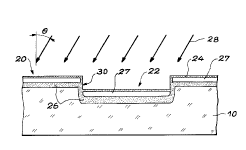
Fig. 3 illustrates the formation of a buried silicon oxide layer 26.
In order to form said layer, oxygen ions are implanted in the sili-
con wafer 10 through its surface. It should be noted in this con-
nection that the silicon oxide layer 24 previously formed on the
substrate surface makes it possible to dechannel, i.e. accurately
control the projecting beam of implanted oxygen ions so as to
obtain implanted zones with homogeneous oxygen concentrations.
After implantation, annealing is carried out in order to obtain and
render coherent the layer 26. The layer 26 then defines in the
silicon wafer 10 a surface silicon layer 27, which it electrically
insulates from a solid silicon part of the wafer.
The energy and dose of the implanted ions are chosen so as to form
the layer 26 at a given depth in the first and second regions 20,
22. For example, the layer 26 is buried at a depth between 10 and
200 nm. For producing a buried silicon oxide layer, reference can
be made to document (2), whose reference is indicated at the end of
B 12382.3/EW
22~264
-- 10 --
the description.
The layer 26 follows the level difference pattern of the substrate
surface. Thus, it is buried at an equal depth beneath the sub-
strate surface in the first and second regions.
Arrows 28 in fig. 3 give an oxygen ion implantation beam orienta-
tion. It forms an angle ~ with respect to the perpendicular to the
substrate plane. Thus, ions are also implanted in the transition
flank 30 between the regions 20 and 22, at least on one side of
the second region 22. In order to avoid ion deficit by shading of
the planes, the wafers are rotated so as to implant the same dose
on all the flanks. The ion dose implanted in the transition flank
30 is equal to D.cosa, in which D is the implantation dose in the
first and second regions.
The implantation angle is chosen sufficiently small, i.e. the
oxidation profile is made sufficiently steep to ensure that the
layer 26 buried in the regions 20, 22 is substantially level with
the surface of the transition flank 30. It is considered that the
layer 26 is substantially level with the surface, when it is pres-
ent at the surface or when it is close to the surface, i.e. buried
at a very small depth.
In the case where the buried layer 26 is not present at the surface
of the flank 30, but at a limited depth beneath the surface, it is
also possible to carry out an oxidation in order to thicken the
surface oxide layer 24 until the latter reaches the buried layer in
the region of the transition flank 30.
A following stage consists of carrying out a partial deoxidation
making it possible to completely eliminate the oxide layer 24 at
the substrate surface and eliminate the oxide of the layers 24 and
26 on the transition flank 30. The silicon layer and the silicon
B 12382.3/EW
~25~1264
of the wafer 10 on the flank 30 are consequently exposed.
The structure shown in fig. 4 is obtained by forming on the exposed
silicon a monocrystalline silicon layer 32. This layer is formed
by epitaxy, preferably at a temperature between 850 and 1300~C, e.g.
at 1100~C.
The epitaxy is controlled from the surface layer 27 in the first
and second regions 20, 22 and from the silicon on the flank 30.
Advantageously, the epitaxying of the monocrystalline layer 32 can
be preceded by annealing in order to eliminate any residual contam-
ination and reduce to the minimum the defects in the silicon layer
27.
A following stage consists of smoothing and levelling the silicon
layer stopping at the layer 26 of the first region 20. This takes
place e.g. by a mechanochemical polishing. The structure shown in
fig. 5 is obtained.
The "buried" layer 26 of the first region 20 is exposed and there-
after appears at the surface of the substrate. In the second
region 22, the silicon oxide layer 26 remains covered by the sili-
con layer 27 and by the monocrystalline silicon layer 32, whose
thickness has been reduced during levelling. The substrate surface
in the first and second regions is in the same plane following this
stage.
A following stage consists of an oxidation of the substrate surface,
as shown in fig. 6. By forming a new silicon oxide layer 34, this
stage makes it possible to thicken the silicon oxide layer 26 in
the first region 30 and thin the silicon layer 32 in the second
region 22.
B 12382.3/EW
220026~
- 12 -
An implantation of doping impurities leading to a doping of the
same conductivity type as the substrate wafer 10 is carried out
through the layer 34. In the present case they are boron impuri-
ties, leading to a p type doping.
Implantation, materialized by the arrows in fig. 7, makes it pos-
sible to form a p type doped zone 36 extending beneath the silicon
oxide layer 26 in the first region 20 and above the layer 26 in the
second region 22. In the second region 22, the doped zone corr-
esponds to the layer 27 and at least part of the layer 32.
The doped zone 36 passing into the region of the transition flank
30 between the regions 20 and 22 makes it possible to improve elec-
trical contacting between the part of the second region above the
silicon oxide layer 26 and referred to hereinafter as the "active"
region 38 and the solid part of the silicon wafer 10. Zone 36 also
has a latch-up-preventing function in the active region 38, where
the transistors are subsequently formed.
Partial deoxidation is followed by boron implantation. It permits
the exposure of the active part 38, whose layer 32 has been thinned,
whilst preserving an also thinned part of the silicon oxide layer
26 in the first region. This gives the structure shown in fig. 8.
When the formation of the silicon oxide layer is performed at a
relatively high temperature of approximately 1050~C, at the end of
deoxidation a rounded edge is obtained between the active part 38
and the silicon oxide layer 26. This rounded edge is given the
reference numeral 40.
The substrate finally obtained has a series of recesses with a
SOI structure. They are second regions mutually insulated at the
surface by the silicon oxide layer of the first region.
B 12382.3/EW
2~0~64
- 13 -
One or more contact pieces formed through the flanks of the rec-
esses according to the process described hereinbefore, make it pos-
sible to remove the charges (holes) accumulated in the active
regions towards the solid part of the substrate and prevent in this
way the kink effect. The contact pieces are designated 39 in fig.
8.
Figs. 9 and 10 illustrate a use of the substrate prepared in the
aforementioned manner in order to produce a field effect transis-
tor. The production stages for the transistor are briefly des-
cribed below.
Fig. 9 shows the formation, particularly at the surface of the
active region, of a gate oxide layer 50 (SiO2) and the deposition
of a gate material layer 52, e.g. polycrystalline silicon. The
layer 52 is then shaped by the formation of a not shown mask and
by selective etching, in order to obtain a gate 54 as shown in
fig. 10.
Source 56 and drain 58 regions are produced in the active region
by implantation using the gate 54 as a mask.
The regions 56 and 58 are preferably produced by a double implant-
ation, e.g. with ions leading to a conductivity of the opposite
type to that of the solid silicon wafer of the substrate, i.e.
opposite to that of the active region.
A first implantation with a low dose is followed by the formation
of lateral spacers 60 on the gate 54 and by a second implantation
at a higher dose.
In the illustrated case, an implantation of ions leading to a n
type conductivity permits the formation of a n channel transistor.
B 12382.3/EW
2~ 64
The thus produced transistor or circuits do not have a floating
potential parasitic base. Thus, they are freed from the kink
effect and consequently the transistor is biased with voltages
higher than those generally accepted for MOS devices on SOI sub-
strates. This property also leads to the advantage of permitting
an increase in the performance characteristics of the thus produced
transistors.
CITED DOCUMENTS
(1) "Analysis of Kink Characteristics in Silicon-on-Insulator
MOSFET's Using Two-carrier Modeling" by KOICHI KATO et al., IEEE
Transaction on electron devices, vol. E.D. 32, No. 2, February 1985,
pp 458-462
(2) Microstructures of silicon implanted with high dose oxygen
ions by C. Jaussaud et al. Appl. Phys. Lett. 46 (11), 1 June 1985,
pp 1064-1066.
B 12382.3/EW