Note: Descriptions are shown in the official language in which they were submitted.
CA 02200300 2000-08-24
Description
EFFICIENT OPTICAL WAVELENGTH
MULTIPLEXER/DE-MULTIPLEXER
Technical Field
This invention relates to wavelength coupling
and more particularly to efficient wavelength
coupling of a plurality of wavelengths onto an
optical fiber.
Background Art
It is known in the art of high speed optical
communication systems that more that one wavelength
may be used to carry information. In particular,
each optical wavelength may be a carrier for digital
or analog communication signals. Also, an optical
switch may be used to discriminate on a wavelength
basis as to which wavelengths get routed to which
outputs) of the switch.
One prior art technique to couple a plurality of
wavelengths, e.g. 8, onto a signal fiber employs an
arrangement of 2x2 couplers as shown in Fig. 1. In
particular, two different wavelengths are fed into
each 2x2 coupler in an input stage. A single output
from each of the 2x2 couplers is fed to a second
stage, where a single output from each pair of
couplers is combined by another 2x2 coupler. A
- 1 -
WO 96/09703 ~ 2 ~ Q 3 p ~ PCT/US95112231
single output from each of the 2x2 couplers in the
second stage is then fed to a third stage where each
pair of outputs from the second stage is combined by
.
another 2x2 coupler in the third stage.
The prior art arrangement shown in Fig. 1
couples eight wavelengths on eight separate fibers
at the input stage to a single fiber at the output
of the output stage. However, because there are
three stages of coupling which occurs, and each
stage incurs a 3 dB loss in the signal coupled, the
total loss for a eight wavelength to one fiber
coupling would be 87.5% loss (or 9 dB).
Thus, it would be desirable to obtain a device
for efficient low loss multiplexing of a plurality
of wavelengths onto a single optical fiber.
Disclosure of Invention
Objects of the invention include provision of
an efficient multiplexing configuration for coupling
a plurality of wavelengths on to a single optical
2 0 fiber .
According to a first aspect of the present
invention an optical wavelength multiplexes includes
an optical coupler, having an input port, two bi-
directional ports, and an output port, which couples
a predetermined amount of a first input signal at
the input port to the two bi-directional ports as
coupled input light; a pair of reflective elements,
each in the path of light exiting from one of the
two bi-directional ports, and each having a
predetermined reflectivity profile; the reflective
elements each reflecting a predetermined wavelength-
band of the coupled input light incident thereon
back into a corresponding one of the two bi-
directional ports as reflected input light; a
predetermined amount of each of the reflected input
light re-entering the corresponding one of the two
- 2 -
WO 96/09703 PCT/US95/12231
22 00 goo
bi-directional ports and being coupled by the
coupler to the output port and the input port; the
reflective elements, the coupler, anc't optical path
lengths traveled by the coupled input: light and the
reflected input light having a cumulative phase
shift such that light which is coupled to the input
port destructively interferes at the input port and
the light which is coupled to the output port
constructively interferes at the output port,
thereby providing substantially all of the first
input light to the output port; one of the pair of
reflective elements having a second input signal
incident thereon and passing a predetermined
wavelength-band of the second input signal which
enters a corresponding one of the twa bi-directional
ports; a predetermined amount of the second input
signal entering the corresponding one: of the two bi-
directional ports being coupled by th.e coupler to
the output port; and thereby coupling' a
predetermined wavelength-band.of the first input
signal and a predetermined wavelength.-band of the
second input signal to the output port.
According further to the first aspect of the
present invention, the other of the pair of
reflective elements having a third input signal
incident thereon and passing a predetermined
wavelength-band of the third input signal which
enters a corresponding one of the twa bi-directional
ports; a predetermined amount of the third input
signal entering the corresponding one of the two bi-
directional ports being coupled by the coupler to
the output port; and thereby coupling a
predetermined wavelength-band of the first input
signal, the second input signal and the third input
signal to the output port.
- 3 -
WO 96/09703 ~ ~ ~ ~ ~ ~ PCT/US95/12231
Still further according to the first aspect of
the present invention, the pair of reflective
elements have matching reflectivity profiles.
According to a second aspect of the present
invention, an optical wavelength de-multiplexes
includes an optical coupler, having an input port,
two bi-directional ports, and an output port, which
couples a predetermined amount of a first input
signal at the input port to the two bi-directional
ports as coupled input light; a pair of reflective
elements, each in the path of light exiting from one
of the two bi-directional ports, and each having a
predetermined reflectivity profile; the reflective
elements each reflecting a predetermined wavelength-
band of the coupled input light incident thereon
back into a corresponding one of the two bi-
directional ports as reflected input light and at
least one of the pair of reflective elements passing
a predetermined wavelength band of the coupled input
light to an associated output waveguide; a
predetermined amount of each of the reflected input
light re-entering the corresponding one of the two
bi-directional ports being coupled by the coupler to
the output port and the input port; the reflective
elements, the coupler, and optical path lengths
traveled by the coupled input light and the
reflected input light having a cumulative phase
shift such that light which is coupled to the input
port destructively interferes at the input port and
the light which is coupled to the output port
constructively interferes at the output port,
thereby providing substantially all of the first
input light to the output port; and thereby coupling
a predetermined wavelength-band of the first input
signal to the output waveguide.
- 4 -
WO 96/09703 PCT/US95/12231
22 ~1~ 300
According further to the second aspect of the
present invention, the pair of reflective elements
have matching reflectivity profiles.
The invention represents a significant
improvement over the prior art by providing an
efficient multiplexing configuration that simply and
inexpensively couples a plurality of individual
wavelengths onto a single optical fiber.
Alternatively, the invention may also be used as a
demultiplexer to separate out individual wavelengths
from one input having a plurality of wavelengths to
a plurality of separate outputs.
The foregoing and other objects, features and
advantages of the present invention will become more
apparent in light of the following deaailed
description of exemplary embodiments thereof as
illustrated in the accompanying drawings.
Brief Description of Drawings
Fig. 1 is a prior art wavelength. multiplexing
arrangement.
Fig. 2 is a prior art bandpass filter having a
Michelson interferometer arrangement.
Fig. 3 is a schematic block diagram of a
multiplexing configuration for coupling a plurality
of wavelengths onto a single optical fiber, in
accordance with the present invention.
Fig. 4 is a graph of reflectivity against
wavelength for a bandpass filter function created by
one or more Bragg gratings, in accordance with the
present invention.
Fig. 5 is a schematic block diagram of an'
alternative embodiment for a multiplexing
configuration for coupling a plurality of
wavelengths onto a single optical fiber using less
couplers, in accordance with the present invention.
- 5 -
WO 96/09703 PCT/US95/12231
22 00 300
Fig. 6 is a schematic block diagram of an
alternative application of the present invention as
a demultiplexer, in accordance with the present
invention.
V
Best Mode for Carrying out the Invention
Referring to Fig. 2, a prior art Michelson
interferometer-based bandpass filter arrangement of
the prior art comprises a 2x2 optical coupler 10,
e.g., a 3 dB or 50% or 50/50 optical coupler, which
receives an input signal 12 along an optical fiber
14 which is fed to a port 16 of the coupler 10. A
predetermined portion of the input light 12, e.g.,
50%, exits a port 18 of the coupler 10 as indicated
by a line 20 along a fiber 22. The remaining
portion of the light 12 is coupled to a port 24 of
the optical coupler 10 as indicated by a line 26
along a fiber 28.
The light 20 travels along the fiber 22 and is
incident on a Bragg grating 30 which reflects a
narrow wavelength band of light centered at a
reflection wavelength fig, as indicated by a line 32
and passes all remaining wavelengths, as indicated
by a line 34.
The light 26 that exits the coupler 10 along
the fiber 28 is incident on a grating 38, identical
to (or matching) the grating 30, having a central
reflection wavelength centered at the wavelength
A reflectivity profile (or filter function) of the
gratings 30,38 is shown by the curve 39. The light
reflected at the wavelength ~g by the grating 38 is
indicated by a line 40 and all remaining wavelengths
are passed by the grating 38 as indicated by a line
42. The light 32 re-enters the coupler 10 at the '
port 18 and the reflected light 40 re-enters the
coupler 10 at the port 24. This is similar to the
basic principle of a Michelson interferometer that
- 6 -
WO 96/09703 PCT/US95/12231
2 2 00 300
well known in the optical art. The signal 12 which
enters the port 16 of the coupler 10 incurs a phase
shift of ~r/2 upon coupling to the opposite leg and
exiting the output port 24 along the fiber 28. Upon
reflecting off the grating 38, the signal 26
experiences another n/2 due the reflection from the
grating 38. As a consequence, there is a net total
phase shift of 180 or ~r from the input signal 12 to
the reflected signal 40. Similarly, the light 12
entering the coupler 16 is also coupled to the
output port 18 on the fiber 22 as the: signal 20
without any phase shift. The signal 20 is reflected
off the grating 30 as the signal 32 which
experiences a ~r/2 or 90 phase shift. The signal 32
re-enters the coupler 10 at the port 18 and the
portion which crosses-over to the port 50
experiences an additional ~r/2 phase shift due to the
crossover. Thus, the signal 54 exiting the coupler
50 comprises the wavelength ~g of the input signal
12 which has been split 50/50 and then recombined
completely in-phase so ws to constructively
interfere at the output port 50 of the coupler 10,
thereby providing substantially the input signal 12
at the wavelength ~g at the output fiber 152.
Similarly, there is destructive interference at the
port 16 thereby preventing any light 56 from exiting
the coupler 10 along the fiber 14. In particular,
the reflected light 40 from the grating 38 which re-
enters the coupler 10 at the port 24 is coupled over
to the port 16 and incurs an additional ~t/2 phase
shift, thereby having incurred a total of 270 (or
3~r/2) phase shift. However, the reflected light 32
from the grating 30 which re-enters the port 18 has
' experienced a ~r/2 or 90 phase shift and is coupled
to the port 16 without experiencing any additional
phase shift. Thus, the returning signal 32 has
incurred a total of 90 phase shift and the
WO 96/09703 2 2 ~ 0 3 0 p P~~S95/12231
returning signal 40 at the port 16 has incurred a
total of 270° phase shift, thereby having a 180°
phase shift between the signals and thus
destructively interfering at the input port 16.
Therefore, no light 56 from exits the input port 16
along the fiber 14. Such a device is described in
the publication W. W. Morey, "Tunable Narrow-Line
Bandpass Filter Using Fiber Gratings," Technical
Digest, Optical Fiber Communication Conference, San
Diego, California, February 18-22, 1991, which is
incorporated herein by reference.
Because the amount of phase shift of each
signal is important for proper operation, the length
of the optical path from the port 18 to the grating
30 must be the same as, or an integral i number of
wavelengths of, the optical path length from the
port 24 to the grating 38. Also, it should be
understood that these optical path lengths may cause
the total phase shift for the signals to be
different than the example discussed hereinbefore;
however, it is only required that the phases cancel
at the input port 16 and add at the output port 50,
to provide no reflection of the input wavelengths to
the couplers. If the phases do not perfectly
cancel, some amount of reflection will be seen. The
amount of allowable reflection is determined by the
application. Consequently, thermal effects should
also be kept constant or matched for both path
lengths to avoid changes in the amount of light
reflected. Also, it should be understood that the
amount of phase shift may be other than 90 degrees
after being reflected from the grating for '
wavelengths of the incident light at other than the
reflection wavelength of the grating. Referring now
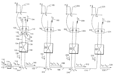
to Fig. 3, a first embodiment of the present
invention accepts an input signal 110 which
propagates along an optical fiber 112 to an optical
_ g _
WO 96/09703 PCT/US95/12231
22 00 300
isolator 114. The output of the iso7.ator 114
provides an optical signal 116 on an optical fiber
118 to a port 120 of a 2x2 optical coupler 122,
e.g., a 3 dB or 50/50 or 50% optical coupler. A
predetermined portion, e.g., 50% of t;he input signal
116 is coupled to an output port 124 of the coupler
122 as indicated by a line 126, along a fiber 128.
The light 126 is incident on the fiber Bragg grating
130. The grating 130 has a reflection profile, as
indicated by a curve 131, of a narrow bandpass or
filter having central part of the bandpass region at
the wavelength ~1 which is the same as the
reflection wavelength of the grating 130. Thus, the
grating 130 passes a narrow wavelength band of light
~I as indicated by a line 132 and reflects the
remaining wavelengths as indicated by a line 134.
Symmetrically, the remaining portion of the
light 116 exits the coupler 122 from a port 136 on a
fiber 138 as indicated by a line 140. Line 140 is
incident on a grating 142 which is identically
matched in reflectivity profile to that of the
grating 130. The grating 142 passes a narrow
wavelength band of light centered at the wavelength
~1 as indicated by a line 144 and pas:aes the
remaining wavelengths as indicated by a line 146.
The reflected light 132,144 from the matched
gratings 130,142 re-enter the coupler 122 at the
ports 124,136, respectively, and constructively
interfere within the coupler 122 as discussed
hereinbefore with respect to Fig. 2 such that all
the reflected light at the wavelength ~o exits a
port 150 of the coupler 122. Because light both
exits and re-enters the ports 124,136, they may be
referred to as "bi-directional" ports herein.
Additionally, another input signal 154 travels
along the fiber 138 and is incident on the fiber
grating 142, such signal 154 having a wavelength ~1
- 9 -
WO 96109703 PCT/US95112231
2 2 00 300
which passes through the grating 142 and enters the
coupler 120 at the port 136. As indicated by a line
156, a predetermined portion, e.g., 50%, of the
light 56 is coupled to the port 120 along the fiber
118 as indicated by a line 158. Similarly, the
remaining portion, e.g., 50%, of the light 156 is
coupled to the output port 150 along the fiber 152.
The wavelengths ~o and ~1 which exit the coupler 122
at the port 150 along the fiber 152 are collectively
indicated by a line 160. The light 158 travels
along the fiber 118 and enters the isolator 114
which prevents the light 158 from exiting the input
port along the line 112.
Therefore, the wavelength ~i has been coupled
onto the fiber 52 along with the wavelength
Also, the wavelength ~1 on the fiber 152 experiences
a 3 dB or 50% attenuation. However, the input
signal 110 of ~o experiences minimum attenuation.
The fiber 152 is fed to a similar configuration
as that discussed hereinbefore with the coupler 122
comprising a 2x2 coupler 180 and a pair of matched
gratings 182,184 each of which has a bandpass
reflectivity profile as shown by a curve 185 such
that the wavelength ~2 is passed and all other
wavelengths are reflected. Consequently, the
wavelengths ~0,~1 on the input line 160 to the
coupler 180 are coupled directly to the output along
a fiber 186 as indicated by a line 188.
Additionally, an input signal 190 comprising a
wavelength ~Z is incident on the grating 184 and
exits the coupler along the fiber 152 as indicated
by a line 192 and a line 188. The light 190 is
coupled 50/50 along each of the fibers 152,186,
respectively. Thus, the wavelengths ~o,~i,~z
propagate along the fiber 186.
The fiber 186 is fed again to a similar
arrangement comprising a 2x2 coupler 200 and a pair
- 10 -
WO 96/09703 PCT/US95/12231
r 22 00 300
of matched gratings 202,204 each having a bandpass
reflectivity characteristic centered at ~3, as shown ,
by a curve 205. Additionally, an input signal 206
is incident on the grating 204 which passes the
wavelength ~3 and enters the coupler 200, and a
portion thereof, e.g., 50%, exits thsa coupler,200 as
indicated by a line 208, and the remaining portion
exits the coupler 200 on a fiber 210,, as indicated
by a line 212. The wavelengths Ao, A1, ~z are
coupled in their entirely to the fibs:r 210, thereby
adding in the wavelength ~3 to the prior chain of
~o. Vii. ~z. all along the fiber 210.
The fiber 210 is fed to a similar arrangement
as the prior configurations comprising a 2x2 coupler
220 and a pair of matched gratings 222,224 which
both have a bandpass reflectivity profile centered
at the wavelength ~4 as indicated by a curve 225 and
which provide the Michelson interferometer effect
discussed hereinbefore. Thus, the entire signal 212
comprising the wavelengths ~o, ~1, ~z, ~3 is coupled over
to an output fiber 226, as indicated by a line 228.
Additionally, an input signal 230 having a
wavelength ~4 is incident on the grating 224 which
passes the wavelength ~4. The signal 230 then
passes to the coupler 220 which coup7.es a
predetermined portion, e.g., 50%, of the signal 230
onto the fiber 226, which is combined with the other
wavelengths to provide an output signal 228 on the
fiber 22 6 having the wavelengths Ao, ~z, a2. ~3. ~a ~ The
rest of the signal 230 is coupled to the fiber 210
as indicated by the line 232. Also, the reflected
signals 158,192,208,232 from the couplers
122,180,200,220 are successively pas~~ed backwards
along the chain as indicated by the lines
249,242,244 which ultimately pass to the isolator
114 which does not allow such signals to exit the
input fiber 112 and disrupt up-stream sources, and
- 11 -
CA 02200300 2000-08-24
does not reflect such signals back into the coupler 122.
It should be understood that this progression may
continue for any number of wavelengths and the maximum
degradation or attenuation which occurs on any of the
input signals is an initial 3 dB attenuation only (plus
any additional small loss due to coupler loss or due to
not having gratings with 100 reflection), independent of
the number of wavelengths to be coupled onto the output
fiber.
Referring to Fig. 4, to make the narrow bandpass
reflectivity profile shown by the curves 131, 185, 205,
225 of Fig. 3, the grating may be made by two broad
reflectivity band gratings 100, 102 placed side by side
having a predetermined wavelength spacing ~,S therebetween.
The wavelength spacing ~,5 is the bandpass region, with the
center of that region ~,$ being the center of the bandpass
profile as indicated in Fig. 4. The broadband
reflectivity profiles 100, 102 may be created as is known
by a chirped or aperiodic refractive index variation
distribution along the core of the fiber such as is
discussed in U.S. Patent Number 5,388,173 entitled
"Method and Apparatus for Forming Aperiodic Gratings and
Optical Fibers".
To date, broadband (e. g., 15 nm) gratings have been
fabricated in highly photosensitive hydrogen load fibers.
Broader chirped gratings can be fabricated
interferometrically by placing appropriate radii of
curvatures on the interfering beams. Another technique
is to use known phase masks, with the grating chirp and
transmission notch profiles encoded, which exposes the
proper grating profile into the fibers in a reliable and
3
repeatable way.
- 12 -
WO 96/09703 PCT/US95/12231
~ ~22 00 300
Referring again to Fig. 3, the coupler
122,180,200,220 may be a fused tapered coupler which
is currently commercially available in
photosensitive fibers such as a Corning SMF 28.
Since this technology is well established it is
possible to procure these tapered couplers in more
highly photosensitive specialty fiber's. In
addition, the use of techniques such as hydrogen
loading to increase fiber photosensitivity is also
possible. In order to maximize efficiency, the
grating's should be highly reflective and
sufficiently broadband to cover the required
bandwidth of the wavelength division multiplexed
system. Maintenance of relatively short
interferometer arms that the gratings. are located on
help to minimize interferometer sensitivity due to
environmental effects. Also, the gratings may be
written before the fused tapered coupler is
packaged, thereby providing very short distance
between the gratings the point where the signals are
coupled. Also, as discussed hereinbefore and in the
aforementioned OFC proceedings paper, the optical
path lengths between each of the matched gratings
and its respective coupler must be the same or
differ by an integral number of wavelengths for
constructive interference to occur.
Referring now to Fig. 5, an alternative
embodiment of the present invention uses the same
basic coupler/grating arrangement as in Fig. 3
except that input signals are provided into both
arms of the coupler. In this configuration, the
gratings associated with a given coupler each have a
different bandpass wavelength, as indicated by the
curves 300-314. This allows the coupling of two
wavelengths onto the output fiber of a given coupler
instead of coupling only one wavelength. This
configuration is more efficient than the embodiment
- 13 -
WO 96109703 PCT/US95/12231
22 00 300
of Fig. 3 by requiring only one-half the number
couplers to couple the same number of wavelengths.
It should be understood that the phase shift and
reflectivity should be the same for gratings at the
wavelengths being reflected back into the couplers
(i.e., at other than the bandpass wavelengths) to
ensure proper phase interaction (constructive and
destructive interference) for the Michelson
interferometer portion of the configuration,
discussed hereinbefore.
Alternatively, for ease of fabrication with the
embodiment of Fig. 5 and to maximize matching of
gratings, the two gratings associated with a given
coupler may pass both wavelengths (e.g., ~1 and ~
for the coupler 122, Fig. 5), thus placing two
wavelength bandpass regions on each grating, as
indicated by the curve 320. In that case, the
gratings for a given coupler would have identical
filter functions, thereby allowing the gratings to
be made simultaneously and ensuring that the phase
shift of each grating is the same at non-bandpass
wavelengths, to ensure proper phase interaction
(constructive and destructive interference) for the
Michelson interferometer portion of the
configuration, discussed hereinbefore.
Referring now to Fig. 6, alternatively, the
invention may be used as a demultiplexer. In that
case, the input signal 110 is a broad wavelength-
band signal comprising a plurality of wavelengths,
e.g., ~1 - ~8. If the gratings are configured with
the reflectivity profiles shown by the curves 300-
314 of Fig. 5, each leg of the couplers that have a '
grating associated therewith allows the passband
wavelength to pass as an output signal, as indicated -
by the solid lines 400-414. In that case, some of
each input wavelength will exit the ports 120,150.
Alternatively, if the gratings are matched and
- 14 -
WO 96!09703 PCT/US95/12231
~ 2 00 300
configured with the reflectivity profiles shown by
the curves 131,185, 205,225 of Fig. 3, both legs of
each coupler having gratings associated therewith
pass the same passband wavelength so only one leg
need be used as an output signal, as indicated by
the dashed lines 420-426. Also, in 'that case, the
isolator 114 is not needed.
Thus, when used in this application, the
invention takes an input signal having a plurality
of wavelengths and demultiplexes the wavelengths
onto a plurality individual output lines, thereby
providing an efficient all-fiber wavelength de-
multiplexer. Also, the isolator 114 at the input to
the device may not be needed if the lKichelson
interferometer coupler/grating arrangement discussed
hereinbefore provides no reflected wavelengths out
of the input port 120 of the coupler 120, as would
typically be the case.
- 15 -