Note: Descriptions are shown in the official language in which they were submitted.
-i
22 00 305
VERTICAL GEOMETRY LIGHT EMITTING DIODE WITH GROUP III
NITRIDE ACTIVE LAYER AND EXTENDED LIFETIME
Field Of The Invention
This invention relates to optoelectronic
devices and more particularly to light emitting diodes
formed from Group III nitrides (i.e., Group III of the
Periodic Table of the Elements) that will produce
output in the blue to ultraviolet portions of the
electromagnetic spectrum.
Background Of The Invention
Light emitting diodes ("LEDs") are p-n
junction devices that have been found to be useful in
various roles as the field of optoelectronics has grown
and expanded over the years. Devices that emit in the
visible portion of the electromagnetic spectrum have
been used as simple status indicators, dynamic power
level bar graphs, and alphanumeric displays in many
applications, such as audio systems, automobiles,
household electronics, and computer systems, among many
others. Infrared devices have been used in conjunction
with spectrally matched phototransistors in
optoisolators, hand-held remote controllers, and
interruptive, reflective, and fiber-optic sensing
applications.
An LED operates based on the recombination of
electrons and holes in a semiconductor. When an
electron carrier in the conduction band combines with a
22 00 30 5
-2-
hole in the valence band, it loses energy equal to the
bandgap in the form of an emitted photon; i.e., light.
The number of recombination events under equilibrium
conditions is insufficient for practical applications
but can be enhanced by increasing the minority carrier
density.
In an LED, the minority carrier density is
conventionally increased by forward biasing the diode.
The injected minority carriers radiatively recombine
with the majority carriers within a few diffusion
lengths of the junction edge. Eaclz recombination event
produces electromagnetic radiation, i.e, a photon.
Because the energy loss is related to the bandgap of
the semiconductor material, the bandgap characteristics
of the LED material has been recognized as being
important.
o As with other electronic devices, however,
there exists both the desire and the need for more
efficient LEDs, and in particular, LEDs that will
operate at higher intensity while using less power.
Higher intensity LEDs, for example, are particularly
useful for displays or status indicators in various
high ambient environments. There also is a relation
between intensity output of the LED and the power
required to drive the LED. Low power LEDs, for
example, are particularly useful in various portable
electronic equipment applications. An example of an
attempt to meet this need for higher intensity, lower
power, and more efficient LEDs may be seen with the
development of the AlGaAs LED technology for LEDs. in
the red portions of the visible spectrum. A similar
continual need has been felt for LEDs that will emit in
the blue and ultraviolet regions of the visible
spectrum. For example, because blue is a primary
color, its presence is either desired or even necessary
to produce full color displays or pure white light.
22 00 30 5
-3-
The common assignee of the present patent
application was the first in this field to successfully
develop commercially viable LEDs available in large
quantities and that emitted light in the blue color
spectrum. These LEDs were formed in silicon carbide, a
wide bandgap semiconductor material. Examples of such
blue LEDs are described in U.S. Patent Nos. 4,918,497
and 5,027,168 to Edmond each titled "Blue Light
Emitting Diode Formed In Silicon Carbide."
Other examples of such a blue LED are
described in U.S. Patent No. 5,306,662 to Nakamura et
al. titled "Method Of Manufacturing P-Type Compound
Semiconductor" and U.S. Patent No. 5,290,393 to
Nakamura titled "Crystal Growth Method For Gallium
Nitride-Based Compound Semiconductor." U.S. Patent No.
5,273,933 to Hatano et al. titled "Vapor Phase Growth
Method Of Forming Film In Process Of Manufacturing
Semiconductor Device" also describes LEDs formed of
GaInAlN on SiC substrates and Zinc Selenide (ZnSe) on
gallium arsenide (GaAs) substrates.
As known to those familiar with photonic
devices such as LEDs, the frequency of electromagnetic
radiation (i.e., the photons) that can be produced by a
given semiconductor material are a function of the
material's bandgap. Smaller bandgaps produce lower
energy, longer wavelength photons, while wider bandgap
materials are required to produce higher energy,
shorter wavelength photons. For example, one
semiconductor commonly used for lasers is indium
gallium aluminum phosphide (InGaAIP). Because of this
material's bandgap (actually a range of bandgaps
depending upon the mole or atomic fraction of each
element present), the light that InGaAlP can produce is
limited to the red portion of the visible spectrum,
i.e., about 600 to 700 nanometers (nm).
working backwards, in order to produce
photons that have wavelengths in the blue or
22 0~ 305
-4-
ultraviolet portions of the spectrum, semiconductor
materials are required that have relatively large
bandgaps. Typical candidate materials include silicon
carbide (SiC) and gallium nitride (GaN).
Shorter wavelength LEDs offer a number of
advantages in addition to color. In particular, when
used in optical storage and memory devices (e. g., "CD-
ROM" or "optical disks"), their shorter wavelengths
enable such storage devices to hold proportionally more
information. For example, an optical device storing
information using blue light can hold approximately 32
times as much information as one using red light, in
the same space.
Gallium nitride, however, is an attractive
LED candidate material for blue and UV frequencies
because of its relatively high bandgap (3.36 eV at room
temperature) and because it is a direct bandgap
material rather than an indirect bandgap material. As
known to those familiar with semiconductor
characteristics, a direct bandgap material is one in
which an electron's transition from the valence band to
the conduction band does not require a change in
crystal momentum for the electron. In indirect
semiconductors, the alternative situation exists; i.e.,
a change of crystal momentum is required for an
electron's transition between the valence and
conduction bands. Silicon and silicon carbide are
examples of such indirect semiconductors.
Generally speaking, an LED formed in a direct
bandgap material will perform more efficiently than one
formed in an indirect bandgap material because the
photon from the direct transition retains more energy
than one from an indirect transition.
Gallium nitride suffers f-_rom a different
disadvantage, however: the failure to date of any
workable technique for producing bulk single crystals
of gallium nitride which could form appropriate
i
22 00 305
-5-
substrates for gallium, nitride photonic devices. As is
known to those familiar with semiconductor devices,
they all require some sort of structural substrate.
Typically, a substrate formed of the same materials as
the active region of a device offers significant
advantages, particularly in crystal growth and
matching. Because gallium nitride has yet to be formed
in such bulk crystals, however, gallium nitride
photonic devices must be formed in epitaxial layers on
different--i.e., other than GaN--substrates.
Using different substrates, however, causes
an additional set of problems, mostly in the area of
crystal lattice matching. In almost all cases,
different materials have different crystal lattice
parameters. As a result, when a gallium nitride
epitaxial layer is grown on a different substrate, some
crystal mismatch will occur, and the resulting
epitaxial layer is referred to as being "strained" by
this mismatch. Such mismatches, arid the strain they
produce, carry with them the potential for crystal
defects which in turn affect the electronic
characteristics of the crystals and the junctions, and
thus correspondingly tend to degrade or even prevent
the performance of the photonic device. Such defects
are even more problematic in higher power structures.
To date, the most common substrate for
gallium nitride devices--and the only substrate
utilized in GaN LED's--has been sapphire; i.e.,
aluminum oxide (A1203). Sapphire is optically
transparent in the visible and UV ranges, but is
unfortunately insulating rather than conductive, and
carries a lattice mismatch with gallium nitride of
about 16%. In the absence of a conductive substrate,
"vertical" devices (those with contacts on opposite
sides) cannot be formed, thus complicating the
manufacture and use of the devices.
2~ 00 305
-6-
As a particular disadvantage,horizontal
structures (those with contacts on the same side of the
device), such as those required when gallium nitride is
formed on sapphire, also produce a. horizontal flow of
current and therefore the current density through the
layer is substantially increased. This horizontal
current flow puts an additional strain on the already-
strained (i.e., the 16% lattice mismatch) GaN-sapphire
structure and accelerates the degradation of the
junction and the device as a whole.
Gallium nitride also carries a lattice
mismatch of about 2.4% with aluminum nitride (A1N) and
a 3.5% mismatch with silicon carbide. Silicon Carbide
has a somewhat lesser mismatch (only about 10) with
aluminum nitride.
Group III ternary and quaternary nitrides
(e.g., InGaN, InGaAIN, etc.) have also been shown to
have relatively wide bandgaps and thus also offer the
potential for blue and ultraviolet semiconductor
lasers. Most of these compounds, however, present the
same difficulty as gallium nitride: the lack of an
identical single crystal substrate. Thus, each must be
used in the form of epitaxial layers grown on different
substrates. Thus, they present the same potential for
crystal defects and their associated electronic
problems:
Obiect And Summary Of The Invention
Therefore, it is an object of the present
invention to provide a light emitting diode that can
emit in the blue and ultraviolet portions of the
electromagnetic spectrum, that can be built in the
vertical geometry that is most advantageous for such
devices, that has excellent brightness and efficiency
and that can exhibit better physical and electronic
longevity and performance than can previously available
diodes.
CA 02200305 1999-11-12
The invention meets this object with a light
emitting diode that emits in the blue portion of the
visible spectrum and that is characterized by an extended
lifetime because of its advantageous materials and
structure. The light emitting diode comprises a
conductive silicon carbide substrate; an ohmic contact to
the silicon carbide substrate; a conductive buffer layer
on the substrate and selected from the group consisting
of gallium nitride, aluminum nitride, indium nitride,
ternary Group III nitrides having the formula AxBl_XN,
where A and B are Group III elements and where x is zero,
one, or a fracaion between zero and one, quaternary Group
III nitrides raving the formula AXByCl_x_yN where A, B, and
C are Group III elements; x and y, are zero, one, or a
fraction between zero and one, and 1 is greater than (x +
y), and alloy: of silicon carbide with such ternary and
quaternary Group III nitrides; and a double
heterostructure including a p-n junction on the buffer
layer in whicr, the active and heterostructure layers are
selected from the group consisting of binary Group III
nitrides, ternary Group III nitrides, quaternary Group
III nitrides, and alloys of silicon carbide with such
nitrides.
The foregoing and other objects, advantages and
features of th.e invention, and the manner in which the
same are accomplished, will become more readily apparent
upon consideration of the following detailed description
of the invention taken in conjunction with the
accompanying drawings, which illustrate preferred and
exemplary embodiments, and wherein:
In accordance with an aspect of the invention
there is provided a light emitting diode that emits in
the blue portion of the visible spectrum and that is
characterized by an extended lifetime, said light
emitting diode comprising:
a conductive silicon carbide substrate (21);
an c>hmic contact (22) to said silicon carbide
substrate;
CA 02200305 1999-11-12
- 7a -
a conductive buffer layer (23) on said
substrate (21) and selected from the group consisting of
gallium nitride, aluminum nitride, indium nitride,
ternary Group III nitrides having the formula AxBl_xN,
where A and B are Group III elements and where x is zero,
one, or a fracaion between zero and one, quaternary Group
III nitrides having the formula AXByCl_x_yN where A, B, and
C are Group II:I elements; x and y, are zero, one, or a
fraction between zero and one, and 1 is greater than (x +
y), and alloys of silicon carbide with such ternary and
quaternary Group III nitrides; and
a p--n junction diode structure (24) on said
buffer layer i.n which the p-type and n-type layers are
selected from the group consisting of binary Group III
nitrides and ternary Group III nitrides.
In accordance with another aspect of the
invention there is provided a light emitting diode (LED)
having an extended light emitting lifetime, the LED
comprising:
a conductive silicon carbide substrate (51);
a conductive buffer layer (52) on said silicon
carbide substrate and selected from the group consisting
of gallium nitride, aluminum nitride, indium nitride,
ternary Group III nitrides having the formula AxBl_XN,
where A and B are Group III elements and where x is zero,
one, or a fracaion between zero and one, quaternary Group
III nitrides having the formula AxByCl_X_yN where A, B, and
C are Group III elements; x and y, are zero, one, or a
fraction between zero and one, and 1 is greater than (x +
y), and alloy; of silicon carbide with such ternary Group
III nitrides;
a first Group III nitride layer (53) formed on
said buffer layer, said first Group III nitride layer
having a first. conductivity type;
CA 02200305 1999-11-12
- 7b -
a second Group III nitride layer (54) formed on
said first Grc>up III nitride layer, said second Group III
nitride layer having a second conductivity type so that
said first and second Group III nitride layers form a p-n
junction device;
an ohmic contact (55) formed on said second
Group III nitride layer; and
a second ohmic contact (56) formed on said
silicon carbide substrate so that a current supplied
across said first and second ohmic contacts to the p-n
junction device produces a high light intensity output
therefrom.
Bri.~f Description Of The Drawings
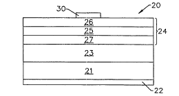
Figure 1 schematically illustrates a vertical
sectional view of a first embodiment of an extended
lifetime light emitting diode according to the present
invention;
2
2 00 305
_$_
' Figure 2 schematically illustrates a vertical
sectional view of a second embodiment of an extended
lifetime light emitting diode according to the present
invention;
Figure 3 schematically illustrates a vertical
sectional view of a third embodiment of an extended
lifetime light emitting diode according to the present
invention;
Figure 4 schematically illustrates a vertical
sectional view of a fourth embodiment of an extended
lifetime light emitting diode according to the present
invention; .
Figure 5 graphically illustrates relative
intensity over time of a prior art light emitting diode
in comparison to a light emitting diode according to
the present invention;
Figure 6 graphically illustrates a double
crystal X-ray rocking curve for a GaN layer on a SiC
substrate as used in a light emitting diode according
to the present invention;
Figure 7 graphically illustrates
photoluminescence as compared to energy output of a GaN
layer on a SiC substrate as utilyzed in an extended
lifetime light emitting diode according to the present
invention;
Figure 8 graphically illustrates intensity as
compared to kinetic energy of an alloy of SiC-A1N-GaN;
and
Figure 9 graphically illustrates crystal
lattice peak energy as a function of silicon carbide
concentration in a SiC-A1N-GaN alloy according to the
present invention.
Detailed Description Of A Preferred Embodiment
The present invention is a light-emitting
diode that produces light in the blue portion of the
visible spectrum and that is characterized by an
CA 02200305 1997-07-24
_g_
extended lifetime. As known to those familiar with the
performance, characteristics and ratings of such light-
emitting diodes, the lifetime is generally defined as
the time over which the LED's output will degrade to
about 50% of its original output.
Figure 1 is a cross-sectional schematic view
of a light-emitting diode according to the present
invention and generally designated at 20. The diode
comprises a conductive silicon carbide substrate 21
which, in preferred embodiments, is a single crystal
silicon carbide substrate. As is well understood by
those of ordinary skill in this art, a high quality
single crystal substrate provides a number of
structural advantages that in turn provide significant
performance and lifetime advantages. In preferred
embodiments, the SiC substrates can be formed by the
methods described in U.S. Patent No. 4,866,005 (now No.
RE 34,861) which is commonly assigned with the pending
application.
An ohmic contact 22 is made to the silicon
carbide substrate and is one of the characteristics of
the present invention that immediately distinguishes it
from prior diodes of the materials discussed herein.
As noted earlier, the typical substrate for gallium
nitride is sapphire, which cannot be made conductive,
and thus cannot be connected to an ohmic contact. This
prevents a sapphire-based device from being formed in
the vertical structure that is most preferred for LEDs
and many other devices.
Figure 1 further illustrates that the LED 20
comprises a buffer layer 23 on the substrate 21. The
buffer layer 23 is selected from the group consisting
of gallium nitride, aluminum nitride, indium nitride,
ternary Group III nitrides having the formula A,~B1_,~N,
where A and B are Group III elements and where x is
zero, one or a fraction between zero and one,
quaternary Group III nitrides having the formula A,~BYCl_X-
AMENDED ~aHEt1
22 00 305
-lo-
y,N where A, B, and C are Group III elements, x and y,
are zero, one, or a fraction between zero and one, and
1 is greater than (x + y) and alloys of silicon carbide
with such ternary and quaternary Group III nitrides.
The buffer layer 23 and the substrate 21 are both
conductive.
The LED 20 further includes a double
heterostructure designated by the brackets 24, and
specifically including a p-n junction, on the buffer
layer 23. The structural desianation "double
heterostructure" is used in a manner common to, and
well understood in, this art. Aspects of these
structures are discussed, for example, in Sze, Physics
of Semiconductor Devices, Second Edition (1981) at
pages 708-710. The Sze discussion on those pages
refers to lasers, but illustrates i=he nature of, and
the distinction between, homostructure, single
heterostructure, and double heterostructure junctions.
In the embodiment illustrated in Figure 1,
the double heterostructure 24 further comprises an
active layer 25 along with upper 2E~ and lower 27
heterostructure layers adjacent the active layer 25.
The heterostructure layers 26 and 27 are preferably
formed of a composition selected from the group
consisting of gallium nitride, aluminum nitride, indium
nitride, ternary Group III nitrides having the formula
AXB1-XIV, where A and B are Group III elements and where x
is zero, one or a fraction between zero and one, and
alloys of silicon carbide with such ternary Group III
nitrides, e.g.,
(SiC) xAyBi_~,N. Stated differently, the lowest
heterostructure layer will be on top of the buffer
layer. In Figure 1, this is illustrated as lower
heterost~ructure 27 being on top of buffer layer 23.
An ohmic contact 30 can be applied to the
upper heterostructure layer 26 to complete the
advantageous vertical structure of the invention. The
~2 00 305
-11-
ohmic contacts preferably are each formed of a metal
such as aluminum (A1), gold (Au), platinum (Pt), or
nickel (Ni), but may be formed of other material for
forming ohmic contacts as understood by those skilled
in the art.
In each of the embodiments illustrated
herein, the double heterostructure comprises an active
layer selected from the group consisting of gallium
nitride, aluminum nitride, indium nitride, ternary
Group III nitrides having the formula AXB1_XN, where A
and B are Group III elements and where x is zero, one
or a fraction between zero and one, and alloys of
silicon carbide with such ternary Group III nitrides.
In the heterostructure 24 illustrated in
Figure 1, the active layer 25 can preferably comprise
indium gallium nitride and the upper and lower
heterostructure layers 26 and 27 will preferably
comprise aluminum gallium nitride. More specifically,
the aluminum gallium nitride heterostructure layers 26
and 27 preferably have the formula AlXGa1_XN where x is
zero, one or a fraction between zero and one. When the
active layer.25 comprises indium gallium nitride, the
composition will be understood to be InZGal_ZN, where z
is a fraction between zero and one.
As known to those of ordinary skill in this
art, the composition of the ternary Group III nitrides
can affect both their refractive index and their
bandgap. Generally speaking, a larger proportion of
aluminum increases the bandgap and decreases the
refractive index. Thus, in preferred embodiments, in
order for the heterostructure layers 26 and 27 to have
a bandgap larger than the active layer 25 and a
refractive index smaller than the active layer 25, the
layers 26 and 27 have a higher atomic or mole
percentage of aluminum than.does the active layer 25.
The larger bandgap of the heterostructure layers 26 and
27~encourages electrons to be injected through the
22 00 305
-12-
active layer 25 thus increasing the efficiency of the
device. Similarly, the lower refractive index of the
heterostructure layers 26 and 27 encourage the light to
be more preferably emitted on an optical basis from
active layer 25.
In order to form the p-n. junction, the upper
and lower heterostructure layers 26 and 27 have
opposite conductivity types from one another, and the
active layer 25 has the.same conductivity type as one
of the two heterostructure layers. For example, in a
preferred embodiment, the upper heterostructure layer
26 is p-type, the active layer 25 is n-type, the lower
heterostructure layer 27 ,is n-type, and the buffer and
the silicon carbide substrate are both also n-type.
The p-n junction is thus formed between the active
layer 25 and the upper heterostructure layer 26.
Figure 2 illustrates a slightly different
embodiment of the present invention broadly designated
at 32. As in the previous embodiment, the LED
comprises a silicon carbide substrate 33 and its ohmic
contact 34. The double heterostructure is designated
by the brackets at 35. In the embodiment of Figure 2,
the buffer layer is shown at 36 and comprises gallium
nitride, and the overall structure further comprises a
gallium nitride epitaxial layer 37 on the buffer layer
between the gallium nitride buffer layer 36 and the
double heterostructure 35. An ohmic contact 40 to the
double heterostructure 35 completes the advantageous
vertical structure of the device.
.30 Although specific performance parameters will
be discussed later herein, the diodes described herein
and illustrated in these and the remaining drawings are
expected to have lifetimes of greater than 10,000 hours
operating at a forward bias current of 50 milliamps at
room temperature, and lifetimes of greater than 10,000
hours operating at a forward bias current of 30
milliamps at room temperature. It will be recognized
22 00 305
-13-
by those familiar with such devices that these
specifications greatly exceed those of presently
available devices.
Figure 3 illustrates a third embodiment of
the present invention broadly designated at 42. As in
the previous embodiments, the diode 42 includes a
silicon carbide substrate 43, and an ohmic contact 44
to the substrate 43. The double heterostructure is
again designated by the brackets 45 and an upper ohmic
contact 46 is made to the double heterostructure 45.
In this embodiment, however, the buffer layer comprises
first and second layers 47 and 48 respectively. The
first layer 47 is on the substrate 43 and is formed of
a graded composition of silicon carbide aluminum
gallium nitride (SiC),~AlYGal_~,N in which the portion
adjacent the substrate 43 is substantially entirely
silicon carbide and the portion furthest from the
substrate is substantially entirely aluminum gallium
nitride, with the portions therebei=weep being
progressively graded in content from predominantly
silicon carbide to predominantly aluminum gallium
nitride.
The second layer 48 is on the first layer 47
and is formed of another graded composition of aluminum
gallium nitride. In preferred embadiments, the
composition of the graded second layer 48 is graded
from a composition matching the composition of the
first buffer layer 47 at the point where the layers 47
and 48 meet, to a composition matching the composition
of the lowest layer of the double heterostructure 45.
With respect to Figure 3, the buffer layer
can also be described as having at least one graded
layer of silicon carbide and a Group III nitride in
which the graded layer is silicon carbide at the
interface with the substrate and then progressively
graded to a composition matching the composition of the
,
22 00 305
-14-
lowest layer of the double heterostructure at the
interface with the double heterostructure.
The invention can further comprise a strain-
minimizing contact layer (not shown) above the active
layer in the double heterostructure and that would have
a lattice constant substantially the same as the
respective buffer layers. Such a strain-minimizing
contact layer is set forth in an application filed
concurrently herewith by Edmond and Bulman for "Low
Strain Laser Structures with Group III Nitride Active
Layers," which is commonly assigned with this
application and which is incorporated entirely herein
by reference. Briefly summarized, the overall strain
of such a multi-layered crystalline device is a
function of the average of the individual strains based
on the differences between their lattice constants.
Thus, by adding a layer with a lattice constant
substantially the same as the buffer, the weighted
average of the strains becomes more consistent and thus
reduces the overall strain.
As some additional details, the upper surface
of the silicon carbide substrate in any of the
embodiments can be doped with aluminum to enhance the
crystal growth. As already stated, the substrate and
the buffer layers in each embodiment are conductive,
and this is usually accomplished by doping each of the
layers with appropriate dopants. The silicon carbide
substrate can be selected from several of the silicon
carbide polytypes specifically including 3C, 4H, 6H,
and 15R.
Figure 4 illustrates another embodiment of
the present invention broadly designated at 50. The
LED 50 is formed on a silicon carbide substrate 51 upon
which a buffer layer designated by the brackets 52 is
formed. The buffer layer is selected from the group
consisting of gallium nitride, aluminum nitride, indium
nitride, ternary Group III nitrides having the formula
~2 00 305
-15-
A,~B1_,~N, where A and B are Group III elements and where x
is zero, one or a fraction between zero and one, and
alloys of silicon carbide with such ternary Group III
nitrides. A first Group III nitride layer 53 is formed
on the buffer 52 and has a first conductivity type. A
second Group III nitride layer 54 is formed on the
first Group III nitride layer 53 and has a second
conductivity type so that the first and second Group
III nitride layers 53 and 54 form a p-n junction
device. An ohmic contact 55 is made to the second
Group III nitride layer 54, and an ohmic contact 56 is
formed on the silicon carbide substrate.so that a
current supplied across the first and second ohmic
contacts to the p-n junction device produces a high
light intensity output therefrom.
As indicated by the dotted line in Figure 4,
the buffer 52 preferably comprises a first layer 57 on
the substrate 51 and formed of a graded composition of
silicon carbide aluminum gallium nitride in which the
portion adjacent the substrate is substantially
entirely silicon carbide and the portion furthest from
the substrate is substantially entirely aluminum
gallium nitride with the portions therebetween being
progressively graded in content from predominantly
silicon carbide to predominantly aluminum gallium
nitride.
A second buffer layer 58 is upon the first
layer 57 and is formed of a graded composition of
aluminum gallium nitride. As described with respect to
earlier embodiments, the composition of the graded
second layer 58 is progressively graded from a
composition matching the composition of the first
buffer layer 57 at the point where layers 58 and 57
join, to a composition matching the composition of the
lower Group III nitride layer 53 of the diode.
In the diode 50 illustrated in Figure 4, the
nitride layers 53 and 54 are selected from the group
.
2.2 00 305 -
-16-
consisting of gallium nitride, aluminum nitride, indium
nitride, ternary Group III nitrides having the formula
AXB1-XN, where A and B are Group III elements and where x
is zero, one or a fraction between zero and one, and
alloys of silicon carbide with such ternary Group III
nitrides. It will thus be understood that in this and
the previous embodiment, the junction can be a
homostructure, a single-heterostructure, or a ~double-
heterostructure.
The buffer 52 can alternatively comprise a
lower intermediate layer 57 formed. of silicon carbide
positioned on the silicon carbide substrate 51 and an
upper intermediate layer 58 formed of a nitride alloy
positioned on the lower intermediate layer 57.
. The buffer can include at least one graded
layer of silicon carbide and a Group III nitride in
which the graded layer is silicon carbide at the
interface with the substrate 51, and the graded layer
is a composition matching the composition of the lowest
layer of the active device at the interface with the
junction structure.
As in earlier embodiments, the light-emitting
diode can have the upper surface of the silicon carbide
substrate doped with aluminum.
As discussed with reference to some of the
other figures herein, the characteristics of the
crystals according to the present invention are
generally superior to any exhibited by any prior
devices. Thus, a double crystal x-ray rocking curve
for GaN grown on SiC substrates according to the
present invention has a full width half maximum of
about 85 arcseconds (Figure 6).
As noted above, the lifetime of an LED is
defined by the LED degradation time to a light emitting
output of only about 50% of the initial light emitting
output of the LED. As set forth above, Figure 5
graphically illustrates relative intensity over time of
~2 00 305
-1~-
a prior art LED formed of GaN on sapphire as compared .
to an LED according to the present invention. Figure 5
best illustrates the significant improvement of the
lifetime of an LED according to th.e present invention.
The devices were burned in at 50 milliamps.
As illustrated in Figure 5, after an extended
period of time of supplying current to an LED according
to the present invention, as much as 10,000 or more
hours, the LED continues to emit.a high intensity light
output, i.e., greater than about 900 of the initial
light intensity output, and much greater than the about
550 of the initial light intensity output exhibited by
the GaN on sapphire LED after as little as 1000 hours
burn-in. In Figure 5, the dotted line predicts the
performance of GaN on SiC based on the well-established
performance of SiC on SiC.
Nitride alloys are often difficult to grow
two-dimensionally on silicon carbide using conventional
technology, primarily because of the difference in the
surface energy between the two kinds of materials.
More specifically, conventional growth techniques at
relatively high temperatures (i.e., higher than about
1000°C) tend to cause three-dimensional growth on the
upper surface of the silicon carbide substrate. This
three-dimensional growth occurs to such an extent as to
form small individual islands of semiconductor material
on the upper surface of the substrate with a poor
surface coverage. Further growth of these islands is
still three-dimensional, and results in very rough as-
grown surface of nitride alloys. At relatively low
temperatures, i.e., less than 1000°C, however, much
smaller islands of nitride alloys with much higher
density can be grown on the surface~of the silicon
carbide substrate. After a very short period of
further growth at the conventional growth temperatures,
these islands coalescence and cover almost all the
upper surface of the substrate. Further growth on this
~~ 00 305
-18-
surface is the growth of nitride alloys on nitride
alloys and is dominated by two-dimensional lateral
growth. This results in specular as-grown surface of
the film and high electrical and structural quality of
the nitride alloys. The p-n junction device of a Group
III nitride is then formed on the gallium nitride layer
using techniques such as chemical vapor~deposition
(CVD) or molecular beam epitaxy (MBE); see- e.g.,
commonly assigned U.S. Patent No. 5,210,051.
Figures 6-9 illustrate various other
performance and construction characteristics of an
extended lifetime LED according to the present
invention. More particularly, Figure 6 graphically
illustrates a double crystal X-ray rocking curve, i.e.,
counts per second as compared to angle, for a GaN layer
on a SiC substrate according to the present invention.
An analysis of the angular position, intensity, and
peak width of x-ray beams diffracted by crystalline
material provides information on the crystal structure
of the material. In this example, the full width half
maximum (FWHM) for the base GaN of an LED according to
the present invention was found to be about 85
arcseconds. Because the X-ray rocking curve
measurements indicate that the crystal quality of the
GaN on SiC substrate are relatively high, resulting LED
are expected to provide the high intensity, and long
lifetime characteristics that are desired.
Figure 7 graphically illustrates luminescence
as compared to energy output of the base GaN on SiC of
an extended lifetime LED according to the present
invention. The graph illustrates the results of
photoluminescence measurements at an excitation of 325
nm, and a temperature of 295 K. Uniform emission was
observed across the surface.. Room temperature
photoluminescence shows that the emission is dominated
by the band edge exiton at 3.41 eV which is typically
dominated by the defect peak at 2.2 eV for layers grown
2~
00 305
-19-
on sapphire, again indicating the h~.c~t~ quality of GaN
on SiC substrates according to the present invention. -
Figure 8 is an Auger electron spectrum
showing that an alloy layer according to the present
S :~zaver~t.ion contained all five elements i.n t~<e :~~.~'-..~-
GaN alloy: Si, C, Al, N and Ga.
Cathodo7.uminescense measurements ware performed ~t:~ Sr~--
A1N-GaN alloy layers at about 80° Kelvin (K) anc~ showed
several peaks in the ultraviolet (UV) and violet
regions.
Figure 9 graphically illustrates the
resulting edge peak energy as a function of silicon
carbide concentration for these layers according to the
present invention. As shown, the photon energy for the
edge peak depends on the SiC concentration in the alloy
layer. For a layer with a SiC concentration of about
10 mole%, the edge peak was detected at a wavelength of
about 300 nm.
In the drawings and specification, there has
been disclosed typical preferred embodiments of the
invention and, although specific terms are employed,
the terms are used in a generic and descriptive sense
only and not for the purposes of limitation. The
invention has been described in considerable detail
with specific reference to various preferred
embodiments. It will be apparent, however, that
various modifications and changes can be made within
the spirit and scope of the invention as described in
the foregoing specification and defined in the appended
claims.