Note: Descriptions are shown in the official language in which they were submitted.
- 1 -
TN-E027
LIQUID CRYSTAL DISPLAY LEMEN WITH A
TRANSPARENT L CTRODE SU STRATE~ ANL
~,HE TRANSPA ENT EL CTRO E SUB T TE
BACKGROUND OF THE INVENTION
1. Field of the invention
The present invention relates to a liquid
crystal display element having a transparent electrode
substrate excellent in optical isotropy, smoothness,
durability, chemical or solvent resistance, water
moisture barriex properties, gas barrier properties,
flexibility and so on. The present invention also
relates to such a transparent electrode substrate,~which
is suitable not only for a liquid crystal display (LCD)
element, but also for a touch panel, a photosensitive
conductor, a planar phosphor, an organic
electroluminescence element or the like.
2. Description of the Related Art
Recently, portable information apparatus such
as a pager, a portable telephone, an electronic notebook
and a portable information terminal have become popular
and the business and the life style are going to be
dorastically changed, To improve the portability of the
information apparatus, it is demanded to make the
information apparatus thinner, lighter and more durable.
Conventionally, a glass substrate which i.s
heavy, thick and fragile~has been used for a transparent
electroconductive substrate of an LCD element or a touch
panel. As an alternate material, a transparent resin
substrate has been proposed, and the transparent resin
substrate is advantageous in decreasing cost for
manufacturing an LCD and the like since it can be
processed in a roll-to-roll system. However, the
transparent resin substrate is inferior to the glass
substrate in durability, chemical or solvent resistance,
gas barrier properties and other basic properties.
- 2 -
Fox example, in the case of a transparent resin
substrate used as an electrode for a LCD element, the gas
barrier property can be improved by providing a metal
oxide layer to the transparent resin substrate. However,
S there are problems that in the step of removing a resist
after patterning the transparent electrode, the metal
oxide layer contacts an alkali solution by which the
metal oxide layer is dissolved, and in the step of
forming a liquid crystal alignment layer, a coating
composition for the liquid crystal alignment layer
containing N-methylpyrolidone or other solvent is used
and the transparent resin substrate in contact with the
solvent is damaged or, for example, becomes white or
swollen.
To solve the above problems, there are some
proposals of laminating a layer having a gas barrier
property and a chemical resistance onto the transparent
resin substrate. For example, Japanese Examined Patent
Publication (Kokoku) Nos, S-52002 and 5-52003 propose a
transparent substrate comprising a polymer film and an
oxygen gas barrier layer made of polyvinyl alcohol which
has an improved adhesivity and further a moisture barrier
property. however, the polyvinyl alcohol-based polymer
layer disposed as the outermost layer does not have a
sufficient chemical resistance and therefore causes
problems during manufacturing a liquid crystal cell. The
chemical resistance may be given by additionally
providing a chemical resistant layer, which however
increases the cost.
Japanese Unexamined Patent Publication (Kokai)
rlos. 2-137922 and 5-309794 propose a transparent
substrate comprising a transparent polymer film, an
anchor layer, a gas barrier layer made of ethylene-vinyl
alcohol copolymer and a solvent-resistant layer in this
order as a stack. In this transparent substrate, the
solvent-resistance is satisfactory but the gas barrier
property at a high humidity is lowered due to the
- 3 -
property of the material of the gas barrier layer, and
the structure of the six layers increases manufacturing
cost.
Further, in a transparent substrate of a liquid
crystal display element, the following demands on and
problems of the properties exist in addition to the above
chemical resistance and gas barrier properties.
If the substrate is low in its transparency or
has a birefriqence, the coloring of the display and
lowering of contrast occur.
If the surface smoothness of the substrate is
low, the gap for a liquid crystal layer becomes non-
unzform and the liquid crystal orientation may be
disordered or the substrate may become optically non-
uniform. As a result, the displaying color becomes non-
uniform.
Moreover, if the smoothness, transparency, and
gas barrier properties of the substrate are deteriorated
by mechanical or thermal influence or by contact with a
solvent, the advantages of the lightness, the wide range
of the freedom of shape and the possibility of a curved
display can not be obtained in applications to a pager, a
portable telephone, an electronic notebook, a pen-input
apparatus and so on since they receive substantial outer
mechanical or thermal influences. In particular,
considering the resistance to the mechanical influence,
excellent adhesion between the layers is required to
maintain the above advantageous properties.
xhe object of the present invention is to
provide a liquid crystal display element having a
transparent resin substrate which is excellent in the
chemical or solvent resistance, gas barrier properties,
transparency, smoothness, adhesivity and so on as
mentioned above and which has a small number of laminated
layers and thus is low in manufacturing cost.
SUMMARY OF THE INVENTION
The above and other objects and the features of the
- 4 -
present invention are attained by providing:
(I) A liquid crystal display element comprising two
electrode substrates between which a liquid crystal layer
is disposed, at least one of said electrode substrates
S comprising the following components:
A) a metal oxide layer,
B) a cured polymer layer contiguous to said
metal oxide layer, said cured polymer layer being
obtained from a cross-linking reaction of:
B1) a silicon compound having epoxy and
alkoxysilyl groups, a full or partial
hydrolysis product thereof, a full or partial
condensation product thereof, or a mixture
thereof:
B2) a silicon compound having amino and
alkoxysilyl groups, a full or partial
hydrolysis product thereof, a full or partial
condensation product thereof, or a mixture
thereof; and
B3) a polyvinyl alcohol-based polymer;
C) a transparent electroconductive layer; and
D) a transparent polymer substrate with a
retardation of not more than 30 nm for a wavelength of
590 nm;
wherein said transparent electroconductive
layer (C) is formed on the liquid crystal layer side of
said transparent polymer substrate (D), and said
combination of said metal oxide layer (A) and said cured
polymer layer (B) is disposed between said transparent
electroconductive layer (C) and said transparent polymer
substrate D) or is disposed on a side opposite to the
transparent electroconductive layer (C) of said
transparent polymer substrate (D).
(IZ) A liquid crystal display element comprising two
electrode substrates between which a liquid crystal layer
is disposed, at least one of said electrode substrates
comprising the following components:
-5_
A) a metal oxide layer,
B) a cured polymer layer contiguous to said
metal oxide layer,
C) a transparent electroconductive layer, and
S D) a transparent polymer substrate with a
retardation of not more than 30 nm for a wavelength o~
590 nm, wherein said transparent electroconducti.ve
layer (C) is formed on the liquid crystal layer side of
said transparent polymer substrate (D), and said
combination of said metal oxide layez (A) and said cured
polymer layer (B) is disposed between said transparent
electroconductive layer (C) and said transparent polymer
substrate (D) or is disposed on a side opposite to the
transparent electroconductive layer (C) of said
transparent polymer substrate (D),
said cured polymer layer comprising a polyvinyl
alcohol-based polymer cross-linked with a unit
represented by the following formula (3):
~O-Si-(CpHzp)_''lA<.Z~~~Bf~~-(CQH~~)'-Si-~ (3)
where p is an integer of 0 to 5,
q is an integer of 0 to S;
A stands fox
*1,
R' RB
*1 ~ ~ *2 ~~ *2
-f O~jz-CH-CH-CH~- ,
0 0
where R' and Rg are independently hydrogen,
methyl, ethyl or phenyl, and 1 is 0 or 1;
B stands for
*3 ~ J *4
--(.N'~CHz r s N-
Where r is an integer of 0 to 5, and s is
an integer of 0 to 2; and
~v ru
-s-
*2 and *3 are sites bonded each other.
(III) A transparent electrode substrate comprising
the following components:
A) a metal oxide layer,
B) a cured polymer layer contiguous to said
metal oxide layer, said cured polymer layer being '
obtained from cross-linking reaction of:
B1) a silicon compound having epoxy and
alkoxysilyl groups, a full or partial
hydrolysis product thereof, a full or partial
condensation product thereof, or a mixtuze
thereof;
B2) a silicon compound having amino and
alkoxysilyl groups, a full or partial
J.5 hydrolysis product thereof, a full or partial
condensation product thereof, or a mixture
thereof; and
83) a polyvinyl alcohol-based polymer;
and
C) a transparent electroconductive layer; and
D) a transparent polymez substrate with a
retardation of not more than 30 nm for a wavelength of
590 nm;
wherein said combination of said metal oxide
layer (A) arid said cured polymer layer (B) is disposed
between said transparent electroconductive layer (C) and
said transparent polymer substrate (D) or is disposed on
a side opposite to the transparent electroconductive
layer (C) of said transparent polymer substrate
(IV) A transparent electrode substrate comprising
the folJ.owing components:
A) a metal oxide layer,
B) a cured polymer layer contiguous to said
metal oxide layer,
C) a transparent electroconductive layer, and
D) a transparent polymer substrate with a
retardation of not more than 30 nm for a wavelength of
590 nm, wherein said combination of said metal oxide '
layer (A) and said cured polymer layer (e) is disposed
between said transparent electxoconductive layer (C) and
said transparent polymer substrate (D) or is disposed on
a side opposite to the transparent electroconductive
layer (C) of said transparent polymer substrate (D),
said cured polymer layer comprising a polyvinyl
alcohol-based polymer cross-linked with a unit
represented by the following formula (3):
-0-S i-( CyHzp ) ~~.lA,~z~w3 B"<_ ( CqHZq ) _S i-0- ( 3 )
where p is an integer of 0 to S,
q is an integer of 0 to S;
A stands for
*1
1 S R' R8
*1 ~ ~ *Z ~ *2
--f 0 j-rCH-CH-~H- ,
0 0
where R' and R8 are independently hydrogen,
methyl, ethyl or phenyl, and 1 is 0 or l;
B stands fox
ZS *3 f ~ *4
-j-N~'CHz r s N-
where r is an integer of 0 to 5, and s is
an integer of 0 to 2; and
*2 and *3 axe sites bonded each other.
(V) An article comprising:
D) a substrate; and
8) a cured polymer layer formed on a surface
of said substrate, said cured polymer layer being
obtained from cross-linking reaction of:
B1) a silicon compound having epoxy and
alkoxysilyl groups, a full or partial
hydrolysis product thereof, a full or partial
condensation product thereof or a mixture
thereof;
~',~~''~~"
_ g _
B2) a silicon compound having amino and
alkoxysilyl groups, a full or paztial
hydrolysis product thereof, a full or partial
condensation product thereof yr a mixture
thereof; and
B3) a polyvinyl alcohol-based polymer.
(VI} A process for producing a coated article,
comprising the steps of:
a) preparing a coating composition which
l.0 comprises
B1) a silicon compound having epoxy and
alkoxysilyl groups, a full or partial
hydrolysis product thereof, a full or partial
condensation product thereof or a mixture
thereof;
B2) a silicon compound having amino and
alkoxysilyl groups, a full or partial
hydrolysis product thereof, a full or partial
condensation product thereof or a mixture
thereof;
B3) a polyvinyl alcohol-based polymer;
B4) a carboxylic acid;
BS) an organic solvent; and
B6) water;
b) coating a substrate with said coating
composition; and
c) curing said coating composition by cross-
linking reaction between said compounds (B1) to ($3) to
form a cured polymer layex on said substzate.
(VII) A coating composition which comprises:
B1) a silicon compound having epoxy and
alkoxysilyl groups, a full or partial
hydrolysis product thereof, a full or partial
condensation product thereof or a mixture
thereof;
B2) a silicon compound having,amino and
alkoxysilyl groups, a full or partial
- 9 -
hydrolysis product thereof, a full ox partzal
condensation product thereof or a mixture
thereof;
B3) a polyvinyl alcohol-based polymer;
B4) a carboxylic acid;
BS) an organic solvent; and
B6) water.
BRIEF DESCRIPTIONS OF DRAWINGS
Fig. 1 is a cross-sectional view of an example of a
liquid crystal display element;
Fig. 2 shows a cross-sectional view of a
commercially available transparent polymer electrode
substrate;
Fig. 3 schematically shows the reaction of a hybrid
of a polyvinyl alcohol-based polymer with an
alkoxysilane;
Figs. 4A and 4B show the oxygen permeation property
of gas barrier layers;
Fig. 5 is a cross-sectional view of a lamination of
a gas barrier layer of a hybrid and SiOX layers with a
polycazbonate film;
Figs. 6A to 6C show the combined effect of the
hybrid and SiOz layers;
Fig. 7 shows the alkali resistance of hybrid layers;
Fig. 8 schematically shows the reactions between the
compounds (B1) to (B3);
Fig. 9 shows a cross section of an ideal transparent
polymer substrate in accordance with the present
invention;
Figs. 10A to lOD and 11A to 11F show various
arrangements of the components (A) to (D) of the present
invention.
DESCRIPTION OF THE PREFERRED EMBODIMENTS
Liqui Czvstal Display Element
The liquid crystal display element is a display
element in which a liquid crystal material is sealed
- 10 -
between two substrates having an electrode pattern and an
voltages are applied between the electrodes sv as to
electro-optically modulate the liquid crystal material
and make a display such as of letters and images. The
substrate of the liquid crystal display element is
conventionally an inorganic glass but a liquid crystal
display element using a plastic substrate is attracting
attention from the viewpoints of making the element
thinner and lighter, allowing a curved display, providing
strength, and reducing production cost.
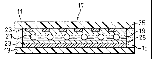
Fig. 1 is an illustration of an example of a liquid
crystal display element, in which an upper substrate 11
and a lower substrate i3 are disposed to face each other,
the peripheries of the substrates 11 and i3 are sealed
with a sealing maternal 15, a gapping maternal 21 is
dispersed between the substrates 11 and 13, and a liquid
crystal cell 17 is thus formed, in which a liquid cxystal
material 19 zs filled. Polarizing plates axe provided
sandwiching the cell 17 to form a TN-type liquid crystal
display element, although the present invention is not
limited to this type of the liquid crystal display
element.
Each of the upper and lower substrates 11 and 13
has, on the inner side, a transparent electroconductive
layer 23 and an aligning layer thereon.
Fig. 2 shows a cross-sectzon of a transparent
polymer electrode substrate whzch is commercially
available. The transparent polymer electrode substrate
comprises a polycarbonate film 1, anchor layers 2, gas
barrier layers of an ethylene-vinyl alcohol copolymer 3,
solvent-resistant layers 4 and a transparent
electroconductive layer of ITO 4, The polycaxbonate
film 1 is about 100 um thick and the other layers 2 to 4
are a few um thick.
The liquid crystal display element of the present
invention comprises two electrode substrates, at least
one of Which comprises a metal oxide layer (A}, a cured
- 11 -
polymer layer (B), a transparent electroconductive
layer (C) and a transparent polymer substrate (D).
Transparent Polvmer Substrate fD.~
The transpazent polymer substrate (D) used in the
present invention is not particularly limited as long as
it has an optical isotropy or a retardation of not more
than 30 nm fox a wavelength of 590 nm. The retardation
is represented by a product An~d where ~n stands for a
difference between the refractions of a birefrigence for
a wavelength of 590 nm which can be measured by a
conventional device and d stands for a thickness of the
substrate. If the retardation is more than 30 nm,
coloring and viewangle problems appear. Preferably the
zetardation is not more than 20 nm. The dispersion of
the retardation phase axis is preferably within ~30°,
more preferably within ~15°.
The materials which can satisfy the above
requirements include polyester-based resins,
polycarbonate-based resins, polyarylate-based resins,
polysulfone-based resins such as polysulfone,
polyethersulfone and polyallylsulfone, polyolefin-based
resins, acetate-based resins such as cellulose
triacetate, polystylene-based resins, acrylic resins, and
various thermosetting resins. Among them, a transparent
polymer substrate comprising a polycarbonate-based resin
as a main component is most preferred from the viewpoints
of a high optical transparency and a low optical
anisotropy.
The thickness of the transparent polymer substrate
is usually between 30 um and 800 gym.
Metal pxide Laver ~
The metal oxide layer (A) used in the present
invention may be of an insulating metal oxide such as
oxides of silicon, aluminum, magnesium and zinc. The
transparent insulating metal oxide layer may be deposited
by known spattering, evaporation, ion plating, plasma
enhanced CvD, and so on. Silicon oxide is particularly
- 12 -
preferred as a metal oxide for a water moisture barrier
layer from the viewpoints of transparency, surface
smoothness or evenness, flexibility, layer stress, cost,
etc.
The composition of silicon oxide may be analyzed and
determined by X-ray photoelectron spectroscopic analyzer,
X-ray microspectroscopic analyzer, Auger electron
analyzer, Rutherford back scattering, etc. Silicon oxide
having an average composition represented by SiOx where
1.5 < x < 2 is preferred for its visible light permeation
and flexibility. If the value of x is less than 1.5, the
flexibility and the transparency are lowered. The
silicon oxide having an average composition represented
by SiOx where 1.5 < x ~ 2 may further comprises other
metals such as magnesium, iron, nickel, chromium,
titanium, aluminum, indium, zinc, tin, antimony,
tungsten, molybdenum, copper. The silicon oxide further
may contain fluoride or carbon to increase flexibility.
The amount o~ such additives is not more than 30~ by
weight.
The thickness of the metal oxide layer is preferably
between 2 nm and 200 nm. If the thickness of the layer
is less than 2 nm, it is difficult to form a uniform
layer and the layer formed may have pores from where gas
permeates the substrate, reducing the gas barrier
properties. If the thickness is more than 200 nrn, the
transparency of the layer is lowered and the flexibility
becomes poor causing cracks, thus reducing the gas
barrier properties.
3 0 Cured PoJ.ymer Layer ~( B )
The cured polymer layers (8) used in the present
invention is formed by cross-linking reaction of the
components:
B1) a silicon compound having epoxy and alkoxysilyl
groups, a full or partial hydrolysis product thereof, a
full or partial condensation product thereof, or a
13 -
mixture thereof;
82) a silicon compound having amino and alkoxysilyl
groups, a full or partial hydrolysis product thereof, a
full or partial condensation product thereof, or a
S mixture thereof; and
B3) a polyvinyl alcohol-based polymer.
The cured polymer layer B) is formed in contiguous
to or in contact with the metal. oxide layer.
The component compounds (81) to (B3) are described
below:
polyvinyl Alcohol-Based olymer {B3l
The polyvinyl alcohol-based polymer {B3) of the
present invention may be a known one and is commercially
available. The polyvinyl alcohol-based polymer B3)
preferably comprises not less than SO% by mole of a
polyvinyl alcohol component and/ox a polyvinyl alcohol
cvpolymer component.
Examples of polyvinyl alcohol-copolymers include
vinyl alcohol-vinyl acetate copolymer, vinyl alcohol
vinyl butylai copolymer, ethylene-vinyl alcohol
copolymer, and vinyl alcohol-based alcohol having silyl
groups in its molecule.
Generally, a polyvinyl alcohol-based polymer
selected fzom polyvinyl alcohol having a degree of
saponification of not less than 80~, ethylene-vinyl
alcohol copolymer and polyvinyl alcohol-based polymer
having silyl groups in its molecule is preferred.
The ethylene content in the ethylene-vinyl alcohol
copolymer is preferably not more than SO%. If the
ethylene content is more than 50%, a desired gas barrier
property of the cured polymer layer can not be obtained.
The polyvinyl alcohol-based polymer having silyl
groups in its molecule is one having a reactive silyl
group represented by the following formula (4):
{R110)= Si-
yz (4)
(R )s_x
- 14 -
where R11 stands for hydrogen, alkyl. having 1 to 10
carbon atoms, acyl, an alkali metal or an alkali earth
metal, Rli stands for alkyl having 1 to 10 carbon atoms,
and r is an integer of 1 to 3.
The silyl group in the molecule may be a terminal
group of the polyvinyl alcohol-based polymer. The site,
distribution, etc. of the silyl. group in the molecule are
not limited as long as the silyl group is bonded to the
polyvinyl alcohol-based polymer through a non-
hydrolyzable bond. The content of silyl is preferably
not more than 5% by mole, more preferably not more than
1% by molar. If the silyl content is too high, the
coating composition becomes disadvantageously viscous and
tends to be geled.
The polymerization degree and saponification degree
of the polyvinyl alcohol-based polymer of the present
invention are not particularly limited but the average
polymerization degree is preferably between 100 and 5000
and the saponi~ication degree is preferably not less than
70~, more preferably not less than 80%. If the
polymerization degree is too low, the coated layer is
brittle. If polymerization degree is too high, the
coating solution becomes too viscous and coating is
difficult. If the saponification degree is too low, a
sufficient gas barrier property is not obtained.
S>>s~on Compound Having Egoxy And Alkoxys~lyl G~ups
B1
The compound (B1) of the present invention is a
silicon compound having epoxy and alkoxysilyl groups, a
full or partial hydrolysis product thereof, a full or
partial condensation product thereof, or a mixture
thereof. A preferable silicon compound having epoxy and
alkoxysilyl groups is represented by the following
formula (1):
3 5 ~Zn
1 ~ ~ ~1)
X-R --S i ( OR ) 3-"
- 15 -
where R1 is alkylene having 1 to 4 carbon atoms,
RZ and R3 are independently alkyl having 1 to 4
carbon atoms,
X is glycidoxy oz epoxycyclohexyl, and
n is 0 or 1.
Examples of the above silicon compound having epoxy
and alkoxysilyl groups (B1) include
glycidoxymethyltximethoxysilane,
glycidoxymethyltriethoxysilane,
glycidoxymethyltripropoxysilane,
glycidoxymethyltributoxysilane,
2-glycidoxyethyltrimethoxysi.lane,
2-glycidoxyethyltriethoxysilane,
2-glycidoxyethyitripropoxysilane,
2-glycidoxymethyltributoxysilane,
1-glyci.doxyethyltrimethoxysilane,
1-glycidoxyethyltri.ethoxysilane,
1-glycidoxyethyltripropoxysilane,
1-glycidoxymethyltributoxysilane,
3-glycidoxypropyltrimethoxysi.lane,
3-glyci.doxypropyltriethoxysilane,
3-glycidoxypropyltripropoxysilane,
3-glycidoxypropyltributoxysilane,
1-glycidoxypropyltrimethoxysilane,
1-glycidoxypropyltriethoxysilane,
1-glycidoxypropyltripxopoxysilane,
1-glycidoxypropy7.tributoxysilane,
(3,4-
epoxycyclohexyl)methyltrimethoxysilane,3,4-
epoxycyclohexyl)methyltriethoxysilane,(3,4-
epvxycyclohexyl)methyltripxopoxysilane,(3,4-
epoxycyclohexyl)methyltributoxysilane,2-(3,4-
epoxycyclohexyl)ethyltrimethoxysilane,2-(3,4-
epoxycyclohexyl)ethyltrzethoxysilane,-(3,4-
2
epoxycyclohexyl)ethyltripropoxysilane,2-(3,4-
epoxycyclohexyl)ethyltributoxysilane,-(3,4-
3
epoxycyclohexyJ.)propyltrimethoxysxlane,3-(3,4-
- 16 -
epoxycyclohexyl)propyltriethoxysilane, 3-(3,4-
epoxycyclohexyl)propyltripropoxysilane, 3-(3,4-
epoxycyclohexyl)propyltributoxysilane, 4-(3,4-
epoxyCyclohexyl)butyltrimethoxysilane, 4-(3,4-
epoxycyclohexyl)butyltriethoxysilane, 4-(3,4-
epoxycyclohexyl)butyltripropoxysilane, 4-(3,4-
epoxycyclohexyl)butyltributoxysilane, diethoxy-3-
glycidoxypropylmethylsilane, etc.
Particularly preferred silicon compounds having an
epoxy and alkoxysilyl groups (B1) are 3-
glycidoxypxopyltrimethoxysilane and 2-(3,4-
epoxycyclohexyl)ethylt~rimethoxysilane.
The above silicon compounds may be used alone or in
combination.
i5 Silicon Compound Havina Amino And Alkoxysilyi Groups
(B2)
The compound (B2) of the present invention is a
silicon compound having amino and alkoxysilyl groups, a
full or partial hydrolysis product thereof, a full or
partial condensation product thereof, or a mixture
thereof. A preferable silicon compound having amino and
alkoxysilyl groups is represented by the following
formula (2):
X R5~
as ~ ~ (2)
HN-R '--$ i ( OR6 ) ~ _m
where R' is alkylene having 1 to 4 carbon atoms,
Rs and R6 are independently alkyl having 1 to 4
carbon atoms,
Y is hydrogen or aminoalkyl, and
m is 0 or 1.
Examples of the silicon compounds having amino and
alkoxysilyl groups (B2) include
aminomethyltxiethoxysilane, 2-aminoethyltrimethoxysilane,
2-aminoethyltriethoxysilane, 2-
aminoethyltripropoxysilane, 2-aminoethyltributoxysilane,
1-aminoethyltrimethoxysilane, 1-
- 17 -
aminoethyltriethoxysilane, 3-aminopzopyltrimethoxysilane,
3-aminopropyltriethvxysilane,
3-
ami.nopropyltripropoxysilane,3-
aminopropyltributoxysilane,2-
aminopropyltrimethoxysilane,2-
aminopropyltriethoxysilane,2-
aminopropyltripropoxysilane,2-
aminopropyltributoxysilane,1-
aminopropyltrimethoxysilane,1-
aminopropyltriethoxysilane,1-
aminopropyltripropoxysilane,1-
aminopropyltributoxysilane,N-
aminomethylaminvmethyltriethoxysilane,
N-
aminomethylaminomethyltripropoxysilane,
N-aminomethyl-2-
aminoethyltrimethvxysilane,N-aminomethyl-2-
aminoethyltriethoxysilane,
N-aminomethyl-2-
aminoethyltripropoxysilane,N-aminomethyl-3-
aminopropyltrimethvxysilane,N-aminomethyl-3-
aminopropyltriethoxysilane,N-aminomethyl-3-
aminopropyltripropoxysi.lane,N-aminomethyl-2-
aminopropyltrimethoxysil.ane,N-aminomethyl-2-
aminopropyltriethoxysilane,r1-aminomethyl-2--
aminopropyltripropoxysilane,N-
aminopropyltrimethoxysilane,N-
aminopropyltriethoxysilane,N-(2-aminoethyl)-2-
aminoethyltrimethoxysilane,N-(2-aminoethyl)-2-
amznoethyltriethoxysilane,
N-(2-aminoethyl)-2-
aminoethyltripropoxysilane,N-(2-aminoethyl)-1-
aminoethyltrimethoxysilane,N-(2-aminoethyl)-1-
aminoethyltriethoxysilane,
N-(2-aminoethyl)-1-
aminoethyltripropoxysilane,N-(2-aminoethyl)-3-
aminopropyltriethoxysilane,N-(2-aminoethyl)-3-
aminoprvpyltripropoxysilane,N-(3-aminopropyl)-2-
aminoethyltrimethoxysilane,N-(3-aminopropyl)-2-
aminoethyltriethoxysilane,
N-(3-aminopropyl)-2-
aminoethyltripropoxysilane,N-methyl-3-
aminopropyltrimethoxysilane,3-
_ is _
ami.nopropylmethyldimethoxysilane, 3-
aminopropylmethyldiethoxysilane, N-(2-aminoethyl)-3-
aminopropylmethyldimethoxysilane, 3-
diethylenetriarninopropyltriethoxysilane, 3-(2-(2-
aminoethylaminoethylamino)propylJtrimethoxysilane,
trimethoxysilylpropyldiethylenetriamine, etc.
Particularly preferred silicon compounds having
amino and alkoxysilyl groups (B2) are 3-
aminopropyltrimethoxysiJ~ane, 3-
aminoprvpyl.triethoxysilane, 3-
aminopropylmethyldiethoxysilane, N-methyl-3-
aminopropyltrimethoxysilane, N-(2-aminoethyl)-3-
aminopropyltrimethoxysilane, and N-(2-aminoethyl)~3--
aminopropylmethyldimethoxysilane.
These silicon compounds having amino and alkoxysilyl
groups may be used alone or in combination.
Hydrolysis and ondensation Products of Compounds
(Blj~d (B21
The full or partial hydrolysis product, or the full
ZO or partial condensation product of the above silicon
compound are obtained through so-called sol-gei reaction
of the silicon compound. the condensation product of the
silicon compound may include not only a condensation
product between the silicon compound but also a
condensation product between an unreacted silicon
compound and a full or partial hydrolysis product of the
silicon compound.
The compounds (B1) and (B2) used as the starting
material may be a silicon compound itself, or a
hydrolysis product or condensation product of a silicon
compound which has been previously prepared.
The hydrolysis of the silicon compound may be
carried out using, for example, an inorganic acid such as
hydrochloric acid, an organic acid such as acetic acid,
or an alkali such as sodium hydroxide, or only water.
The hydrolysis may be carried out after mixing a silicon.
compound and a solvent in order to make the hydrolysis
- 19 -
uniform. Heating or cooling may be effected during the
hydrolysis if necessary. Alternately, a solvent such as
alcohol may be removed after the hydrolysis by heating
and/or evacuation or an appropriate solvent may be
further added.
Cross Linking Reaction
By reacting the above compounds {B1) tv (B3} in
accordance with the present invention, the cured polymer
layer can have a combination of excellent chemical or
solvent resistance, gas barrier properties and adhesivity
in addition to optical isotropy, surface smoothness,
durability, water moisture baxrier properties, a
flexibility and so on.
In this reaction, it is believed that by using a
combination of the silicon compound having epoxy and
alkoxysilyl groups (81) and the silicon compound having
amino and alkoxysilyl gxoups (B2), not only
(1) the reaction between the silanol gXOUps of the
alkoxysilyl groups, but also
(2) the xeaction between the epoxy and amino
groups, and
(3) the reaction between the silanol group of the
alkoxysilyl group and the hydroxy group of the polyvinyl
alcohol-based polymer,
occur as the main reactions. Thus, there is formed a
cured product from a reaction between the two types of
the silicon compounds and a cross-linked product of the
polyvinyl alcohol-based polymer and, as a result, the
reaction product exhibits excellent chemical or solvent
resistance and the other properties,
~~,oss Linked polymer
As a result of the above reaction, it is considered
that the reaction product of the present invention
includes the chemical bond represented by the following
formula (3):
-zo-
-~.-Si-(CpHZp) *lA°Z *~B*~-(CqgZq)-5i.-O- (3)
where p is an integer of 0 to S,
q is an integer of 0 to 5;
A stands for
*1
R~ Ra
*1 ~ ~ *2 ~ *2
-fOj-rCH-CH-CH- ,
p 0
where R' and Ra axe independently hydrogen,
methyl, ethyl or phenyl, and 1 is 0 or 1;
B stands for
*3 ~ ~ *4
-CNfCHz r s N-
where r is an integer of 0 to 5, and s is
an integer of 0 to 2; and
*2 and *3 are sites bonded to each other.
The structure of the main cross-linkages of the
present invention may be the structure comprised only o~
the above formula (3), or may further comprise the
structures as represented by the following formulae (5)
and (6), and the like:
~S1-(-CpFiZp )--~~lA'~Z °3g°4-(-CqFiZq--)-S1-0-S1-
(-CqH29 ) ~38'~'-YlA'~Z-(-CpH2p )-Sl-0- ( 5 )
'~ i% L~,y ~ ~j ~~_t
- 21 -
-o-Si-(-CpHZP ) ~lA~z-~lBa'-(-CqHzq )-5i--0-Si'
(~qHza ) ~j$fr~ ~lA~z-(-~pHzp )-Si-O-Si-
ZO (--CpHZp-)- lA~'? °3B.~'-(-CqHzq-)-S1-O-
where the abrebiations are as defined in the formula (3).
composition of Component (B1
The ratios between the compounds (B1) to (B3) used
preferably satisfy the following formulae:
1/9 <_ (B~)/((B,) + (Bz)] ~ 9/1, by weight, and
1/9 < (bl)/(bz) < 9/1, by mole,
where B1 to Bs stand for the amounts in weight of the
compounds (81) to (B3), respectively; bi stands for the
amount of the compound Bl) based on the mole of the epoxy
group thereof; and bz stands for the amount of the
compound H2) based on the total mole of the amino and
imino groups thereof. More specifically, B1 and Bz axe
calculated based on the weights of the following
compounds (1') and (2'), respectively:
Rz
n
X-R1-SlO~3_n)l2 ( ~ , )
X Rsm
(2~)
HN-R -Si0~3_"yZ
For example, when z00 parts by weight of compound (B1)
represented by the fozmula (1) is used, B1 represents the
weight of the compound having the structure as
represented by the formula (i') which is a full
condensation product and, therefore, 81 is 90 parts by
weight.
If the ratio (B~)/[(B1) + (Bz)) is over 9/1, the
- 22 -
water resistance and chemical resistance tend to be
lowered. If the ratio (Bj)/( (B1) + (BZ) ) is less than
1/9, the gas barrier property decreases. The preferable
range of the ratio (B3)/((B1) + ($z)1 is 2/8 to 8/2, more
prefezably 1/3 to 3/1. When a transparent
electroconductive layer (C) is laminated on a cured
polymer layer (8), 1/9 < (B3)/((BI) * ($z)) < 4/1 is
preferable for adhesion between the layers. when a
silyl-containing polyvinyl alcohol is used, a preferable
ratio (Bs) / ( (B~) -~ (BZ) ] is 2/1 to 1l9 .
Properties of Component lB) nd Combined Effects of
C~ponents ,~A) and lB1
The cured polymer layer (B) obtained by the above
cross-linking reaction has excellent chemical or solvent
resistance, gas barrier properties and adhesivity as well
as other propezties required for a transparent electrode
substrate.
As described before, a polyvinyl alcohol-based
polymer may have a gas barrier property but is
deteriorated With water or at a high humidity atmosphere
and has a poor adhesivity to a polycarbonate or other
polymer substrate and a metal oxide layer. Some of these
defects may be improved by adding a chemical resistant
layer and an anchor layer, but they add manufacturing
costs and the gas barrier property is still not
sufficiently high.
The data shown in the following table are the
properties of transparent polymer substrates, one of
which is the commercially available one based on an
ethylene-vinyl alcohol copolymer-based polymer ("prior
art"). one of which is desired or aimed at the present
("target"), and one of which is obtained by the present
,invention ( invention"). The properties indicated are
measured by the methods as described later in the section
0~ Examples.
- 23 -
TABLE
Properties Prior Art Target Invention
Gas barrier:
OZ (SO%RH) 0.5 <0.2 <0.01
Oz (90%RH) 10.5 <10 <0.05
Chemical resistance:
NMP 2min >3min >Smin
Alkali no change no change no change
Acid no change no change no change
Adhesivity to:
SiOx 0/100 100/100 100/100
Polycarbonate 1001100 100/100 100/100
It is possible that the transparent electrode
substrate has the following excellent chemical resistant
properties:
i) a change of haze value of not more than 1% when
N-methylpyrorydone is put in contact with the cured
polymer layer side of the transparent electrode substrate
at 25°C for 10 minutes followed by cleaning with water;
ii) no deterioration When 3.5%-NaOH aqueous
solution is put in contact with the cured polymer layer
side of said transparent electrode substrate at 25°C for
10 minutes followed by cleaning With water; and
iii) no deterioration when 5.0%-HC1 agueous solution
is put in contact with the cured polymer layer side of
said transparent electrode substrate at 25°C for 10
minutes followed by cleaning with water.
Furthermore, the cured polymer layer (B) can adhere
to both a transparent polymer substrate, particularly
polycarbonate, and a metal oxide layer, particularly
silicon oxide.
As seen in the above table, all of the gas barrier
properties (in cm'/mZ/atm/day), the solvent resistances
and the adhesivity are improved in the present invention.
- 24 -
rt is tv be noted that these improved properties of
the present invention are basically obtained by the
component (B) alone, although the properties of the
commercially available one are obtained by the
combination of the polyvinyl alcohol-based polymer with
the chemical resistant layer and an anchor layer (six
layers 2 to 4 are added as shown in Fig. 2). The gas
barrier property as mentioned above of the present
invention is one obtained by the combination of the
component (8) and a metal oxide layer (A), but addition
of only three layers as shown in Fig. 9 in accordance
with the present invention allows to obtain properties
superior to the properties of the prior art.
As shown in Fig. 3, a polyvinyl alcohol-based
polymer has flexibility and gas barrier properties. By
cross-linking a polyvinyl alcohol-based polymer with an
alkoxysilane to form a hybrid polymer, the chemical
resistance and abrasion resistance are provided to the
hybrid polymer because of the cross-linked polymer has a
microscopically uniformly linked structure.
Further, by selecting the specif~.c silicon compound
(a silane coupler-type compound) as the cross linking
agent, the improvements are increased as described above.
Gas Barrier Property:
Referring to Fig. 4A, the oxygen permeations of gas
barrier layers formed on a polycarbonate film (PC) are
shown. The line indicated as "prior art" is of an
ethylene-vinyl alcohol copolymer. The line indicated as
"H/PC" is of the hybrid layer of a polyvinyl alcohol.
The oxygen permeation of the hybrid layer at a low
humidity is superior to the prior art. The line
indicated as °SiOx/PC" is of the SiOx layer, although
this can be further improved by increasing the thickness
of the SiOx. Here, a lamination of the hybrid layer with
the SiOx layer is theoretically expected to provide an
oxygen permeation as shown by the broken line as
~~~,
- 25 -
indicated by "H/SiOx/pc (theoretical)". However, the
actually measured oxygen permeation of the lamination of
the hybrid layer with the SiOx layer is as shown by the
solid line as indicated by "H/SiOX/PC (measured)", which
is significantly superior to the theoretical one and is
constantly low even at a high humidity (90%RH). Thus, a
gas barrier property beyond the target can be obtained by
the combination of the hybrid layer and the SiOX layer (a
metal oxide layer).
Fig. 4B shows the similar oxygen permeation of the
gas barrier layers in relation to the temperature change.
The combination of the hybrid layer and the SiOx layer
also has a gas parrier property beyond the target.
This synergistic effect is obtained by the
lamination of the hybrid layer and the SiOX layer as
shown in Fig. 5, in which 41 denotes a polyca~bonate film
100 yam thick, 42 denotes an SiOx layer 0.01 um thick, and
43 denotes a hybrid layer 2 um thick. One of the reasons
for the synergistic effect is considered to be as
follows. That is, as shown in Fig. 6A, the SiOx layer
has pin holes and the lamination of the hybrid layer
fills the pin holes. Since the hybrid layer itself has a
gas barrier property as well as has an excellent
adhesivity to the SiOx layer, this combination provides a
synergistic effect of the gas barrier property, although
it is not desired that the invention be bound to the
specific theory.
Adhesivity:
As described above, the hybrid layer has an
excellent adhesivity to the SiOx layer or a metal oxide
layer. The hybrid layer also has an excellent adhesivity
to an organic layer such as a polycarbonate film.
Thus, the cured polymer layer (B) of_the present
invention adheres to both a polymer layer, particularly
polycarbonate, and a metal oxide layer, particularly
silicon oxide. 1t is considered that the epoxy and amino
- 26 -
groups contribute to the adhesion of the cured polymer
layer to the polycarbonate layez and the silanol group
contributes to the adhesion of the cured polymer layer to
the silicon oxide layer.
As a result, the cured polymer layer (B) which is a
.gas barrier layer and a chemical resistant layer can be
formed between any types of an organic layer and a metal
oxide layer without an anchor layer.
Chemical or Solvent Resistance:
A hybrid layer has improved chemical or solvent
resistances to NMP and acid.
However, the hybrid layer, fox example, a hybrid of
a polyvinyl alcohol with a typical alkoxysilane such as
tetramethoxysilane (TMOS), does not have excellent
chemical or solvent resistances to alkali as shown in
Fig. 7.
In accordance with the present invention, the alkali
resistance of the hybrid layer is attained by selecting
specific two types of alkoxysilanes and using the two
types of alkoxysilanes in combination.
These two alkoxysilanes axe the silicon compound
having epoxy and alkoxysilyl groups (B1) and the silicon
compound having amino and alkoxysilyl groups (B2) as
described in detailed above.
Fig. 8 schematically shows the reactions between the
functional groups of the compounds (B1) to (B3). It
should be noted that although both the epoxy and
alkoxysilyl groups of the silicon compound (B1) react
with each other and with the hydroxy group of the
polyvinyl alcohol-based polymer (B3), the amino group of
the silicon compound (B2) reacts only with the epoxide
group of the silicon compound (B1), and not with the
other functional groups of the compounds (B1) to (B3).
This special reaction scheme of reaction and the nature
of the functional groups of the compounds (B1) to (B3)
are considered to provide the advantageous effects in the
excellent alkali resistance as well as the other
~ ~ .~ .~ t~
- 27 -
excellent properties such as gas barrier property,
adhesivity, etc.
As a result, the lamination structure as shown in
Fig. 9 provides ideal properties for a transparent
polymer electrode Substrate, in which 41 denotes a
polycaxbonate film 100 ~m thick, 42 denotes an SiOX layer
0.01 um thick, and 45 denotes a hybrid layer of the
silicon compounds (B1) and (82) and the polyvinyl
alcohol-based polymer (H3), 2 ~m thick.
special Fe tur s of t a Combination of Comp unds
,(Bla to ~(
Thus the above improvements are obtained by the
special nature or property of the component (B).
More specifically, cross linkage of a polyvinyl
alcohol-based polymer with an alkoxy silane, further a
silane coupler-type compound, may increase a gas barrier
property, some of the chemical resistances, and the
adhesivity, but they are not sufficient. However, in
accordance with the present invention, a specific
combination of the two silicon compounds having specific
functional groups (B1) and (B2) axe used together with a
polyvinyl alcohol-based polymer (83), by which
significant improvements in all the gas barrier
properties, the solvent resistances and the adhesivity
together with other necessary properties are unexpectedly
obtained.
A cross-linking reaction of a polyvinyl alcohol-
based polymer with a silane coupler is known and a
silicon compound having epoxy and alkoxysilyl groups is
used as such a silane coupler. However, a silicon
compound having amino and alkoxysilyl groups in practice
has not been used as such a silane coupler, particularly
for cross-linking a polyvinyl alcohol-based polymer,
probably since it does not provide an excellent cross-
linked polymer. Although there are also many othex
alkoxysilanes and silane couplers, it has not been known
E
,~ h
- 28 -
that the combination of a silicon compound having epoxy
and alkoxysilyl groups (B).) and a silicon compound having
amino and aikoxysilyl groups (B) as the cross-linking
agents used with a polyvinyl alcohol-based polymer can
provide superior solvent resistant and other properties
over a combination of a polyvinyl alcohol-based polymer
with any silane coupler or even with other two or more
silane coupler.
It is therefore considered that the reaction between
the compounds (B1) to (83) is essentially different from
the reaction between a polyvinyl. alcohol-based polymer
(B3) with any silane coupler including (B1) or (B2) or
even With two or more silane coupler as long as the
combination is not (B1) and (B2).
The reaction between the compounds (81) to (B3) is
as described below and the cross-linking bond or
structure is as expressed by the formula (3) and the
like. the resultant cross linked structure of the
polymer is novel.
Moreover, use of the above specific combination of
the silicon compounds and the polyvinyl. alcohol-based
polymer for a transparent electrode polymer substrate,
particularly for a liguid crystal cell, as well as the
advantageous specific effects thereof, have never been
suggested in the art.
In accordance with the pzesent invention, not only
are the properties of the transparent el8ctrode substrate
improved but also the transparent electrode substrate may
be constructed from fewer layers which is economically
advantageous.
Other ngredients in Compsnent (B)
Carboxylic Acid:
If the ratio (b,)/(bZ) is between 1/9 and 9/1, more
preferably 1/4 to 4/1, further preferably 1/6 to 6/1, the
adhesivity, heat resistance, chemical resistance, water
resistance, durability and other properties of the cured
'J
- 29 -
polymer layer can be excellent. If the amount of one of
the compounds (al) and (B2) is excess to the amount of
the other compound, the above properties of the cured
polymer layer are lowered.
Since the compound (B2}, i.e., the silicon compound
having amino arid hydroxysilyl groups is a condensation
catalyst for the hydrolysis of the compound (B1). i.e.,
the silicon Compound having epoxy and hydroxysilyl groups
and simultaneously acts as a polymerization catalyst for
the epoxy group, addition of the component (82) to a
hydrolysis product of the component (B1) causes immediate
reaction and gelation of the coating composition. To
prevent this, it is preferred to add a carboxylic acid to
the component (B2) so as to form a weak acid salt of an
organic acid and increase the pot life. The carboxylic
acid may be formic acid, acetic acid, propionic acid,
lactic acid, etc. Acetic acid is most preferred due to
its acidity and volatility.
The amount of the carboxylic acid is generally in a
range of 0.01 to 10 moles, preferably 0.1 to 5.0 moles
per each mole of the total, mole number of the amino and
imino groups. If the amount is less than 0.01 mole, the
pot life of the composition is short and gelation may
occur. If the amount is more than 10 moles, the curing
of the composition may become insufficient and the
properties of the cured polymer layer are lowered.
Solvent:
The solvent should include a solvent which can
dissolve the polyvinyl alcohol-based polymer, for
example, water, dimethylimidazol, etc. The content of a
polyvinyl alcohol-based polymer-dissolving solvent is
preferably not less than 30~ by weight of the total
solvent. when an ethylene-vinyl alcohol copolymer is
used, water/propanol may be used as a solvent for the
copolymer, in which the mixing weight ratio between the
water to propanol is preferably 3/7 to 7/3. Any solvent
which is compatible with a polyvinyl alcohol-based
f
- 30 -
polymer and in which the compounds (B1) and (s2} may be
dissolved can be used in combination with the above
solvent. Examples of such solvents are alcohols,
cellosolves, ketones, amides, etc. Among them, alcohols
such as butanol, cellosolves such as 1-methoxy-2-
propanol, and ketones such as cyclohexanone are
preferable solvents to provide excellent surface
smoothness. These additional solvents themselves may be
used alone or in combination.
The amount of the solvent is preferably in a range
of 200 tv 99900 parts by weight to 100 parts by weight of
the total solid content of the compounds {B1) to (B3).
If the amount of the solvent is less than 200 parts by
weight, the stability of the coating solution is lowered.
If the amount of the solvent is more than 99900 parts by
weight, the solid content in the coating solution is low
so that the thickness of the coating layer obtainable is
limited.
Curing Agent:
A curing agent optionally may be added. The curing
agent may be aluminum chelate compounds such as aluminum
acetylacetonate, aluminum ethylacetylacetate
bisacetylacetate, aluminum
bisacetoacetateacetylacetonate, aluminum di-n-
butoxidemonoethylacetoacetate and aluminum di-i-
propoxidemonomethylacetoacetate; alkali metal salts of
carboxylic acid such as sodium carboxylate, potassium
carboxylate and potassium formate; amine carboxylates
such as dimethylamineacetate, ethanolacetate and
dimethylanilineformate; tertiary ammonium salts such as
benzyltrimethylammonium hydroxide, tetramethyiammonium
acetate and benzyltrimethylammonium acetate; metal
carboxylic acids such as tin octanvate; amines such as
tri.ethylamine, triethanolamine and pyridine; and 1,8-
diazabicyclo(5,4,0]-7-undecene. These curing agents may
be used alone or in.combination.
Additives:
- 31 -
Further, various additives may be optionally added.
For example, a surfactant such as a silicon-based
compound, a fluorine-containing surfactant and an organic
surfactant may be used to improve the suzface smoothness
of the layer.
Epoxy resin, melamine resin, aramide resin,
colloidal silica and the like which is compatible with
the coating composition may be added as a modifier.
These additives may improve the various characteristics
IO of the cured polymer layer, for example, heat resistance,
weatherability, water resistance, durability, adhesivity,
chemical or solvent resistance and so on.
Coating Solution for Component (8):
Thus, as understood from the above descriptions, in
accordance with the present invention, the coating
solution for forming a cured polymer layer (B layer)
preferably comprises:
B1) a silicon compound having epoxy and alkoxysilyl
groups, a full or partial hydrolysis product thereof, a
full or partial condensation product thereof or a mixture
thereof;
B2) a silicon compound having amino and alkoxysilyl
groups, a full or partial hydrolysis product thereof, a
full or partial condensation pzoduct thereof or a mixture
thereof;
B3) a polyvinyl alcohol-based polymer;
B4) a carboxylic acid;
B5) an organic solvent; and
B6) water.
Other optional ingredients are described elsewhere
in this specification.
~oatina Process of Fo ina a Layex of Component lBl
The cured polymex layer (B) is formed on a substrate
by the steps of:
a) preparing a coating composition which comprises
the ingredients (B1) to (B6} as mentioned above;
b) coating a substrate with the coating
~~~w
- 32
composition; and
c) curing the coating composition by cross-linking
reaction between the compounds (B1) to (B3) to form a
cured polymer layer on the substrate.
More specifically, the process preferably comprises:
preparing an aqueous solution of the polyvinyl
alcohol-based polymer (B3);
adding acetic acid to said aqueous solution of
the copolymer;
first adding a silicon compound having epoxy
and alkoxysilane groups {B1) to said solution and
hydrolyzing said added silicon compound; and
then adding a silicon compound having amino and
alkoxysilane groups (8Z) to said solution and hydrolyzing
sand added silicon compound.
ra sparent ~ectrocon active payer (C1
The transparent electroconductive layer (C) used in
the present invention is preferably of a metal oxide from
the viewpoints of transparency, electroconductivity and
mechanical properties. For example, indium oxide,
cadmium oxide and tin oxide added with tin, tellurium,
cadminium, molybdenum, tangsten, fuluoride or the like as
a dopant, zinc oxide and titanium oxide added with
aluminum as a dopant can be mentioned. Among them, a
layer of indium oxide containing tin oxide in an amount
of 2 to 15% by weight (ITO) is particularly preferred
since it has excellent transparency and
electroconductivity. The transparent electroconductive
layer (C) can be formed by evaporation, spattering, ion
beam sputtering, ion plating, etc.
The thickness of the transparent electroconductive
layer (C) is preferably 15 to 7.80 nm. If it is less than
15 nm, the layer is not continuous and the
electzoconductivity is insufficient. if it is more than
180 run, the transparency and flexibility are lowered.
c:a
- 33 -
.A~ angement of Components lA) to (D1 in Elect ode
Substrate
In the liquid crystal display element of the present
invention, the electrode substrate comprises the
components {A) to (D) in which the transparent
electroconductive layer (C) is located on the liquid
crystal layer side of the transparent polymer
substrate (D). The transparent electroconductive
layer (C) is patterned and a liquid crystal aligning
layer is formed thereon in use.
The metal oxide layer (A) and the cured polymer
layer (B) axe formed contiguous with each other or in
contact with each other, by which not only an excellent
gas barrier property and solvent resistance are
obtainable but also the gas barrier property obtained is
unexpectedly improved. The polyvinyl alcohol-based
polymer is deteriorated with water and so the gas barrier
property of the polyvinyl alcohol-based polymer layer is
lowered under a highly humid condition. By cross-linking
the polyvinyl alcohol-based polymer with the specific
combination of the silicon compounds, the gas barrier
property and the solvent resistance of the polyvinyl
alcohol-based polymer-containing layer are significantly
improved in comparison With the ethylene-vinyl alcohol
copolymer layez which is used as a gas barrier layer in a
commercially available liquid crystal display element
using a resin electrode substrate. Further, by combining
the cured polymer layer (S) of the present invention with
a metal oxide layer (A), the gas barrier property can be
kept low even under a highly humid condition since the
metal oxide layer is not deteriorated with water. This
is the reason why the combination of the cured polymer
layer (B) with a metal oxide layer (A) is used as the gas
barrier layer.
Moreover, by forming the cured polymer layer (B) and
a metal oxide layer (A) contiguous with each other, the
gas barrier property obtained is more than the addition
~~F ~~.
f ( . r
- 34 -
of the gas barrier properties of the two layers and a
synergistic effect is obtained.
Figs. 4A and 4B show the oxygen permeation of gas
barrier layezs in relation to the xelative humidity.
Each gas barrier layer tested was formed on a
polycarbonate substrate. The gas permeation of the cured
polymer layer (B) obtained from the polyvinyl alcohol-
based polymer cross-linked (B3) with the silicon
compounds (B1, B2) (hereinafter also referred to as
"H layer" or "hybrid layer") is significantly lower in
comparison with the ethylene-vinyl alcohol copolymer
layer at 50%RH, but it increases as the humidity
increases. The gas permeation of the metal oxide layer,
here a silicon oxide layer, is relatively low and
constant irrespective of the humidity but is not
sufficiently low and is deteriorated with a solvent such
as an alkali. The gas permeation of the lamination of
the metal oxide layer with the hybrid layez is
theoretically expected to be as shown by the broken line
in Fig. 4A. However, the actually obtained gas
permeation of the lamination, which is as shown by the
solid line in Fig. 4A, was significantly lowez than
expected. The gas permeation of the lar~inati.on of the
present invention is far lower than that of the ethylene-
vinyl alcohol copolymez layer irrespective of the
humidity.
In the present invention, the location and order of
the combination of the hybrid layer (B) and the metal
oxide layer (A) in the electrode substrate are not
limited except that the transparent electroconductive
layer should be located outermost with respect to the
liquid crystal Layer side among the components (A) to
(D).
However, the order of the lamination of the
components (C~/(B)/(A)/(t~) is a preferable one, since the
cured polymer layer (B) protects the metal oxide
layer (A) and the polymer substrate (D) from the
v~ ;:~; y ~'
- 35 -
transparent electroconductive layer side and from the
liguid crystal layer side. The order of the layers (A)
and (B) may be xeversed. Alternate preferred orders may
be (C)/{A}/(B)/(D) ox (C)/{D)/(A)/(B) or (C)/{D}/{B)/(A).
In practice, the components (B} and (C) may be
formed repeatedly on one side and/or both sides of the
substrate (D) depending on the desired property. Some
preferred examples of the order of the lamination in such
structures are (C)/(8)/(A)/(D)/(B), {B)/(A)/(D)/(B)/(C),
to (c)/(A}/(B)/(D)J(B}. (A)/(B)/{D)/(B)/(c},
(C)/(B)/{A)/(B)/(D)/(B). (B)/(A)/(B)/(D)/(B)/(C).
Of course, any other orders may be adopted.
Figs. 10A to i0D and 11A to 11F show some examples
of the preferred order of the lamination of the
components (A) to (D). ~'he other orders are not
illustrated since they are obvious without illustration.
Further, one or more additional layers may be
optionally added to or inserted in the above lamination
so as to improve some properties of the lamination or the
electrode substrate. Particularly, an anchor layer (a,)
is preferably inserted to improve the adhesion of any of
the components (A) to (D) to another layer component.
Also, any gas barrier layer and/or solvent or chemical
resistant layer may be used in combination with the
components (A) and (B). A protecting layer may also be
provided to the electrode substrate.
Ancho her
The anchor layez (a) may be of a silane coupler, a
thermoplastic resin, a radiation-curable resin or a
thermosetting resin.
Silane Coupler:
The silane coupler is advantageous when used with
the silicon-containing layer. The silane coupler is an
organic silicon compound represented by the following
formula {7):
S1-RIZ~_n ( ~ )
- 36 -
where R11 stands for an organic group having vne oz more
of vinyl, methacryloxy, epoxy, amino, imino and mercapto,
R12 stands for a hydrolyzable substitute group such as
alkoxy and halogen, and n is an integer of 1 to 2.
Examples of the silane coupler include
vinyltriethoxysilane, vinyltzichlorosilane, vinyltxis(2-
methoxy-ethoxy)silane, 2-(3,4-epoxycyclohexyl)-
ethyltrimethoxysilane, 3-glycidvxypropyl-
tximethoxysilane, 3-aminvpropyltriethoxysilane,. N-(2-
hydroxyethyl)-3-aminopropyltriethoxysila,ne, 3-
mercaptopropyl-trimethoxysilane and
(dimethoxymethylsilylpropyl)-ethyJ.enedxamine, but it is
not limited thereto.
Thermoplastic resin:
The thermoplastic resin may be, for example, phenoxy
resin, polyester resin, polyurethane resin, polyacrylic
resin, etc,
Radiation-Curable Resin:
The radiation-curable resin for the anchor layer is
a resin which can be cured by ixradiativn With an ultra-
violet ray, an electron beam, etc. The radiation-curable
resin includes resins having a unsaturated double bond
such as acryloyl, methacryloyl and vinyl in the molecule
or unit thereof. A resin having acryloyl is preferred
due to reactivity.
The radiation-curable resins may be a single
compound or a mixture of compounds. It is preferred that
it contains a multifunctional acxylate component having
two or more acryloyl groups in the molecule or unit
thereof for the solvent resistance. Examples of the
multifunctional acrylate component include acrylate
monomers such as dipentaerythritolpentaacryl.ate,
dipentaerythritolhexaacrylate,
pentaerythritoltetraacrylate, pentaerythritoltri.acrylate
and trimethylolpropanetriacrylate, or multifunctional
acrylate oligomers obtained by polyester-modification or
- 37 -
uretane-modification thereof.
The radiation curable resin layer is formed as
below, A coating composition is prepared by adding to
the above radiation curable resin composition optionally
a light initiator and other additives such as an
inhibitor, a leveling agent and a UV-absorber and
modifiers such as a thermoplastic resin and a
plasticizes. An organic solvent is optionally added to
adjust the concentration and viscosity of the coating
solution. The coating methods may be, fox example, dip
coating, spray coating, flow coating, roll coating, bar
coating, spin coating, etc., which is followed by
preliminarily drying and then exposure to irradiation,
Thus, a cured layer is obtained.
If the resin is cured with UV-rays, a light
initiator is essential. The initiator may be, fox
example, acetophenones such as diethoxyacetophone, 2-
methyl-1-[4-(methylthio)phenyl]-morpholi.nopropane-1.,2-
hydroxy-2-methyl-1-phenylpropane-1-on and 1-
hydroxycyclohexylphenylketone; bezoine-based compounds
such as bezoine and benzyldimethylketal; thioxane-based
compound such as 2,4-dichlorothioxanesoz~e. A known light
co-intiator such as trimethanolamine,
methyldiethanolamine and ethyl 4-dimethylamine benzoate
may be optionally added in an appropriate amount to
improve the curability.
The thickness of the radiation curable layer is
preferably 2 to 8 Eun, more preferably 2 to 6 um. If it
is less than 2 ~.m, the solvent resistance is
insufficient. If it is more than 8 Vim, curing
d~.sadvantageously occurs due to curing shrinkage.
Thermo-Setting Resin:
The thermo-setting resin for the anchor layer is
typically epoxy resin, isocyanate curable urethane resin,
etc. Among them, cured phenoxy resins, phenoxy ether
resins or phenoxy ester resins obtained by curing a
phenoxy resins, phenoxy ether resins, or phenoxy ester
- 3B -
resins with a multifunctional isocyanate compound axe
preferred.
The thickness of the thermo-setting resin layer is
not limited, but if it is less than 3 um, the solvent
resistance is insufficient. The upper limit of the layer
is determined by the balance between cost and solvent
resistance, with riot more than 20 yam, further not more
than 10 ~cm being preferred.
The thermo-setting resin layer is formed as below.
A coating solution is prepared by adding, to the above
thermo-setting resin composition, optionally additives
such as a reactive diluent, fine particles and a leveling
agent and modifiers such as a thermoplastic resin and a
plasticizex. An organic solvent is optionally added to
i5 adjust the concentration and viscosity of the coating
solution. The coating method may be, fox example, dip
coating, spray coating, flow coating, roll coating, bar
coating, spin coating, etc., which is followed by heat
treating at 1z0°C for not less than 3 minutes, more
preferably at 130°C for not less than 5 minutes to form a
heat-cured layer.
The solvent-resistant protecting layer may be of a
radiation-curable layer or a thermo-setting layer which
can be similar to the radiation-curable layer or thermo-
2~ setting layer fox the above anchor layer.
Fine-Pa title-Conta'nina Layer
Optionally, a layer containing inorganic or organic
fine particles may be provided to the laminated
substrate.
A polymer substrate is advantageous to reduce the
cost because it can be processed by a roll-to-roll
system. However, if the surface of the film is too
smooth, the film has a poor sliding property because of a
large contact area with a roll, etc. so that the film is
deformed or curved by the blocking during winding the
film, resulting in an increase in loss.
By adding fine particles to a layer of the film,
- 39 -
partitulax7.y to an outermost layer o;E the film, the
sliding property of the film can be improved by
decreasing the contact surface area with a roll or the
Iike and the deformation or cuxving of the film during
winding the film can therefore be prevented.
This fine-particle-containing layer is preferably
formed on at least one outermost layez of the laminated
film.
This fine-particle-containing layer may be formed by
coating a coating solution, in which inorganic or organic
fine particles are added, on a substrate and curing the
coated layer.
The coating solution in which inorganic or organic
fine particles are added may be the coating solution for
IS forming the cured polymer layer (B layer.) described above
or other coating solutions.
Preferable inorganic fine particles include silica
and alumina since reduction of transparency by them is
relatively low. the average particle size of the
inorganic fine particles is preferably in a range of 0.5
to 5 um when the layer is cured.
Preferable organic fine particles include particles
of acryl resin, stylene resin, urethane resin,
polycarbonate resin, nylon resin, etc.. The average
particle size of the organic fine particles is preferably
in a range of 0.5 to 5 urn. If it is smaller than 0.5 um,
the sliding property is insufficient. If it is larger
than 5 gym, the optical property is lowered.
The content of the inorganic or organic fine
particles is preferably in an amount of 0.01 to 5 parts
by we,~ght, based on 100 parts by weight of the fine
particles-containing cured layer. If it is less than
0.01 part by weight, the sliding property is
insufficient. If it is higher than 5 parts by weight,
the optical property such as the haze value is lowered.
The thickness of the inorganic or organic fine
particles-containing layer is preferably in a range of
- 40 -
0.5 to 30 um. If it is too thin, the layer may have
defects in the form of particles. If it is too thick, it
is difficult to obtain an excellent sliding property.
Qther Components of LCD E ement
Although the transparent electrode substrate
comprising the components (A) to (D) of the present
invention is used for at least one of the electrode
substrates of the liquid crystal display element, both
electrode substrates may be transparent electrode
substrates comprising the components (A) to {D) of the
present invention. Alternately, the other substrate may
comprise a substrate which is not the component (B) of
the present invention. The other substrate may be not
transparent and may be made of a non-polymer.
Other Aspects of the Invention
According to an aspect of the present invention, as
described above, there is also provided a transparent
electrode substrate comprising the components (A) to (D)
as described above. This transparent electrode substrate
may be useful not only for a liquid crystal display
element but also fvr other electrical devices using a
transparent electrode substrate, fox example, a touch
panel, an electroluminescence device, a planar phosphor,
etc.
Moreover, the component {B) as described above
provides a significant chemical or solvent resistance,
gas barrier property and adhesivity with excellent
transparency, waster resistance, flexibility, and other
mechanical properties. Accordingly, the layer of the
component (B) may be used as a coating layer for an
article made of not only a resin but also other materials
such as a metal, ceramics, paper, etc. In this article,
the metal oxide layer (A) and the transparent
eiectroconductive layer {C) axe not essential and are
optional. xhe shape of an azticle is not limited to a
sheet or film.
One preferable embodiment of this article is a
7 ~ 4, c,.~
- 41 -
polymer substrate comprising a metal oxide layer (A), a
cured polymer layer (B) contiguous to said metal (D).
(see Fig. 5).
Another preferable embodiment of this article is a
polymer substrate comprising a transparent polymer
layer (D), a metal oxide layer (A) on a side of the
layer {D), a first cured polymer layer (B-1) contiguous
with the metal oxide layer (A), a second cured polymer
layer (B-2) formed on the othex side of the layer (D)
(see Fig. 9). In Fig. 9. 41 denotes a layer {D), 42 a
layer (A) and 45 cured layers (8-1, s-2).
In this application for an article, the
component {A) of the metal oxide layer is not essential
as mentioned above but a combined use thereof is of
course advantageous.
One of the most useful applications of the
component {B) as the coating is particularly as a solvent
resistant layer or a gas barrier coating for a drug or
food container or wrapping.
The coated layer of the component (B) above may have
an oxygen permeation at 40°C and 90$RH of not more than
10 cm3/mZ/day/atm, in addition to the chemical
resistances (i) to {iii) as mentioned before in relation
to the transparent electrode substrate.
EXAMPLES
The present invention is further described with
reference to Examples, but is not limited thereto. It
should be noted that the cured polymer layer of the
component (B} of the present invention is preferably
formed in contiguous With the metal oxide layer of the
component (A) in a transparent electzode substrate, but
the cured polymer layer of the component (B) formed on a
substrate without a metal. oxide layer is also novel and
within the scope o~ the present invention.
In the Examples, the parts and percents are based on
the weight if not specifically mentioned otherwise.
.~ .. ~; 'Y; ~' u,
- 42 -
In the Examples, the evaluations were made in the
following manners.
Appearance of the component {B} layer:
Naked eye inspection was used to determine the
S coloring, coating spots, etc.
Transparency:
The light permeation of a parallel ray with a
wavelength of 550 nm was determined using a
spectrophotometer (Hitachi Ltd., U-3500). The haze value
was determined using COH-300A manufactured by Nippon
Denshoku K.K-
OptlCdl l.SOtXOpy:
The retardation fox a wavelength of 590 nm was
determined using a mufti wavelength birefrigence
measuring apparatus M-150, manufactured by Nippon
Spectroscopy Corp.
Surface smoothness:
The surface roughness was determined using TOPO-3D
manufactured by WYCO Corp. Ra is a center line average
surface roughness of a layer measured in a 256 ~m long
rectangular area with a pitch of 1 um at a magnification
of 400 by the phase shift interference method.
Chemical or solvent resistance (1):
The appearance of a sample was inspected after
immersing the sample in an aqueous 3.5~-NaOH solution at
~ 25°C for 10 minutes, cleaning with a flowing water and
drying.
Chemical or solvent resistance (2):
The appearance of a sample was inspected after
immersing the sample in an aqueous 5.0%-HCl solution at
25°C for 10 minutes, cleaning with a flowing Water and
drying.
when a transparent electroconductive layer (C) is
foamed, this evaluation was carried out for the sample
prior to the formation of the layer (C).
Chemical or solvent resistance (3):
Test (1):
i
- 43 -
Fox a laminate with a transparent electroconductive
layer, the laminate was immersed in N-methylpyroridone
(NMP) at 25°C for 10 minutes and change of appearance was
inspected, change of haze value was measured, and change
of the resistance was measured. If peeling, reduction of
surface smoothness, or clouding of the coating layer was
seen by naked eye inspection, or it a change of haze
value was more than 1%, the evaluation was indicated as
"deteriorated appearance".
Test (2):
For a laminate without a transparent
electroconductive layer, a few drops of NMP were dropped
onto the laminate at 80°C on the side of the cured
polymer layer (B), which was allowed to stand at 80°C for
1 minute and cleaned with a flowing water, and the
appearance was inspected.
Test (3): '
For a laminate without a transparent
electroconductive layer, a few drops of NMP were dropped
onto the laminated at 80°C on the side o~ the cured
polymer layer (B), which as allowed to stand at 80°C for
10 minutes and cleaned with a flowing water, and the
appearance was inspected.
Water vapor barrier property:
The water vapor barrier property and the following
gas barrier properties were measured for a cured polymer
layer without forming a transparent electroconductive
layer thereon.
The water vapor permeation was determined in an
atmosphere of 40°C and 90~RH using Permatoran W1A
manufactured by Modern Control Corp. (MOCON Corp).
Gas barrier property (1):
The oxygen permeation Was determined in an
atmosphere of 30°C and SO$RH using OX-TRAM 2/20
manufactured by MOCON Corp.
Gas barrier property (2):
The oxygen permeation was determined in an
~'G~~~
_ 44 _
atmosphere of 30°C and 90~RH using OX-TRAM 2/20
manufactured by MOCON ~orp.
Adhesivity:
The surface of a sample was cut in the form of a
S matrix with a pitch of 1 mm to form 100 small square
sections. A cellophane adhesive tape (Cellotape, '
manufactured by Nichiban K.K.) was applied onto the cut
sample and rapidly peeled in a direction at an angle of
90° to the surface. The number of the small square
sections on the sample was counted to evaluate the
adhesivity. The score "100/100" means the complete
adhesivity and °0/100" means the complete peeling.
(according to JIS K5400)
Flexibility:
The appearance of a sample was inspected after
wrapping and unwrapping it around a glass tube with a
diameter of 10 mm~, rf cracks appear particularly when
a crack larger than S mm appears on the surface of a
transparent electroconductive electrode), the evaluation
is not good.
Durability:
The appearance of a cured layer was inspected after
heating at 60°C and 90~RH for 100 hours in a thermo-
h'ygrostat followed by allowing it cool.
Sliding property:
A film having a width of SO cm and a length of SOm
was wound on a roll and the deformation or curvature of
the film was inspected.
Examvles 1 to S
A polycarbonate resin whose bisphenol component
consisted of bisphenol A and whose molecular weight was
37,000, was dissolved in methylene chloride in a
concentration of 20~ by weight and cast on a polyester
film having a thickness of 175 um by the die casting
method. The cast film was dried to a remaining solvent
concentration o~ 13v by weight and peeled from the
polyester film. The obtained polycarbonate film was
- 45 -
dried with balanced tensions between the latitude and
ordinate directions in a drying oven at 120°C to a
remaining solvent concentration of 0.08% by weight.
the thus obtained transparent polycarbonate film had
a thickness of 103 um and a 550 nm light permeation of
91%.
On a surface of the polycarbonate film as a
substrate, deposited was a metal oxide layer (A layer) by
evaporating Sz0 chips at a vacuum of 5 x 10⁻⁵ torr. The
deposited silicon oxide layer had an average composition
of SiOr (x is about 1.~ or 1.3).
Next, a polymer cured layer (B layer) Was formed an
the metal oxide layer by preparing coating solutions as
described below. The compositions of the coating
solutions are shown in Tables and the silicon
compounds (B1) and (B2) listed in the tables are
compounds which are prior to hydrolysis.
On the polycarbonate film or on the SiOI.~ layer
formed on the polycarbonate film, the coating solution
ZO which was aged at room temperature for 24 hours after the
preparation thereof was coated by a Meyer bar and the
coated layer was heated at 130°C for 2 minutes to form a
cured polymer layer (B layer).
(Example 1)
In this Example, a B layer was formed on the
transparent polymer film or substrate of polycarbonate_
The coating solution for the B layer comprised a
. silanol-containing polyvinyl alcohol (R1130, manufactured
by Kraray Corp. Ltd.) as the polyvinyl alcohol-based
polymer (B3), 3-glycidoxypropyltrimethoxysilane as the
silicon compound having epoxy and alkoxysilyl groups (B1)
and aminopropyltrimethoxysilane as the silicon compound
having amino and alkoxysilyl groups (B2), wherein the
weight ratio (B,)/((B1) + (Bx)) was 2/1 and the molar
ratio (bl)/(b~) where B~ to B3 stand for the weight of the
compounds (81) to (B3) respectively and b, stands for the
- 46 -
molar amount of the epoxy group and b2 stands for the
total molar amount of amino and imino groups was 1/1,
The coating solution was prepared by adding acetic
acid to a mixture of polyvinyl alcohol and distilled
S water, stirring the mixture to make it uniform,
dropwisely adding aminopropyltrimethoxysilane to the
solution for effecting hydrolysis, stirring the solution
for 30 minutes and adding 3-
glycidoxypropyltrimethoxysilane.
As seen ~.n the Table 1, all the evaluations of the
laminate were good.
(Example 2)
In this Example, a B layer was formed on the
transparent polymer film of polycarbonate.
The coating solution for the B layer comprised the
same polyvinyl alcohol-based polymer (B3), the silicon
compound having epoxy and alkoxysilyl groups (B1) and the
silicon compound having amino and alkoxysilyl groups (B2)
as in Example 1, wherein the weight ratio
(8i)/( (B1) + (B2) ) was 2/1 and the mplar ratio (bl)/(b1)
was 3/2.
The coating solution was prepared by adding acetic
acid to a mixture of polyvinyl alcohol and distilled
water, stirring the mixture to make it uniform,
dropwisely adding aminoprolyltrimethoxysilane to the
solution for effecting hydrolysis, and stirring the
solution for 30 minutes. To this solution, an iropropyl
alcohol solution of 3-glycidoxypropyltrimethoxysilane, to
which O.O1N-hydrochloric acid had been gradually added
while agitating and agitated for 30 minutes, was added.
As seen in the Table 1, all the evaluations of the
laminate were good.
(Example 3)
In this Example, a silicon oxide layer as the metal
oxide layer (A layer) was deposited on the polycarbonate
film and then a B layer was formed on the A layer.
- 47 -
The procedures were the same as in Example 2 except
that the composition of the coating solution used had the
weight ratio (B3}/((B,) + (8z)) of 2/1 and the molar ratio
(bl)/(bZ} of 1/2.
S As seen in the Fable 1, all the evaluations of the
laminate were good. Particularly the gas barrier
property was significantly improved by proving the
silicon oxide layer (A layer).
(Example 4)
in this Example, a silicon oxide layer as the metal
oxide layer (A layex) was deposited on a polycarbonate
film and then a B layez was formed on the A layer.
The procedures were the same as in Example 2 except
that the composition of the coating solution used
comprised aminopropyltriethoxysilane as the
component (B2) and had the weight ratio (Bs)/[(B1) * (Bz))
of 2/1 and the molar ratio (bl)/(bz) of 1/2.
As seen in the Table 1, all the evaluations of the
laminate were good. Particularly the gas barrier
property was significantly improved by providing the
silicon oxide layer (A layer).
(Example S)
Zn this Example, a silicon oxide layer as the metal
oxide layer (A layer) was deposited on the polycarbonate
film and then a B layer was formed on the A layer.
The procedures were the same as in Example 2 except
that the composition of the coating solution used
comprised 2-(3,4-epoxycyclohexyl)ethyltrimethoxysilane as
the component (81) and aminopropyltrimethoxysilane as the
component (B2) and had the weight ratio (B3)/[(81} + (Bz))
of 2/1 and the molar ratio (bl)/(bz) of 1/1.
As seen in the Table 1, all the evaluations of the
laminate were good. Particularly the gas barrier
property~was significantly improved by providing the
sxl~,con oxide layer (A layer).
(Example 6}
r
- 48 -
In this Example, a silicon oxide layer as the metal
oxide layer (A layer) was deposited on a polycarbonate
film and then a B layer was formed on the A layer.
The procedures of preparing the coating solution
were the same as in Example 2, except that the
composition of the coating solution comprised the same
components (B1) and (B3) as in Example 5 and
aminopropyltriethoxysilane as the component (B2) and had
the weight ratio (B,)/((B,) + (BZ)] of 1/1 and the molar
ratio (bI)/(bZ) of 1/1.
As seen in Table 2, all the evaluations of the
laminate were good, Particularly the gas barrier
property was significantly improved by proving the
silicon oxide layer (A layer).
(Example 7)
In this Example, a silicon oxide layer as the metal
oxide layer (A layer) was deposited on the polycarbonate
film and then a B layer was formed on the A layer.
The procedures of preparing the coating solution
were the same as in Example 2, except that the coating
solution comprised the same compounds (B1) and (B3) as in
Example 6 and aminopropyltriethoxysilane as the compound
(B2) and had the weight ratio (Bz)/((B1) + (Bz)] of 1/1
and the molar ratio (bi)/(bZ) of 1/1.
The procedures of preparing the coating solution
were the same as in Example 1, except that the coating
solution comprised the same compounds (B1) and (B3) as in
Example 1 and N-(2-aminoethyl)-3-amino-
propyltrimethoxysilane and N-(2-aminoethyl)-3-amino-
propylmethyldimethoxysilane as the compound (B2) and had
the weight ratio (B3)t((HI) + (8Z)) of 3/1 and the molar
ratio (b,)/(b~) of 1/7.
As seen in the Table 2, all the evaluations of the
laminate were good. Particularly the gas barrier
property was significantly improved by proving the
silicon oxide layer (A layer).
~Z
- 49 -
(Example 8)
. In this Example, a silicon oxide layer as the metal
oxide layer.(A layer) was deposited on the polycarbonate
film and then a B Layer Was foxed on the A layer.
The procedures Were the same as in Example 7~except
that the polyvinyl-based alcohol used was Gocenol NM-IIQ,
manufactured by Nippon Synthetic Chemical Industry Ltd (a
saponification degree of more than 99~).
As seen in the Table 2, all the evaluations of the
laminate weze good although a slight reduction was seen
in the alkali resistance (solvent resistance 1).
Comparative Examples 1 t 5
Similax procedures to those in Examples I to 8 were
carried out except that the layers) coated were as shown
in Table 3.
(Comparative Example I)
In this Comparative Example, a cuxed polymer layer
in which a polyvinylalcohol-based polymer (B3) was not
included was formed on the transparent polymer film of
polycarbonate.
The coating solution foz the cuzed polymer layer
comprised 3-glycidoxypropyltrimethoxysilane (B1) and 3-
aminopropyltrimethoxysilane (B2) only.
As seen in Table 3, the gas barrier property and the
durability were poor.
(Comparative Example 2)
In this Comparative Example, a silicon oxide layer
as the metal oxide layer (A layer) Was deposited on the
polycarbonate film and then a cured polymer layer in
which a silicon compound having amino and hydrosilyl
groups (B2) was not included was formed on the A layer. ,
The coating solution comprised a silanol--containing
polyvinyl alcohol (B3} as used in Example 1 and 3-
aminopropyltrimethoxysilane (B2) only.
As seen in Table 3, the alkali resistance (chemical
resistance 1), t~rtP resistance (solvent resistance 3) and
durability were poor and the adhesivity was slightly
r ~~ ~;x,;
- SO -
poor.
(Comparative ~xample 3)
zn this Comparative Example, a cured polymer layer
in which a silicon compound having amino and hydrosilyl
groups (B2) was not included was foamed on the
transparent polymer film of polycarbonate.
The coating solution comprised a silanol-containing
polyvinyl alcohol (B3) as used in Example 1 and 2-(3,4-
ethoxycyclohexyl)ethyltrimethoxysilane (B1) only.
As seen in Table 3, the alkali resistance (solvent
resistance 1}, NMP resistance (solvent resistance 3),
adhesivity and duzability were poor.
(Comparative Example 4)
In this comparative Example, a polycarbvnate film on
which a silicon oxide layer as the metal oxide layer of
SiOI,~ (A Layer) was deposited but a cured polymer layer
was not formed on the A layer, was evaluated.
The solvent resistances 1 to 3 and the oxygen
barrier properties were low.
(Comparative Example S)
In this comparative Example, a polycarbonate film on
which a silicon oxide layer as the metal oxide layer of
Si0,.3 (A layer) was deposited but a cured polymer layer
was not formed on the A layer was evaluated.
The solvent resistances 1 to 3 and the oxygen
barrier properties were low.
Examples 9 to 15
(Example 9)
The polycarbonate film on which the metal oxide
layer (A layer) of the silicon oxide was deposited, which
was the same as in Examples 3 to S, was also used in this
Example.
Next, a cured polymer layer (B layer) was formed on
the metal oxide layer by preparing a coating solutions as
described below. The compositions of the coating
solutions are shown in Tables 4 and 5 and the silicon
-~, ~-~
- 51 -
_ compounds (B1) and (B2) listed in Tables 4 and 5 were
compounds which were prior to hydrolysis,
The coating solution~for foaming a cured polymer
layer (B layer) was prepared as below: 100 parts by
weight of an ethylene-vinyl alcohol copolymer (EVOH-F
manufactured by Kuraray, ethylene copolymeriaation ratio
of 32%) as the polyvinyl alcohol-based polymer (B3) was
added to a mixed solvent of 720 parts by weight of water,
1080 parts by weight of n-propanol and 100 parts by
weight of n-butanol, which was heated to obtain a uniform
solution, To this solution, 0.1 part by weight of a
silicon oil (SH30PA, manufactured by Toray Dow Corning
Silicone Corp.) as a leveling agent and 62.4 parts by
weight of acetic acid Were added, followed by adding
85.8 parts by weight of 2-(3,4-
epoxycyclohexyl)ethoxytrimethoxysilane as the silicon
compound having epoxy and alkoxysilyl groups (B1) and
stirring the solution for 10 minutes. 62.4 parts by
weight of 3-aminopropyltrimethoxysilane as the silicon
compound having amino and alkoxysilyl groups (B2} was
then added to this solution and the solution was stirred
for 3 hours to obtain a coating solution for forming a
cured polymer layer (B layer). The composition of the
coating solution Was that the weight ratio
(B~)/[($I) + (Bz)] was 1/1 and the molar ratio (bl)/(b1)
was 1/1.
On the SiO~_7 layer (A layer) formed on the
polycarbonate film, the coating solution was coated by a
Meyer bar and the coated layer was heated at 130°C for
3 minutes to form a cured polymer layer (B layer).
The obtained lamination was evaluated and the
results are shown in Table 4.
As seen in Table 4, all the evaluations were good.
(Examples 10 to 13)
The arocedures as i.n Example 9 ~r~ere repeated but the
composition of the coating solution was varied as shown
-sz-
in Table 4, in which the weight ratio (B3)/((B1) + (Bi))
was 2/1 in Example 10, 1/2 in Example 11, 1/3 in
Example 12, 1/9 in Example 13, and the molar ratio
(bi)/(b2) was 1/1 in Examples 10 to 13.
The obtained lamination was evaluated and the
results aze shown in Table 4.
As seen in Table 4, all the evaluations were good.
(~xample 14)
The procedures as in Example 9 were repeated but the
compound B1 was changed to 3--
glycidoxypropyltrimethoxysilane, and the weight ratio
(B~)1((B1) + (82)) was 1/1 and the molar ratio (bl)/(bz)
was 1/1.
The obtained lamination was evaluated and the
results axe shown in Table 4.
As seen in Table 4, the evaluations were good for
all.
(Example 15)
On the both surfaces of the polycarbonate film with
the silicon oxide layer as in Example 9, the Coating
composition as in Example 9 was Coated xn the procedures
as in Example 9.
The obtained lamination was evaluated and the
results are shown in Table 4.
As seen in Table 4, the evaluations weze good for
all. The B layer had an excellent adhesivity to both the
silicon oxide layer and the pvlycarbonate film and the
obtained lamination had excellent chemical resistances on
both sides thereof.
gin'
a
- 53 -
v v v o a
N o0 00 0 00
00 ~ 00
~
~O - W O ~ 0 ~ m ~' a GA
O ~ C m
vo ~D O a 0 e
v7 O
OO O O O O N OD,C ~ t N D --.t
X ~i!1 ri N p O t ~ O t
N ~ N N U ~ ~O U
U V U
tt7N ~ ~ 4, V O
m ~ ~
z"a ' z
z v a z
z
A ro
v v v v v
v
N 00 00 4 08
00 00 00
J C C G C .-~O C
O n N op ap 9 ~ to N ro W .-tC
0 J O ~c ro
ro
Q~ O ~ O O O N ,n N O ~ n V t V ~ O O U
O ~ ~ U txJ C U
td!n O '~ ~ V O
O~
CD O O O O .~O
O
x z z z z
z
o
a
v v v
e, o o o o
~ o 0 a " a
v
C G G L rf O C
' O b ~ G
O ne ty1 r~ J O 00 N N .r~0
f Vt tp 0 c0
ro
O~ O ~ N O O ~ N ~ 00.C ~ t N O ~ t
O O ,C ,. -C
.~
L
N O ~ ~O U y ~ O U
~ .-~ - V ~ V U
U
Op O
OD O O O v '-tO
d O
z z z o z
A, x
a .o
b
a~
N 00 GO O o0
oD " 00
O
N
O N N y ~ ro A ~' O ~
C
a0 0 O H t0 ro
v~ O O cd Ov N ro
O
- O O O O O N O~t t ~ t 1 t
h N _ ~ ~ t
~ O O m V1 U ~ n O U
~ N ~ U ~ U
U
O~ O O O L ~ O
~ O
-, z x z ~ x
~, z
A m
.fa
,0 t7
v N N U CJ
N
~n ep 00 O o0
o0 '~ 00
~
b U
' ro b '' o ro
~ c m
o .-, ~o ,n o ~ .
.
O O ' O O O N O o0.G ~ t ~ N ,~t
O O r O O r
~
v1 N .'~ .~ ~ i/1 V y,i ~ O V
~ ~ U ~ ~ U
V
O
o 0 0 0 ~ ~ 0
o 0
z z , z
z z
~ ~
A ~a
~., ~,
o a.
,~
x n ,o
b
~
y O n~ .
v C y S
E
ro ro C a ~
-a
ro .--i m
= ~0
_ w v
-'~ ~1 C ~ IV N
1t 01 N
v. ~, b v ~n 8
~. G E
a,
v C 7C ~ C ?. C
O, ro
., o ..~ ro o c
_. y
ro .e H ,-~ , o a v
> r a o a
n~
p r ~, .r >, -a y ~ a a
.-. H t v
z Ir~ 01 41 7f N N N y 4r v
r-1 T .r
X O T. C1 ~C Qr
~ H 0~
~
G. . ~ E . a
L t C
.rRb v0 L1 a i O b p .a
ar S ~ N
ro
c -~C J ' r~ --t ., v nJ~. a ..
p O a ~ ~ ..
~
E ,a -.i E d
. ~
r
a o a. . .. m o w v ~ ~,
4 ..a a >,
a ..
>,
k ~ L f1 V .r L x N T V v N L y
C V V E y N a
T .-1 d
t
~ ~ S a ~ v
U j v
O p
-. t -r W t y8 .- N C G!
i. v a C a
,p 00 C
~
O a~ L1 T a a y ~ ~ T m ro is 4Y
...a !' T a ro ~O ~ o
v t E ~a
C ~a >, a v . v b m a v a a. 0
~e H a a 3 -a .~ ~ O
,.~ v ..r
.-~
a O ~ ~ v ~ N
V ~
..~ v a. C 0. A -~ w a r ~0 R
--. E G c3 -- ,d O.
a 0. C -
O t 'O d -~ v ~. w o ~ o0
7, 0i 0. O ~. N
w --~ -~ %
o H
-~ ., o ~ L ..am H a O 3 v L w >.
C ~ o E .. o v ~ w
., s. v v
o -~ a c ro R o v ~no L o v >...~
C .r G a .-a a ~ E v >,
a ro L
a
v~ ~ ., ~ O .."-, o a jr .. n -a a~-.m
G - -a ~ .~ s. m v .. y r
> -.a 0 -~ .-.
O
-D ro ..1 ~ N G U V -I C .-1 ro L -.-I.-1
? e1 ~ N w d N 1, r ro L .i
d T C .-~
e-1
N
e"1
C ~~ 9D b 'J ro S aJ ro 41 ~ v ~ 4. ~ -ri
~-~ '-' ro ..1 tn O v ~C ro v , 1r
!p ~ v -~ ~C
..~ ~O
O M i ~ ~ ~ .--,~ (p Ir roV V N t0 .~d
O v ~ . ..~m C d U rt!
of a E3 U
O m ei Nf z ro ('J7 O ro U b --1 N L L .O 1~-i
0. N M z L~ H ?~ N H y E .G
~ V b .r
a v ~ w E v~ v v x
c ~ ~n - ~o
E ~n
.. r. o ro c1 a s. v v a H .cv
.~ - r. -~ ro v d -. H a
v
v
o ~ , N N N J ~n G O.' ~ c0 to 'O.-a
~, , N ~O V t 00 t0
,~ x
e-
E-
E
V 00 a7 rD to 47 Q O 3 ~ d
W a1 a0 fn G F N U fs
W O U C9 C7
C7 W V
U
- 54 -
a
c
.fl ro
x m
U V
ro ~
' "
o eo 00
.~ eD
00 a
r, o C G
. .u c
c m
,o . a ~ ro
O N ro ro
O
o N c~ 00 O ~ I a O '~ .C
O N O ~ .C
fl
o , O O O O ' o V V V V
~ O ~ rw 0
v1 ,.. O .-I ~ 0
~ v
W fn ~ i ~ 2 Z
~.' z .
Z .
p0 O
--1
L
<n a1
v
01
D
V
G
ro
4
N
41
v ar c~ d m
a.
M pp 00 O o0 OD
pp i1
G C C
n O .e
p
e-~ c0 N O ~ F I a o ' ~
o op ~ JC .C
~
O o O O ~ O ~ , ,p V r.. O V V
O O ,~ O V y
V
~ V
LitN ~ o O O Z
L
z z z ~
0
..,
v
0
0
N
O N v
~ C
F C C C
r1 O
~O~ O b O O~ e6 O yC ro
~0 ro
ro
O M ~ O ~ N 0 ~ I N O
O U
p O p p . . .~ V ~ O V V
X a o ~ . ~ V
r, r o V ~
v,
v~..,m y, ~ 0 0 0 a o
H 0
z z zz z z
~ ..
r ~
ro ~
0
b Zs
-
.r d
o
4
A ~a F ro ro
..
b ... ro
m/ N '~ ~ N (V
H
A ov i. w G
CI
O pv ~ N >.
C o C
'~ O T V U
ro I H -.. O " .- ~ a v
> ~u t
a ~ _ I ~G d L
'
z .-1 N 6) N 1- _
.--1 ~
K
fG O ~ T O % O
~O Ol T E L ~ .. .-. o
a L x c t o ~. ~
%
N T~ pd L v L I --i ~ r1 t'1 v
N t0 I 'C " N L
O
rotip m .r d ~ r, L a : ,~ .. a.
f1~ ~ ~ M b 'l ..
x w ..
E C ~, -b E of ~ -i ' z m a~ d ~ ~
~r O .~ V O
-i ro
e 6-~ O >. .~ ?, G d T .~ d N Q~ ~. ,
o -m -.a r L L
.. a
<v
% ~ .G C ra .. . S' d L.n
C GL V v ~ a v
T .-~ 07
~
w .a O O O aJ T L .--i N C C ~ N C1
~, X aJ V 0O G
~.
'
L V w1 .-1 ~ C1 ~ .a N ro ro L C> 0.
N L V .-1 .1 T e9
O y ~
4
O .r d ~, y E a v a~ ~r V .. 0 O
v Ll ~, ~. a~ e0 a
.c a ro
v
C ro ro 0. ar ro v ~ ~
>, % a -i m a e
~ ar o5 o
-a 3
p a x o o 0 o >, w y ~ ~ ~ ,~
v 0 a , .~ .
>, ,
a .a ., a L G 0.
o a C ro w o a. oo v~ 'd
E a b .~ a~
~n
o >, w a a ..~ a, ,,
I v a~ -, o o o ~, s. >,
.~ o c.
w. C ..~ o O E w a. a~ o ~ s... o g ar d
..~ ..r E .r ~ c H L ... >. .. >,
m s .~ ,-,
o ~ c v C c eo o
~ ~ ro a N V N i. ~ R L -r .i
a eo -1 aW-1 ai
-a
N 7 O T 'i I a ~ O .~ r~. o ~ a >..
C ~ ~ .1 .i an ~ m C ..r v .I .., -~
I 1 i ~
O -
b >, G E E N C V a~ eo > '
o0 .r e~ N v f3. N b e6 a1
T C .a ~ ro
.~ .--I ro v ..i x m -.a d -.a
ro e0 ro t0 O ~a R V U Ua.7 N ro ~C
- :C ~ m ro V N
~ L
O O N I ~ 1 1 ~ I ro C
1 I aJ ~ 1 N ~ of ca 't~n ~ E p ~ N
~ -a ~ U ~-~ N -I .D
-~ N
O G. ~ r~ Z ro :~ 7 .. w E Ed a ~ v % of
N M N r~ c7 H .a E v
d Z G v
ro
Vr 4 m. 61E- v ~- v! N
ro . a~ Cr ~C V L
0t H
~ ~ .. n ~. i.
.. ~ O .. JC ~0 oD ro
L1 a ro 9 ~ 3
0. ~
C t
S
C
O e~ ..~ N N N d V1 . t~ U 3 ~- o o
c~ r1 N O o . V a ~. a
m w E- U
a E
o
v m m m m m w cn
oo m m
- 55 -
- w O 9
O v
Y 1 a~ y
J 07
ro a
ro
a
"" ~. C
>,.
O ' '
~ '
W O O O O O O O O O O O O 1 n 1 i 1 ~ J O.
O C~ V ."~ O~
L
N R
m 4 A
d v
EN r' v a~
y a
.~
o.
o d a
o~
a
U Ca N
A A
d QI
J J y
a~
U
ro V
~C
U
y. fa G a, p
s,
G
' O ' ! 1 O 1 1
m L O 1
a
O O O O O O O O O O O 1 ~ Ip
O
L ~d
N cC
m N 97
E~' ~ d U
r o
~
.
o .
V 0..
a a~
O.
~ la
O la
b b b b
o ' v
~' y
d
v
w ~ a ~n s Q ~ o ~ ~ v~ ~
~ O C O R o ~ p
a
p N N d , .G ' -.r c~ ..,
o p o a o o . . ~' p L -a 'o a
a "'~
In a N ~ o ~ ~ o a a a ca Q L
~ ro a m m
v ~, o
e~ d
O m
~
C
y a.1 a.
a G. .
a~
p,
a z d a O
0. v a N
V Ca o A
N Ca
N
y y ~ v
N O v
a
N
rr r7 a7
y a~
47
N C L O ~
L y
x -a L G ~
0 C C
p N v 0 N ~ f" 1 ~ Wl v ~
N 0 ~ L ~ ~
A fr
Q 0 0 N 1, U y O U
O O O , ,,
O O O ~
O
,.1V1 e'1 l1 ~ ~ 4 4 ro ~ y
ro Y ro Ol
E~ ~ ~ ~ a
0. ~i a
. d
a C.
a
U O O l D
~ a m
A
i 0 v
~
,~.~ p 0 0 ~ C
p 0 0 O to
a V
~ m c A
~ o
w ~o In ,, c r. I 0 0 t
o o r.
.n v,
~
0 o 0 0 0 - - N ~ s x ~ .c 1,.1 -a
x Y
0 O N V U U U N N U
N r,.1 ,~ O O N y O Y
00 O A
v~ ~" Z ~ O
i'
0.
O Z ~ 2 Z
v
o.
U O
of
>. T
O
'
In ~ G 9
.G
U x E E
a. C ar .Q v a~
A ~ ~ C
H
A ~ A A e0
-1 N ~ - -
.r ,,~ m C 41 ~~ "~ E
H Qv T ~ ~ C .
T
G >. _ _
O ~ X
C ~ C
H -. O -.i .-a c0 X TI O T V
~ ~ O U
~ ~i
A . , ~
J /~A .G 1 N --'
E .W,a -. a. H ., .c
...m m -1 x >, m .~
' '
H~ .. .--
-,
a
WT 0. ~ ~ ~ .-. O y
y ~ N
'
~p p .
' Q 4 , y m ..
l0 U ~ 1 O 1 -i . - Y
S~
or~ oo m .~ t .~ d ~ r, x . y ro v y a
1, ro -a L o y
. c .-, v ..~ o w E v 1 . a, ~,
.~ 1 .r a ~
G o a. -. H .1 a .. d 4 v d ~ d a ''
.-~.. ~, A o v ~ ''
J ~
-.~x G a. a ~. L >r ... d a, a
c E .-~ ,G ~. -c 1 v
E O o o ~, sc ~ .r >. a. ro ~ v ..
-~ a >, .r v d o ~ - C ; m
C ~
a. V 1 Y U O --1 ~~ ~ ~0 ~ 00 C nt a a
1p L ~ GI -.-1 a~ U tn 0 ~G L
o -1 .r O. y. t >, >. .~ -.-1 c v ..
a y y .~ E we .. i. ~ a s~ ~
N o o
a ro a a, x a a e. a en .. . ~ a
.r m .-. v 3 ro a v
v
E v u m L ~ a -a ~ ,~
o ~ E ~ ~ c a c a b w .. a.
~
O ,, -~ .
O ~ .~ -r w o >..r m In
1 i no m ~ L .
>, w ~ QI .~ C O. -a L
O .r O m U T
V ~1 C '1 1 1 1n O O E L ~n V O C1N .. ~ O E ~
~ v .-a .--yG C. O O y 0J ~ 0! T
C L 0!
to T
O a C V ~ L f; G ~O CL G C! C n y -1
Ip O. 1E .-1 1 O H 'l d
' ~ J
I L'
0H ~ O i. ~ .--1 ei -.1 O U G7 ..~-1 v v t0 ~ ...1
C 1 O 1 O 1 -f ~, la m ~ ..I .", L L ..1
-1
e'1 ?. ~ E N C N C N C L~ , >, L -a
U rJ -1 d > ..,
>
-. ., ro oo - t m la ..1A ro roto ~ V . ~0
a .,- ., ro N O O m -r ro J rv W .-t
ar IO
-.1
p In ~ 1 a~ 1 1 1 E ro L 0. U U a Y ~ '1
t E .--1 -.i m G ro i V N N 1~
U '1 (/l G 71
--1
O BI .. e'1 N CJ CS N1 O t6 N - E a~ d v -
(n ,a 10 Z b U 4 O H ~C U l0 E E ar
c .,
w
-. v ard N E y ~. O
a a ~ ~ f. N N
v .C
O
.. .. .~ ... ~ .. .. ro . ,
a
~ m m m W N U V
m m m ~ V
~
a ~a w f d H
G cc O
- 56 -
J ~ ~
O 00 00
N ~ ~ O C C
pp d O 'C p W 0 ro ro ~ d i ro
O 10 m
J
O "~ . 0 00 L I x .c , . .
O .e n O V U
O O 0
w .
O
O O N N O . N U U U 0
~ U
O
~
N
O
V1
~
W c~ O O O O Z 2
tn
N
z z x z
' ' w
m D o0 DO
~ D O G G
~ C C G C ~ O -
p G C
~ O G
-I ~ d '~
O O N ~ O I L L . .
O p ~ U H O .
e L x U U
O O 0
O v1 N V U V 0
d N
n ~
O
,~,~
d
d
l
~G
m
W
r ~ O O
:L Z
zz
r u
~ 0 0~o
m
e o
a 0
N V7 T ~ O ~ ~ ro ~ O 00 dD '
O ro
O N N O O T ~ S ~ .C
O S
P
O ~ O ~ N . V V N O U U
O o '1 V U O 0
O .-a n In n ~ .a d ~ ~ c 0
.n P
W N ma O O
N z z
- v v
v m v m o 00 00
~ o G C
N . C C G C
N u, u, .~
a0 Q O O ~ ro A
ro -
x
C
p n fw O ~ O ~ ~ 'C x I ~ G . ~
n .
N O a0 O O U
G U
00 cf ~ . w~ v a ,-iO o
C v a
O N .--~ n ..r .
rr I O O
W tI7 ~ O O O O
N .
.
z z
z z z z
D OD 00
N 00 b0 O C C
C C y p .W 0
y0 p O a0 ~ c0
t0 ro ~
G
O N ~f O m O ~ I .~ . w
In x O .
O N O O U
N N V
0 O n O O U V .-~
O N V U
. N
l .-1
i I~
X ..1r-1 r1 O pp
O e 1 0 O
~ r
N
N O O O O r
' z z
z x z z
~ a
Or O e0 00
G v G G
r1 O~ N O O O N n O O O t6 N O ~ n N ~ ,~
~ v0 G L
-
O O O ~ V ~ O .
~ ~ O O U
U
N .-1 ~ O ~ m . y,1 ro
~ ,
N U V
N % tA J ~ ~ ~ "~ N d ~ O 0
N
Gd T ~ a~
C Z Z
z Z
A IC
O
O o0 00
~ i O b O 1~ ro b ro 00 r1 a ~ ~
d O O O s ro t
O r . O OD L I ~Gi .
W . .G L O O U
O V
u'1N ~ O ~ N N O . N V U V -~ O O
O U
a0 v0 -~ ~O 00 ,~
W tn pv O O O O ~ ~
N
z
Z 2
N
a GI
w c
d ro
_
>, ..~ m
wy N C
L O T ~ G
O ~ ~ O C
..~ 1 O
t0VI .G Vl - 11
aJ T aJ -a H
x .-r.a a~ % '~ '' ~
'~ ro
O COOT .~ ~ .. n
N O.
z b Oa ~. ~ . V ~ ,-. ,-. Q ~ v
in ro .,
N 47 ro '-'
O VJ~..a Ol v v v
~-~ .~ m o
d G .-ap .-t a 0. >. >.
, x -.r d v x
I
--H c ro- - . N
C H a, v L '-' v
d
N -~ U G. La L y T a a i' "
V T a V
. E -aa. O ~ o~ a a. A .G ~ C --aQI d ..
'i X N C C n
W v TV to .a .~ ~0 --~ 00
6 O C
-C
'
E' O G>. d T ro d ~ W i' 4 O T
~ r C1 .. ~.
G! a v
.-Ik >. a 3 b ..
y eo . N A ~ H m
w ?. ro
o C N v1
d >o X o .~ --I are -~ a p ~'va'd
v ~o w s. t -I ro
~~
>u.a- o a b o ..-,w O T a~ oD u1 t7
E a H v1 T
N 00
O C107 b 0. W G H O U O O GI L L L E
.i O Gl O1 ~, ~
G
I
w CI -1 O - ar c N o sJ ~ .-. o a >.
Ia ro C H .. .--, ~ .~ or " >.
~
a~ a G .~ a G rr N B. -L _
.~ A a - Ol 1 L e-1 ro ~ ro
m .-a. ~. i -.a O tn U ~ ~ .-I
~, O a -~ .--I H .-i --1 .--1 ~
yr "'
"
-O?f~1.~ E 1A L - N C ~J
~ O iJ (V ro ro ro
C JC'-'oD m H d U C7 ro ro V ~ f..1n Id ro E
L .O d > .--I 01 a ~
V U
O iJI I v .1 v 10 G L A. -1 N H O ~ ~ y
a I U 07 t0 U V1 m ~ ~
U t0 -r '-a
O G.tN cn M D C 7 .SC eE N X N
N C G .-.7 C ~I w E E E 97 L
G! C7 =
V Q1 N y> V x
' a H v ro a~ F V Q Ir
a N E-
o e~ ~ > ~ ro ~ ro a 'a
o ~ m v
o u
v
,, . o V 3 U C7 d
, . ts. D
c H o N V V
~
V mn~ c~ w oo as W c- a
ao w
- 57 -
example 16 to 21
(Examples 16 to 20)
The polycarbonate film as in Example 9 was used but
the silicon oxide layer was not formed thereon. The
coating solutions of Examples 16 to 20 were the same as
in Examples 9 to 12 and 14, respectively. The procedures
for forming the cured polymer layer were the same as in
Example 9.
The evaluations of the obtained laminations are
shown in Table S and were all good.
(Example 21)
The procedures as in Example 9 were repeated but the
substrate used Was changed from the polycarbonate film to
a polyester film having a thickness of 12 Wn.
The obtained lamination was evaluated and the
xesults axe shown in Table S.
As seen in Table 4, all the evaluations were good.
- 58
v v v v m v v
.a O G C C G G C C C
, N O .,O p O ,-m0 ~C <E rE
vo C
s
O
O
O
s
~,.~
E
o ~ w v .C t dG .
. . . .- .,c -c t t
o v a a a a
p
.;
o
N
~
. , o . v a a
r. N ~ o. o
"
c
o
n
,~
n
",
, ~ o
N ~ 0 0 0 0 0 0 0 0
~
z z z z z a z x.
d v ~ d d
N W O p
G t
O O ~
~
O
'D
.r
O V .s
O .t t t ~ .C t
V U
O 0 C.N O ~ O V U V U a V
O ~r1 ~
~
~
O
~
s
~
ap p
~D O O
r-mo
N rr O O O O O O
z z z x z z z z
v v v a~ v m v v
o m o0 m o0 0o m ep 00
~g
,, ~
N
, V ~ ~ t ~ t t . x ~ s ~
o
m
i
o
o
n
o
~ ~'n ~ '~ O U U U a U U V
~ U
O
O .-~
N
r~
n
~
r~
r
V7
N O O O O O O O O
z z z z z z z z
.D
a~ m v v d ~ y v m
CD
00
_ ~ V ~
O OD 00 00 00
~ ~ O ro '~ ~ ~ ~
O ~
O U O
v1 O N
O .C t
N O
V'1 '
O a v a ~ x ~
a0 N
'r
O
N
O N U V a
t~ L ~
O o v
N wr, ~
N
.~
-.a
-m.
..r.
o a
.
a
.i
.
v~ 0 0 0 0 0 ;
N
z z z z z v az z
o .e
_
v v v v v m a~ v
O
D
C
~G
o~GCC ~
~
n J o y
,.,~ N ,
o " 'o ,-. ro ~a ro ro ro
o o ro ro ea
'
N
,,~
O ~ . ~ O~ -~ ~ t ~ .C ~ ~
N ...~ fr V U
O V
N
o
O
.
n .~ ~ O V V V V
r1 L cE
O
'S O
~
-1
M
Z z
z z x
z
z
m a
a m
C7 dl 41 d O L v m 00
~0r. 4 C G G C C y~,~ ~ G G
~ ~E
'fl
.a~ O O
vo W a ca N ~6 ~ O ~o
-T ~C t
O t
O O ~
O
d
~
O V w t t t t ~
. ..i s.
O 1
O
U V
O 0 CLr
H N
N O V a V a a i. ro
~
O
d
N
O
f(O a0 m
v0
.~
~D
w N ~ O O ~O O O v ~ O O
N
z z z z z v o,z z
o ro
N
av
i.s. G
rom A S.
E .a ro
T .a y 'Z7
~-1 N [,'
aO ~. ~a E
GØ k -.~ W
0 0 --~
roa ~ .c N
N~ 1J ,~-.
x .--1 ..! 61 K
O mO T 41 E O ..
~ V
N , _
.ZN roL a~ _ _
N ~ d ro y-1 N ~1
a
V a~
v c V t - ,, ~. _. .r
.~ o .. .. E
~~a~ Gof -.a N T -~ V C~ T
y n y N 4!
~
n
a
V U U
L
T E~ T YC O .~ d v ~
~ y Y. ~S
. m c ~ c
roro a, a o ~ - ~ a A .
x A
a oG o O 07 CW a ri
' ~
w '~ t~1 X a~ i. C1 t
3 'd 00 a H ~n ~n
.-
-V ro eo i~ a
o W G G --~ r ..r
~ 0. w
LO O .-i D.
E N
oa~ d --. -b a w o m ~a
v c o m m ~ y a~ N m >'
wC i ~ .-r O -~ r. a.
L L Ln
C7 d iJ V G ~a G U ~ ~
0. fQ U --~1
.
a. -.. .a o y v O
-~ . ~ .~ tn C S.~ ..1 m N ~ .a
.-1 .~ .,. .-a r
-
Z1T cn ? ~ E ~ w a
7 L 07 m L > a~ d ro m ~a .a -,~
~
c~ ~ oo ro m a ~ .
.a v > or
aW .J -.1 t
~ L
OtJ ~ it i i a astC G
~ ~ a C7 1 1 N N Vn ~ i
1 -
m p
om N N r, e7 o ~
r C a .-a -
N
O ~
y aJ E ~ ~ v N 01 ro X
E~ yr V y y
-a a H -c N A v v v E-
s- E- a d
r1 ,~ .-r cn m ~ > t a cA '0 v m .L .C ~
.n a cn O
o w
c.~w m o0 w as oo rnw E- a V a z ~ v v v
m m
- 59 -
~ompar tive Exam lPs 6 to 10_
In comparative Examples 6 to 8, the procedures in
Example 9 were repeated but the solution for forming the
cured polymer layer was changed as shown in Table 6.
(Comparative Example 6)
This is a comparative example in which the silane
compounds (B1) and {B2) were not added. Thus weight
ratio (B3)/( (B1) + (Bz) ) was 1/0.
In the evaluations, the NMP resistance (chemical.
resistance 3) and the adhesivity were poor.
(Comparative Example ?)
This is a comparative example in which the silane
compound having amino and alkoxysilyl groups (B2) was not
added, weight ratio (B~)/[(81) + (Bi)) was 2/1 and the
molar ratio {bl)/{bZ) was 1/0.
In the evaluations, the alkali resistance (chemical
resistance 1), the NMP resistance {chemical resistance 3)
and the adhesivity Were poox.
(Comparative Example 8)
This is a comparative example in which the silane
compound having epoxy and alkoxysilyl groups (B2) was not
added, the weight ratio {B~)/[{B1) + (B2)] was 2/1 and the
molar ratio (bl)/(bz) was 0/1.
In the evaluations, the appearance, the haze value,
the alkali resistance (chemical resistance 1}, the NMP
resistance (chemical resistance 3) and the adhesivity
were poor.
(Comparative Example 9)
The coating solution for forming a cured polymer
layer as in Example 9 was coated on the polycarbonate
film with the silicon oxide layer as in Example 9, but
the coated side Was opposite to the silicon oxide layer
side.
In the evaluations as shown in Table 6. the gas
barrier property was poor.
(Comparative Example 10)
~I~ ~ n'
- 60 -
Evaluations were made for the polycarbonate film
alone used in Example 9.
- 61 -
b b
o ' '
~.
N t0 N
V U
L ~ O. O
G C
O O OO O t t
ro ro ,
k O , pp . t t t .,..t-.r v1N N
O O y L
O
O
O
O O O D .--1 y y~ n1 ri
40 (0
N Ol
a N
a a a
a 0.
d d
a. a
o Ca A
ro ~a
U
a~ N ~7 d
N ~ G C C
% O ~ G G C R Oa0 h n-1
O o '~ .i O ~ o r to to R R N
t
C
O O O a0 t .Ct t t ~,,.
CO ~
V1O cV h O y O N V V U U ~ v U V
cV ~
W e .-mo ,
~
C o ~ z z
z
o z z
U
~ R N N
00 a a d a o0 00
V
'd G ~ ~ y o b
C C
,.. t. e
y R . 6
C
% O O tV ~ , O O tt t .C S
O .~ O y 10 N
O O i t V L L U U
O ~ N O O r1 R ~
N
-1 tG - f R O
D N O
tA . ~ G1 O. O y ~ O O
N c 1
o ~ d ~ z 0. S z z
m m
o. c.
V ~ C~ G1
to ro
b 'a
v
y v O
m
V a 00 00
0 O N
_ ~ ~ C G o b A
y
u1O s d ,~ cu ip C .mn ~n
ri N O O . . .G t
O O O y ~
O , V t t U U
p O
~
0 O ~ O O N p O - V L .-tO
N N a R ~
N
..1ri O ~ ~,.~ "'t 00 ~ y d C) O
O ~p O d 0
v a o 0 0
o ~ ~ z x v z z
a
v
V n p
'
'O 'B
~
v
~ 0 v ~' '~ 0 0
~ ~ 0
o
t~ N 0 0 C
0 0
_ C y y ~'~1 P'1
C C O c
6 R
O O O O r1 O p O N td ro t O ~ . .-d
O ro t t
N
O O o O O N ~ O O ~ ~ V U .i ..1 ~,,o O -~ U
O ' a 1. U
L ~-t
.i r1 ~ rt O N pp ~ rt ro O
O ~
" y 01 O O
G7 67
o o o .~ z z
n.
a
c
o z z v
a
v
a
V o n
ro ro
T ~,
m ro
N ~ b 'Q
y z . .
a G
roDl A ~ ~ N
6 ~ _ m ~o
T Qt ~
~
o N p ~. m E E
a~a. x .-t C -
z a o ., o ~ Ta a
n6V t t N -.a O ~V V
07 -~ ~ a~ T. L '~ yv v
X
a .-aN X R a
R
E o ~ o T E o ~ ..
~ ar p.n .-.
H .CY.-~ t b n .-. OY N
C
c! m O d y aJ _ y L. n c
N !E ~
% .. v t a v v A ~ Y v ~
~ ~ ~ ~
Gr.1G ~ O ..a ~ N Q ' T T
..r
11 C R '-1T .'~ 11 v ~ ~ yL yJ
V H OJ G7d
i V G7 S. a a1 yL y
T ' U V
C ' U
t...
L
> "i ~ .-.aT O ~ Qt a - ..id 0~
x >, ro .C G C
~~ G
'~~e0 T U y ...~ y~ ro ~ ~ yD. G
t O G
..1O C T GL T to d ~ y v LO O
4' L L
~ x T d $ ~ ~ .-~ O d t0.-. y L
V aJ ~ N
~'
y a > o x o -~ .~
v ~a " ~ ~,, a n.
z
as. a o y b o .-~ ",, N
~ a .
u~
a. o y m ~ a m a o w O T a eo ~ "~ s. 4 T
w A o0
Q t -..1 Q .-1 N O U O O y ~ ~ n O. 07 N T
y N C C L n L T
41.yV C ~ d ro C N C W O
y U ~ N f~1 0.-~ 1 al
.1 L
H .-~..7. --1 .i Q N V 0! .1 ~
..-1O a .1 ~ h
T Pf ~ N G y '~ >~ 4 y >
T N R e0 .1 .-1
.-1
E
a)
L
~
a!
07
C x v 00 R m G. a.t N of R U V aJ a ~ ro ~ .C
L L v > a 0~ aJ 1
U
O a t t t .r t I6 O Sa C1. '-r'-1N vi itN L t N
.ut a d b U N .i .G
'~
W N M t~f n C O '~ R N V 6 6 ~ ~ ~~
GtC d -~ R v ~ v
~ w E
.
- ." m
a ar C 0!C)H E"' y
s E'
07
E .~. r roo0 ro ro
R ~ 0. R W 'n -~ 7
i
N O t U U - o t9 d
w n U a- n
N
U Daa~n a0 0o W d f-~
a o (r7
o0 c
- 62 -
Exam 1 22 0
(Example 22)
The polycaxbonate film with the silicon oxide layer
as in Example 3 was used.
A first coating solution for forming a cured polymer
layer {B layer) was applied on the silicon oxide layer
(A layer) of the substrate, by the microgravure method,
and was heated at 130°C for 3 hours to form a cured
polymer layer having a thickness of Z Vim. The first
coating solution prepared was the same as in Example 16.
A second coating solution for forming a protecting
layer was applied on both the silicon oxide layer
{A layer) and the B layer of the substrate by the
miczogravure method, which had been preliminarily dzied
at 50°C for 1 minute, and was cured by irzadiating with
UV rays in a total exposure amount of 800 mJ/cm2 by a
high pressure mercury lamp with 160 W/cm to obtain the
protecting layer having a thickness of 4 Vim. The second
coating solution was prepared by mixing 100 parts by
weight of trimethylolpropanetriacrylate {Aronix M-309,
manufactured by Toa Synthetic Chemical Corp.), 7 parts by
weight of 1-hydzoxycyclohexylphenylketvne (Irgacure 184,
manufactured by Chiba-Geigy) as the photoinitiator and
0.02 part by weight of a silicon oil (SH28PA,
manufactured by Toray Dow Corning Corpozation) as the
leveling agent and diluting the mixture with 1-methoxy-2-
propanol and methanol to a solid content of 35~ by
weight.
The thus obtained xoll of the laminate with the
polycarbonate film as the substrate was set in a
sputtering apparatus which was evacuated to a pressure of
1.3 mPa. A mixed gas of Ar and 0~ {Oz content of
1.4 volt) was added and the pressuze was adjusted to
9.27 Pa. A DC sputtering was conducted at an applied
curzent density of 1 w/cmZ using an ITO target (Sn02
content of 5 wt~) to deposit a transparent
W
- 63 -
electroconductive layer of the ITO having a thickness of
130 um on the cured polymer layer which was in contact
with the polycarbonate film.
Thus, a transparent electroconductive laminate
(transparent electrode substrate) was obtained and
evaluated.
The results are shown in Table 7.
(Example 23}
The procedures in Example 22 were repeated but the
first coating solution was prepared by heat dissolving
100 parts by weight of a silyl-containing polyvinyl
alcohol-based polymer (R1130 manufactured by Kraray,
silyl content of less than 1%) (B3) in a mixture of
1300 parts by weight of water and 600 parts by weight of
n-propanol to form a unifozm solution, allowing it to
cool to room temperature, adding 0.1. part by weight of a
silicon oil (SH30PA manufactured by Toray Dow Corning
Silicone Corp.) as a leveling agent and 124.8 parts by
weight of acetic acid and then 124.8 parts by weight of
3-aminopropyltrimethoxysilane (82) to the solution,
stirring it for 3 hours, adding further 171.6 parts by
weight of 2-(3,4-epoxycyclohexyl)ethyltrimethoxysilane
(B1) to the solution and then stirring it for 3 hours.
The composition had the weight ratio (B~)/((Bi) + (Bz))
was a/2 and the molar ratio (bl)/(b~) was 1/1.
The results are shown in Table '1.
(Example 24)
The procedures in Example 22 were repeated but the
second coating solution was coated and heated at 180°C
foz 5 minutes and then 130°C for 5 minutes to obtain a
protecting layer having a thickness of 5 um. The second
coating solution was prepared by mixing 20 parts by
weight of a phenoxy ester resin (PKHM-30, manufactured by
Union Carbide Corporation), 40 parts by weight of
methylethylketone and 20 parts of 2~ethoxyethylacetate
and then adding 20 parts of a multifunctional isocyanate
- 64 -
(Coronate L, manufactured by Nippon Polyisocyanate) to
the mixture.
The results are shown in Table 7.
ompar,~t~ve xamg,~ P 1 and 12
S (Comparative Example 11)
The procedures as in Example 72 was repeated but the
cured polymer ,layer made from the first coating solution
was not formed.
The results axe shown in Table 7.
(Comparative Example 12)
The procedures as in Example 22 was repeated but the
cured polymer layer was formed by changing the first
coating solution to a.polyvinyl alcohol-based polymer
(Gocenol NM-11Q, manufactured by Nippon Synthetic
Chemical Corp.).
The results are shown in Table 7.
In Tables 7 to 10, the following abbreviations axe
used.
PVA: Polyvinyl alcohol
SP: Silyl-containing polyvinyl alcohol (R1130,
Kraray)
P: High-saponification polyvinyl alcohol (Gocenol
NM-110, Nippon Synthetic Chemical Industry)
E: Ethylene-vinyl alcohol copolymer (EVAL F104,
Kraray)
ECHETMOS: 2(3,4-epoxycylcohexyl)-
ethyltrimethoxysilane
APTMOS: 3-aminopropyltrimethoxysilane
H(2): B layer in Ex. 1
X(200): SiOX layer in Ex. 3
TF-PC: PolycaXbonate film in Ex. J.
SX (70)= SiOx layer in Ex. 28
G: filler included
Si content: [ (81 + BZ)/(H1 + 8z + B~) ] x 100
(by weight)
B1 amount: [bl/(bl + bz)) x 100 (by mole)
-ss-
b
N GI G
N 1 C7 N
r r G. y .~ y .~ -., N
47 d y a>
~ N ro ro ro ro
E, v~ a a v a v7
__ N
G N ~ ~ C
k N ~ O O E O o . N
~ ~ o ro O
t
w 1 0 0 ,., ~ 4 v .n o r~ o.
E- ~ ~ ~ ,,
_ a V
~
' m m m a a
x v ar ar v
a
n. ~ ~ y y ~' " >
o a a a '
o ~ ro ro a m n.
o o, a a. a.
V v D O O O
ro ro m ro
x
00
m
-.rv c d O ' 0 00
t'1 ~ O C
H ~ O ~ ~ / 0 U
~ N
W -' W !'W a. V ' Y ~
W f1 1 1
E
x v~ ,..1
o 0
~
E o w co a Z z z z
a
O N
U
x
1
m
~ ~ ~ v
0 00
N N d0 ~ ~ O G
N O ~ ~ ro N O r-1 ~ v .G
~ O O
_ W ~ U 1 ti O
1
w v'1 In V V O
H
k ~ Z ~ ~r O
~
w x a oo o z z
V W z ~
..
w
N
h
1
d
N ~ O dl
N 00 ob
.-. !~ 08 o C
E- O G ~
~
G C C W o~ ro
ra
N N -~ F O
~
N p, ~n c0 L ->r 1 N J O U
O ,.s= 1
W cn O _ U U U O O
~ E In
W x ~ O
V ~ z o a
Q
w
W Z Z
N
V
1
ui
~ ~ d
O od
O N 00 m ~ O G
V
..
N N O - G C G o In <r
O ro
o 0,
H
W W ~ a 1 U
H 0 o 0
1 J1 V U o O 0
v
w s U W O O O
<
,., w z z
a,
N
Z
T
>J
v
_ _
.. a
_ ~ ~ N S
_ S
.-1 b ~ ~ v v d'
N a'
'G GI v p. T! 1V
~
i t/1 n v Y, T
p x ~ N H y y O
O
>r a~ a
>a f'
y 1 Q U U U
d
r G C
a w a. a. ._
._
a, o - a ~ ~
a ~o
a~ ~ ~ ~ a N N ro r ~ >,
~ N
0 0 0 ,~ p n, a ~
0 ro
a _~ -~ H -n ~
. v, '~ >
N
, L y .
a a~ ro r, N o v ,,
a v v , ~ ro
E
T
y
O v o ~~ Oy ~N w N aT E "
m ~
,
-.
a
z v c y
a rr ro a a ,~
ro ro -a -~
y '~ a 7 - ~ ~ m m
a r C b '
d t . t, a~ ..a ro ~ .~ e.~ 1 .c
n ~ ro N .~ ra -
.-1d rn --1 07 ro ro U U ,
en C O P U v1 N 4 .O J~ E
N E (I1
-'1
d U W ~/ E 7 U n1 r1 N -~ ~ a 7C
O O E N --I
al a a. a, .r -1 ~ ~ H E- ~ m H a .C
O ~ a ro C E H E a N
Ipa O .-1 .-r N y 0~ ~
-~ ro v ~
x ro a O O i ~ G. ~ -G ~ U r.
a~ ~ r-1 >r ~ ~ v - d l
V
W _7 W G. d W O U U
tJl tn G7 E' U
t"1
- 66 -
Example 25 to 7
(Example 25)
The polycarbonate film having a 20 ~rn-thick silicon
oxide layer (A layer) was the same as in Example 3.
A first coating solution for forming a cured polymer
layer (B layer) was.prepared. The coating solution was
coated on both sides of the above polycarbonate film with
the silicon oxide layer (A layex) thereon, by the
microgravure,method, and Was heated at 130°C for
2 minutes to obtain cured polymer layers having a
thickness of 2 gym.
The first coating solution Was the same as used for
forming a cured polymer layer (B layer) in Example 9.
On the cured polymer layer (B layer) which was
formed on the sill-con oxide layer, an ITO layer was
deposited in the manner as in Example 22,
The thus obtained laminate was evaluated and the
results are shown in Table 8.
(Example 26)
The proceduzes in Example 25 were repeated, but one
of the cured polymer layers, which was formed on the
silicon oxide layer, was prepared by using a second
coating solution while the other cured polymer layez,
which was formed directly on the polycarbonate.film was,
prepared by the first coating solution as in Example 30.
The second coating solution was prepared by heat
dissolving 100 parts by weight of a silyl-containing
polyvinyl alcohol-based polymer (R1130 manufactured by
Kraray, silyl content of less than 1~) (a3) in a mixture
of 1300 parts by weight of water and 600 parts by weight
of n-propanol to form a uniform solution, allowing it to
be cooled to room temperature, adding 0.1. part by weight
of a silicon oil (SH30PA, manufactured by 'foray Dow
Corning Silicone Corp.) as a leveling agent and
124.8 parts by weight of acetic acid and then 171.6 parts
by weight of 2-(3,4-epoxycyclohexyl)ethyltrimethvxysilane
(B1) to the solution, stirring it for 10 hours, adding
J ~ ~~ '~:~ ~, i
- 67 -
further 124.8 pazts by weight of 3-
aminopropyltrimethoxysilane (B2) to the solution and then
stizring it for 3 hours. The composition had the weight
ratio (B~)/((Hi) + (BZ)J was 1/2 and the molar ratio
(bi)/(bZ) was 1/1.
The thus obtained lamznate was evaluated and the
results are shown in Table 8.
(Example 27}
The procedures as in Example 25 were repeated but
the silicon oxide layer was not formed.
The thus obtained laminate was evaluated and the
results are shown in Table 8.
c'ompa~ative xamole 1~
The procedures as in Example 25 were repeated but
the cuxed polymer layers formed were made of a polyvinyl
alcohol-based polymez (Gocenol NM-1Q manufactured by
Nippon Synthetic Chemical).
The thus obtained laminate Was evaluated and the
results are shown in Table 8.
F
~~~u~~
- 68 -
o d v
..,o N s.>ar y
C~ C
0
O to y CO O N d V
C C
> E..E p o~O O ~ ~ , C
L a i
W O ~ .
C
> ' x w ~ ~ v
~ ~
v a ' 6
O ~ w w
y d a.
O. 0.
D
V H ~
t~.
H E-
N
Q1 N d!
V
p N 00 e0 O C
,
~ d, N ~O .-~td
N (s ~ O O b ~4 O ~ .C
. E" ~ O O n t ~ i ~ W ~ H U
W i
(_]E uW ft V U ~ O
X
Is7N ~ 4 W Z Z Z
x
O
F
h1
'~
O
~E
P
0l N
N ". Q7 d 0 00
~ o ~'' ~ ~ o G
vox ~no o C ' 0 ~
W
N v O ~-.O V7 v1p ~ tG ~ ~ r1
.W H s. a~t ~C .C~ .
1 i t,1O U
v 1r (~ E U V V N O o
o z G.N o a;
~o
~ ~ '_~o v,a~ z z z
~
..t z
t
L ~
.- m o J
y 0 W
ro
N
w
O y
d
O
~ ~ ~ ~ G O G
J1 O ~A a N N
N O ' , n-1~ ~
~ N N ~ W P 00JC ~ ~ ' O D D U
O
n v (r~[~~C1 N V V U O O
?CN x T ~ '1
(s7-r V d ~ o O O 2
~--
x U w ~ Z
~w
O
E.
Is.
H H
T
L
N
N
.. a
i.. r. O r~ N
~
m ~ v ~ a v ~H
y ~ ~
v .rN ~ _ ~ T ~,
~
s. a d S ~ C) 1r aJ a
1 O
y'
U U '
C C C
d 0.O T ~E ttf ~C a Q D.
.. ..
O S C ~J a~ L L O O
.-.r.
. rs a L
O
>. O O O _ l~ W a'
0 N
O U U N tn ~3 b
~ T
~ y N a 4 a T
V 0i 0~t0 m O y L la n .-, O d N T d
tn U n ~, ~ E
O Q C C i0 C N l~
aJ ~.
O ~ -1 .-.1v v (U V L -rlr1
v ~ b ~
1J H r~T C L ~i r lE 7 U fr > -1
11 d ~6 -b . .
N H ~ .1 -.-1G O L "~1~ U iJU ~, A ~ .a.C1
4 10 V N N
rJ
r1L1 N N '1 Q l0 ~ U (~ 1 v~N N .D -O
d On w m N ~ 6
f.
0.~. T O 7 ~ 7 U w ~ X
U E tn ~ E Q7N v
O 0r E
E y 7 is C T - "~c E C) f E' U N N 1.N
T G U f ~- f,7U
U
k ~ 0. ..a.-( t111JG1 l V j a i
.-.1 tp t t " a
m ~ o .~~ a v U ~ e
o ~
,~
w v~ ~ d d o0w P V
O. E-
tn
- 69 -
example 28 to 31
{Example 28)
The polycarbonate film used as the substrate was the
same as in Example 1 except that the thickness of the
film was 100 um.
On the both sides of the polycarbonate film, cured
polymer layers {B layer) were fozmed by coating a fixst
coating solution by the microgravure method and heating
it at 130°C for 2 minutes to obtain a laminated substrate
having the cured polymer layers (B layer) on both sides
thereof.
The first coating composition used in this Example
was the same as in Example 9.
The laminated substrate was set in a sputtering
apparatus which was evacuated to a pressure of 1.3 mPa.
A mixed gas of Ar/OZ (0l concentration of 12.0 vol%) was
introduced into the sputtering chamber and the pressure
was adjusted to 0.27 Pa. DC magnetron sputtering was
carried out using a polycrystalline Si metal target at an
applied current density of 1 W/cm2, to form an SiOz layer
with a thickness of ? nm on one of the cured polymer
layers of the substrate.
On this Si02 layer formed was an ITO layer. The
procedure of forming the ITO layer was the same as in
Example 22.
The thus obtained laminate was evaluated and the
results axe shown in Table 9.
(Example 29)
The procedures of Example 28 were repeated, but the
first coating solution was changed to the following
solution and the heating of the coated layer was at 130°C
for 3 minutes.
The first coating solution used in this Example Was
prepared by the same procedures as in Example 26.
The thus obtained laminate was evaluated and the
results are shown in Table 9.
(Example 30)
The polycarbonate film used was the same as in
Example 28.
xhe first coating solution used in this Example was
S the same as in Example 10. This first coating solution
was coated on one side of the polycarbonate film by the
microgravure method and heated at 130°C fox 3 minutes to
form a cured polymer layer (B layer) on one side thereof.
On the other side of the polycarbonate film, there
was formed a solvent-resistant protecting layer by
preparing a second coating solution, coating the second
coating solution on said other side of the polycarbonate
film in the micrvgravure method, preliminarily heating at
SO°C for 1 minute, and curing the coated layer by
irradiation with UV rays from a high pressure mercury
lamp of 160 W/cm in a total exposure amount of 800 mJ/cin2
to form a cured protecting layer having a thickness of
4 Vim.
The second coating solution used here was prepared
by mixing 100 parts by weight of
trimethylolpropanetriacrylate (Alonix M-309 manufactured
by Toa Synthetic Chemical Corp.), 7 parts by weight of 1-
hydroxycyclohexylhexylketone (Irgacure 184, manufactured
by Chiba Geigy Limited) and a silicon oil (SH28PA,
manufactured by Toray Dow Corning Silicone Corp.) as a
leveling agent, followed by diluting with 1-methoxy-2-
propanol and methanol to a solid content of 35$ by
weight.
On the cured polymer layer (H layer) o~ the
laminated substrate, a silicon oxide layer as in
Example 28 was deposited in the manner as in Example 28.
On the solvent~resistant pXOtecting layer of the
laminated substrate, an ITO layer as in Example 28 was
then deposited in the manner as in Example 28.
The thus obtained laminate was evaluated and the
results are shown in Table 9.
(Example 31)
The procedures as in Example 28 were repeated but
the xT0 layer was formed on a side of the cured polymer
layer (B layer) which was formed directly on the
polycarbonate film, not on the side of the cured polymer
Layer (B layer) which was formed on the silicon oxide
layer.
The thus obtained laminate was evaluated and the
results are shown in Table 9.
~ 'r~
J ,~ ~ ~! 1.. ~ ..
- 72 -
0
H
w ., O
~..w n ~ p, ~ o Q'
.-icat O V7 p C C C O C
~ ~ ro
s ~ aW ~
v w ~ ''' _ , ~ 0 0
m 0
~
x a v v U
.-.w x a.
W o U U ~
~ z 2
r- w z
a.
x r~
~H
w
U
a' N
, v v a
~ tn a~ o tr
o H o v~ ~ o C
rt~ ~ O rtt~ ~
E
W u-to ~ ~ , , ~ .c
Q iz~H N tll~ U U (~ .-~ N U
O
S d
O
W J V rt o~ O O O
a w z z z
0
H
w
n
a~v v
z cn ~ tra~ tr
O C
ov~ O O . C ~ C '--~ ro
~ O ~ N ~U CD O7
O N H ~ - t0O ~ ~ .~ ~ t ~ '~
l~
r. w H cn D m U U U .-. .. U
.-. a
w ' o
'-' 0
X w U ~C co O O O Z
O ut W x z Z
U
O t
H ~.
N 4
w
N ~
Zn
~" CTCT ~ O CT
00~ O U7 ~ C C C O C
-
N ~~ ~ O O ro~J '~ o~ ~!7 ~ O
O-N H ~ W O O ~ V t t ~
W H tnst1~ V V O o U
o
v ~ - ~ O
X U ~ ~ 2
tn W - Z
V
W
O t
Hw
H E-
" o
_ _ _ x
C~W d .-1N ~t c2' C
v ...~ ~p1' _
ro do
z ~Cv v v ~-. ~o
s~s~-n v
4 -~U U U v ~ N
U1
O O 1 U
C C C '~
.--i S"~ L~... C
t1LLO ~ ~ rJ~ rJ
. a c a~ s1~ v ~ s~ o '
a ~ -- v
t~ O O - -.- p tnW o ~ Sr N
O ~
! U U U 1.a-.-t--a-~ ~ E CL -i
~
a..~N Vi ct7 ~ s-i >.tn
Sr a
tr
U (i7O ro vt O QtN v m .~.-. N
~'t U t S O ~
-~ ~
O G C f~ .t~ C rnt-,~ - -.-Ila
C
~ N.v ro
>., ...t .-,
a
''
.-a.-, ro
O ~, -a.-~G ~ a ~ --~~s~ ~ ~ ~ ~,
a s~ ~3 --1 ~ U
~~
l~ tntn--1 C O O N U U U " . 1 O -
<v t7. N
-..t-.atnofa - X w
~ cn '
1 ~
E ~ x c ~ ~ ~ .-~ --E E E v atN v l f
~ c ~ ( ,
~ O ,.-t.-t cp s~Qfv N H H E~ tr) Q .~
~.t tp i~ U
O .G
ro ~ a '~ ~ C
U
T7
x W ~ - O U U U o. C7 G.(n
Q
Lztfi f1 tnm W
t E
- 73 -
E xamn.~,e 3 2 t~$
(Example 32)
The polycarbonate film used as the substrate was the
same as that in Example 1.
On both surfaces of the polycarbonate film, the
first coating solution for forming a cured polymex layer
{B layer) as used in Example 9 was coated and cured.
The thus obtained laminate was set in an evaporation
apparatus and an SiOx layer (x is about 1.7) having a
thickness of 20 nm {A layer) was deposited on one of the
cured polymer layers of the substrate from an evaporation
source of a mixture of Si and SiOz under a vacuum of
1.3 mPa. This underlayer of the cured polymer layer
acted as an anchor layer.
The first coating solution was coated again on the
silicon oxide layer and heated at 130°C for 2 minutes to
form a second cured polymer layer (B layer) having a
thickness of 2 Vim.
On this second cured polymer layer, an ITO layer was
formed in the same manner as in Example 22.
'Thus, a lamznate stzucture of first cured polymer
layer (8 layer)/polycarbonate film (D layer)/first cured
polymer layer (B layer or anchor layer)/SiOx layer
{A layer)/second cured polymer layer (B layer)/ITO layer
(C layer) was obtained.
The thus obtained laminate was evaluated and the
results are shown in Table 10.
(Example 33)
The procedures as in Example 32 were repeated, but
the first cured polymer layer actzng as the anchor layer
for the SiOx layer was changed to an anchor layer of a
silane coupler (AP133, manufactured by Nippon Unitika)
having a thickness of 50 nm, and the SiOz layer was
changed to a metal oxide layer mainly comprised of SiOX
by evaporating a mixture of Si, SiOZ and MgFz, the metal
oxide layer having a thickness of 100 nm, the content of
~__ ~ ~~~~~a~' ~i
- ?4 -
MgFi in the SiOx layer was about 10% by weight.
The thus obtained laminate was evaluated and the
results are shown in Table 10.
(Example 34)
The procedures as in Example 32 were repeated, but
the first cured polymer layezs on the both sides of the
polycarbonate film were changed to UV-cured layers having
a thickness of 4 Vim, which were formed using a coating
solution for forming a solvent resistant coating layer as
used in Example 37 (trimethylolpropanetriacrylate base)
in the same manner as in Example 30.
The thus obtained laminate was evaluated and the
results are shown in Table 10.
(Example 35)
The procedures as in Example 32 were zepeated, but
the cuzed polymer layer under the ITO layer was changed
to the UV-cured layer as used in Example 34.
The thus obtained laminate was evaluated and the
results axe shown in Table 10.
(Example 36)
The procedures as in Example 32 were repeated, but
the cured polymer layer as an anchor layer under the
metal oxide layer was changed to a cured layer which was
the same as the solvent resistant protecting layer in
Example 24.
The thus obtained laminate was evaluated and the
results are shown in Table 10.
(Example 37)
The procedures as in Example 32 were repeated, but a
fine particles-containing layer was additionally formed
on the side of the polycarbonate film opposite to the zTO
layer by coating a coating solution and heating it at
130°C for 2 minutes, the fine-particle-containing layer
having a thickness of 2 Vim. This coating solution was
the same as the coating solution in Example 32 except
that a silica powder having an average particle size of
- 75 -
2 um was added in an amount of 0.4 part and the mixture
was sufficiently stirred.
The thus obtained laminate was evaluated and the
results are shown in Table 10.
(Example 38)
The procedures as in Example 37 were repeated, but
the fine-particle-containing layer was prepared from a
coating solution which was basically the same as the UV-
curable solution in Example 34 to which 0.2 part of an
acryl resin powder having an average particle size of
5 ~m was added.
The thus obtained lamznate was evaluated and the
results are shown in Table 10.
l ~ ~a~ !,
~~ ~?
- 76 -
N
~
a
m d v v
o
~ 1
N
Cp O N ("' C C O m
v a~
E ~ O 'd ~ ~ n "'a--~
cQ
N O O ' N 'C ~ ~
W ~ C
~ (s7E u1 tn ~ V V
o
x ~ U ~
t7 d e O O O '~p
p w
z z Z v
H O c
~
v
5
C
N N O O
~ C
~ v7O O o C C C O ~
N Y
w _ O W y v
O ''
N d ~ O V1 'r1 ~ ptt0 ~ 1 ..-1
U c0
CO U a a ' 3
S
- - ' J O
.
n O ' W
w
W ~ o V 4 u In to O O O ~ a
' t
l w Z Z Z O
C'
E~ N U
G b
H ~
H
w d
~ tA OD o0m O
J O
O N .-t
~ ~ ~ 1
w ' o . ' 0
0
, " . a v a
x ~ , m 0
U
_ m
z z z
(.-~
N Is.
N c-
X E
G7 N W
' 00 0000 O
O N G C C O
J v Op ra
..r O
w ' m x .G 1 1
~
v 1 w H u1 u'1 - V V V O
7C~- U S G. O
'
o n. U S ~p z Z
O ' W
H N
IL
~ ~ d
a N J
~ C C
... O V7 O
o ro ro
w o , o. s .c ' ' '
o x
x ~ w B-v~ In . U U a O O
'
m a
cio o v ~ 0 0 0
E.1 w
a . z z
H N
(:.
~E
N
O
,a 00 00OD O
,n0D m O cn . C C C O
~ O t
N f 5'W o 1 o, .C 1 1
- O x
~ w E-In v, a a a o 0
a
_ 0
s v '
H
p7N U 6 op O O O
s w z z z
w
o
~o '
0 o
m
H .-r
E.
H ...
d G1d
N ~ N O N ~ C C O
~
s x r, r.
N O A ro '
v ~ O O 1 m .C
w ~
U 47E-1N ~ U U
' O Q'
4. d
O N Z Z 2
E W
., N
!s.
H .r
E
r1N 17 ~ ~ H
m CON ,-1 N t'7
v ...y ~ ~ v ~
S.Ya.a S N d N
sr
O w ~ ~ y C ar
,... . C C ro -
a , 1 'a
c.a o - >. ~ v
A
O O ~ ~.ta a y a
a
c. O O O .r O tnN
N a d Oi
7 V a V V .a-.. O'
..1
r >. N f/1t/r N O
... N
V N ~ as v' O 0'm .. >,N
e~ V a~ s v ..
a 1 ..~ y
y
O 7 C C m G m - ~ a
ar C a ~ .a
ro
.~
z ~, a~ m ro.-r a o - ..~v v ~
.- v r .~ "
c -o
i., ...a>. C --'. a j o0
>J or L
y N O .4-1C O sW --~ ~0N
L 0 t0 a v ~ ~ "'G
a~ ~ R
E
..v m H - o a 'u ro -''-''
v a a
C
~
G.a a a , > E d O a m a v v
o E N -
o
E ~ ' X G Y. ror-1-1 -.~ E E N .~ ~ '-'
T ~ E E"
V E-~
a O -1.~ .ayp a~ v ~
.r y 6
'
% ro y d O ..~-.r> d .GL Q v1
o tr .C
.~
W u~ W n. en(a.W O U U C7
0. E-'U
W
r.
._
~)
77
Examvles 39 to 41
The procedures as in Example 26 were repeated except
for the following. For the B layer in contact with the
IT0 layer, a polyvinyl alcohol-based polymer (EVA1 F104,
S manufactured by Kuraray) and the compounds as shown in
Table 11 were used in the amounts as indicated in
Fable 11. For the another B layer (B' layer) in contact
with the SiOx layer, a polyvinyl alcohol-based polymer
EVAL F104 and the compounds as shown in Table 11 were
used in the amounts as indicated in Table 11.
Examples 42 _to 46
The procedures as in Example 9 wexe repeated but the
compounds as shown in Table 1.1 were used in the amounts
as indicated in Table 11.
in table 11, the following abbreviations are used.
APMDEOS: 3-aminopxopylmethyldiethoxysilane
MAPTMOS: N-methylaminopropyltrimethoxysilane
APTEOS: 3-aminopropyltriethoxysilane
AEAPTMOS: N-(2-aminoethyl)-3-
aminopropyltrimethoxysilane
AEAPMDMOS: N-(2-aminoethyl)-3-
aminopropylmethyldimethoxysilane
.... " ... ,.. ~ ._...______... _. . ram" . ,
_ 7B _
~ O U O ~ ' G C
.TW.. ,..~ O
O ~ 4. N ~ o ro ' x -c
I L L N
a ~ m. -, N ' 1 a a a a N .r o a v
O
N R, ., .'-I O
O 1 O O
d d W1 ~
W mN V O 0 O O O O .-
W ZZ 2z
d~ ZZ
w
-
~ pp 00 00 00
o
O C C
V C C
d . ~ ~ yHl, O ro Ip ro N O O
a N
~
_ ' V U N e.1 O U V
N O
' d~ w ~ ..a .r U V
N O
w m'~ In
~
w Q ' x z z
x
z
z
w
v
~' ' ' '
ro
s o
o o
o o
~ 00 00 00 ~
Q p c C
J '~ O w O ro ~
' ~
~ -~ L L
O N V I 1. .C
t O
W
F J U U V W-1 O O V V
i O N -
x O
r w O O
ta7011N V tIC ~ Z
z z
~ Z Z Z
w
N ~ ~ s 000 oVp 0V0 00 p C
C
e-1U.. O O ,, O C G C C
e6 ro
ro ro W N
s . ~ u. N I =
p O ro 00
s t t I t .C t .C
<0 w E. t w U V U V I,I r1 O V U
O N
.1 ~ 0. ~ .-1 O
N O
'
sum~' ~~> " '
Zx '~zz
w z
z
v
o O 00 00
o0 00 00 00 ~ o
~ N a
~ A
c
c
s w" ~ o "a o I
a
e oo N
o ro m A I
w
v v
~
j ~ o N ' ~ a
a v ,-~ .-a o
d O
~ ~ a '~ a
'
cacn' c~ z
a x
o 0 0 0 0 "
w Z z z z
~
v ' ' o oroo eroo
''
N o v~ o r, 00 0~ m
o In N c c t o c c
n
J ~ p .-r I O ro ro ro O O~ N ro
~ O i
O '1
DI VO R. N ci ~ OI L L .C 1 I L L
s t
- E" E i ~
Er ~ N
V -1 O N , I U U U ~ O O U U
N ~ ~ a . 5C CL ~
c I' .a o O
W "_ U d U d y oo O o O
z z
p w ~ w w z z z
F
H
m
~ GI C7 d O 00 OD
N ~ N p J 00 e0 00
O O N O N t: C C o C C
~,. ,.,~ v9 ,~ In ~ In ' ro ro
~ O
UO ", ~ (s. H ~ ~; ~ L ~
N s ~ N a~ ~ S x
E.
Is1 E- ' W E'-' - U V V J O O V U
~ , '-t If1
n N
~ m , , ~
U 6 ~ U C ~ ~
tn '~ .-t O O
y ~ z z
'
o w W w , z
,~ z
z
r
H
s of N al al N
s o ~ o r, 00 00 00 o c c
In o C G C
N
o' ~ .r O .a In O v0 t0 ro ~D CD ~ !0
n O -i J ro
~ O t:
VO W L n . . 00
I ... G
. ~ -O ' '
N
N W ~ -
N J r1 O - .
. N O O U U
~I nt7 - V U U
m..,I U ~ S W o
a ~ '' 0 0
~ ~ d z z
~ Z 2 Z '
~ w W ~
E-
H
.. 'r
~ y
.-1 N e"1
y, ~ ~ .-I
ro v -a
ro
y
L
~
ro
~
.-.I ..1 0l .1
C G C
r
T
i
E
y al 6! G. d d d ~ .. aH p
w' ~ , a
r a y
'w a.
vONHN d~~
H CL' ~ ~C V --~ .r -..1 d ~, ro
ro ~E 'O ro f0 b ~ .V
~
aJe4 ~-1 -r y ., ,--, .~ a, r.1 w <n W
G y v a.
L
vc c .., -.. c -.. .~ b E
.- ~, " .. ~n .- a o d d ar
+ a. .m.
.
o
-
O 7O o ~n H ro o m v~ ~b . ... .
+ H ,
~ ~ y
C m L a a .
a ..a a
d -I
a E '
r--, ., a, o a a a. o ~ ro
~, H ~ ~ ~ ~
.~ .~ a c ~' .r x c I s. .-I ..r .. ro " s~,
In ~ m ~ In .a .-r ...
m .a L ., o -a a o -I < la .-I ro ro la 5 "s
v1r d m rp d v a d N ~ .I .r
m a E -I p
v y s.y
ar ~n a > ._ N a > ..-.. ,
~n a G O at V V U
c dF x m v -~ -I -~ N f!7 N
~ w 4 H 0) N H .L1
A o w
a >,a, o .~ ... ~ -, C -r 6 E E d a' v or
o x V E eon v x A
x o w
E vIe , a -I a ,-. ee a 01 ai v7 E E-'
c, ro n. .. .., fr a~ -~ >, B .C 01
a .-
s _ s .. .-.
'-~ ~ s -. .. .. " w C1 t t S c0 00 !L
.. ., .., 't CO D x V Tl ~
~ N
k adO O .-1 N d1 - O .- E O V U V $ ~ O .
W J~C a0 D t c
< rd W 0o d7 rd m GO o0
U ~- f ~ w E
E-