Note: Descriptions are shown in the official language in which they were submitted.
CA 02202128 1997-04-08
W 097/06579 PCTAUS96J13~19
QUADRIFILAR HELIX ANTENNA AND FEED NEIWORK
RELATED APPLICATIONS
This application is related to a commQnly owned application filed on
even date herewith entitled "180 Power Divider for a Helix Antenna" and
having Attorney Docket Number QCPA206, the full disclosure of which is
incorporated herein by Ler~l~,Lce as if reproduced in full below.
BACKGROUND OF THE INVENTION
1. Field of the Invention
The present invention relates generally to helix antennas, and more
spe~ific~lly to a quadrifilar helix antenna and feed network.
2. R~lAtell Art
Many contemporary communications and navigation products have
been developed that rely on earth-orbiting satellites to provide necessary
communications and navigation signals. Examples of such products include
satellite navigation ~yslellls, satellite tracking and locator systems, and
communications systems which rely on satellites to relay the
communications signals from one station to another. These and other
communications systell~s often utilize antennas which require a feed
nelwork that is capable of providing multiple signals of different phases.
Advances in electronics in the areas of packaging, power
consumption, miniaturization, and production, have generally resulted in
the availability of such products in a portable package at a price point that isattractive for many comm~rcial and individual consumers. However, one
area in which further development is needed is the antenna used to provide
communications with the satellite. Typically, antennas suitable for use in
the a~ro~riate frequency range are larger than would be desired for use
with a portable device. Often times the antennas are impl~m~nte~l using
microstrip technology. However, in such antennas, the feed networks are
often larger than would be desired or exhibit unwanted characteristics.
SUMMARY OF THE INVENTION
The present invention is directed toward a quadrifilar helix antenna
and feed network. A quadrifilar antenna is comprised of four radiators
which, in the ~refeired embodiment, are etched onto a radiator portion of a
SUe~S 111 UTE SHEET (RULE 26)
CA 02202128 1997-04-08
W O 97/06579 PCTAUS96/13019
thin substrate. The substrate is formed into a cylin~ric~l shape such that the
radiators are helically wound. Also etched onto the microstrip substrate is a
feed network. For transmit operations, the feed network accepts an input
transmit signal and performs the nec~ss~ry power division and phasing to
5 provide the phases necessary to feed the radiators of the antenna. For
receive operations, the feed network accepts and combines signals received
from the radiators. The feed networks presented herein are described in
terms of phase shifting the input signal to provide the transmit signals for
the radiators. It should be understand that these networks also work for the
10 receive circuit as well.
Also disclosed herein are various feed networks utilized to provide
the interface between a feed line and the antenna elements. According to
the feed networks described herein, three components can be utilized in
various combinations to provide the 0, 90,180 and 270 signals needed to
15 drive the antenna. One such component is a branch-line coupler and
another is a 180 power divider. The branch line coupler accepts an input
signal and splits this input signal into two output signals. The two output
signals are equal in amplitude and differ in phase by 90.
The 180 power divider accepts an input signal and splits it into two
20 output signals. The two output signals are equal in amplitude and differ in
phase by 180. The manner in which the 180 power divider accomplishes
this is as follows: The input signal travels along a trace on a circuit surface
of the microstrip substrate. On the opposite surface of a microstrip is an
electrically infinite ground plane. In this region, the input signal is an
25 unbalanced signal.
In a second region, the ground plane is discontinued, except in the
area directly opposite the signal trace. In this area, the ground plane tapers
from the electrically infinite ground plane to a width that is substantially
equal to the width of the signal trace. As a result, opposite the signal trace is
30 a second trace of substantially the same width, referred to as a return signal
trace. In this region, the signal is a balanced signal, and for the current
flowing in the signal trace, there is an equal but opposite current flowing in
the return signal trace on the opposite side. This return signal trace is
brought to the circuit surface of the microstrip substrate and the ground
35 plane resumes once again on the opposite surface.
Further embodiments, features and advantages of the present
invention, as well as the structure and operation of various embodiments of
SUBSTITUTE SHEET (RULE 26)
CA 02202128 1997-04-08
WO 97/06S79 PCTAUS96J13D19
the present invention, are described in detail below with refeL~llce to the
accompanying drawings.
BRIEF DESCRIPTION OF THE DRAWINGS
.
The present invention is described with reference to the
accompanying drawings. In the drawings, like rererence numbers indicate
identical or functionally similar elements. Additionally, the left-most
digit(s) of a reference number identifies the drawing in which the ,~rel-ce
number first appears. It should be noted that the drawings are not
nec~ss~rily drawn to scale, especially where radiating portions of antennas
are illustrated.
FIG. 1 illustrates a microstrip quadrifilar helix antenna.
FIG. 2 illustrates a bottom surface of an etched substrate of a
microstrip qua~lrifil~r helix antenna according to an infinite balun feed
embodiment of the invention.
FIG. 3 illustrates a top surface of an etched substrate of a microstrip
quadrifflar helix antenna according to an infinite balun feed embodiment of
the invention.
FIG. 4 illustrates a perspective view of an etched substrate of a
microstrip qua~lrifil~r helix antenna according to an infinite balun feed
embodiment of the invention.
FIG. 5(a) illustrates tabs on the antenna radiators.
FIG. 5(b) illustrates the connection of a feed line to a radiator
according to one embodiment.
FIG. 5(c) illustrates the connection of a feed line to a radiator accoL.lillg
to an alternative embodiment.
FIG. 6(a) illustrates a bottom surface of an etched substrate of a
microstrip quadrifilar helix antenna according to another embodiment of
the invention.
FIG. 6(b) illustrates a top surface of an etched substrate of a microstrip
quadrifilar helix antenna according to another embodiment of the
invention.
FIG. 7 illustrates a single-section branch line coupler exhibiting
narrow-band frequency response characteristics.
FIG. 8 illustrates the frequency response of the single-section branch
line coupler of FIG. 7.
FIG. 9 illustrates a double-section branch line coupler exhibiting
broadband frequency response characteristics.
SUBSTITUTE SHEET (RULE 26)
CA 02202128 1997-04-08
W O 97/06579 PCT~US96113019
FIG. 10 illustrates the frequency response of the double-section branch
line coupler of FIG. 7.
FIG. 11, which comprises FIGS. 11(a), 11(b) and 11(c), illustrates a 180
power divider.
FIG. 12, which comprises FIGS. 12(a) and 12(b), illustrates unbalanced
microstrip and balanced parallel plate signal paths and their electric field
patterns.
FIG. 13 illustrates a circuit equivalent of the 180 power divider
illustrated in FIG. 11.
FIG. 14 illustrates a narrow-band feed network having a 180 power
divider and two branch line couplers according to one embodiment of the
invention.
FIG. 15 illustrates a narrow-band feed network having two 180 power
dividers and a branch-line coupler according to one embodiment of the
invention.
FIG. 16 illustrates an exemplary implementation of a feed network
having two 180 power dividers and a single-section branch-line coupler.
FIG. 17(a) illustrates an expanded view of one embodiment of a cross-
over section of a feed network such as that illustrated in FIG. 16.
FIG. 17(b) illustrates a cross-sectional view of the cross-over section
illustrated in FIG. 17(a).
FIG. 18 illustrates an exemplary layout for the top surface of the
mic~os~ substrate for a 180 power divider.
FIG. 19 illustrates an exemplary layout for a portion of the bottom
surface the microstrip substrate for a 180 power divider.
FIG. 20 illustrates an exemplary layout of a quadrifilar helix antenna
using the feed network illustrated in FIG. 16.
DETAILED DESCRIPTION OF THE EMBODIMENTS
1. Overview and Discussion of the Invention
The present invention is directed toward a quadrifilar helix antenna
and feed networks. According to the quadrifilar antenna disclosed herein, a
microstrip substrate is comprised of two sections: a first section having
antenna radiators and a second section having an antenna feed network.
The microstrip substrate is rolled into a cylinder so that the radiators are
helically wound about a central axis.
SUBSTITUTE SHEET (RULE 26)
CA 02202128 1997-04-08
WO 97/06579 PCT~US96/13019
The feed networks are comprised of a novel and unique structure for
providing four signals having relative phase differences of 0, 90,180 and
270 to drive a helical antenna. The feed network can include a combination
of components such as branch line couplers and 180 power dividers.
. 2. Q11A~1r;fi1~r Helix ~nt~nn~
A quadrifilar antenna is now described with refe~ellce to FIGS. 1- 6.
FIG. 1 illustrates a quadrifilar helix microstrip antenna 100. The antenna 100
10 is comprised of radiators 104 etched onto a substrate 108. The substrate is athin film flexible material that is rolled into a cylinder such that radiators
lO~L are helically wound about the axis of the cylinder.
FIGS. 2 - 4 illustrate the components used to fabricate quadrifilar helix
antenna 100. FIGS. 2 and 3 present a view of a bottom surface 200 and top
15 surface 300 of substrate 108, respectively. Substrate 108 includes a radiator section 204, and a feed section 208.
Note that throughout this document, the sllrfAces of substrate 108 are
referred to as a "top" surface and a "bottom" surface. This nomenclature is
adopted for ease of description only and the use of such nomenclature
20 should not be construed to mandate a specific spatial orientation of substrate
108. Furthermore, in the embodiments described and illustrated herein, the
antennas are described as being made by forming the substrate into a
cylindrical shape with the top surface being on the outer surface of the
formed cylinder. In alternative embodiments, the substrate is formed into
25 the cylindrical shape with the bottom surface being on the outer surface of
the cylinder.
In a preferred embo~liment, microstrip substrate 100 is a thin, flexible
layer of polytetraflouroethalene (PTFE), a PTFE/glass composite, or other
dielectric material. PleLeLdbly, substrate 100 is on the order of 0.005 in., or
30 0.13 mm, thick. Signal traces and ground traces are provided using copper.
In alternative embodiments, other conducting materials can be chosen in
place of copper depending on cost, environmental considerations and other
factors.
A feed network 308 is etched onto feed section 208 to provide the 0,
35 90, 180 and 270 signals that are provided to radiators 104. Feed section 208
of bottom surface 200 provides a ground plane Z12 for feed circuit 308. Signal
traces for feed circuit 308 are etched onto top surface 300 of feed section 208.
SUBSTITUTE SHEET (RULE 26)
CA 02202128 1997-04-08
W O 97/06579 PCT~US96/13019
Specific embodiments for feed circuit 308 are described in detail below in
Section 4.
For purposes of discussion, radiator section 204 has a first end 232
adjacent to feed section 208 and a second end 234 (on the opposite end of
radiator section 2 0 4) . Depending on the antenna embodiment
implemented, radiators 104 can be etched into bottom surface 200 of radiator
section 204. The length at which radiators 104 extend from first end 232
toward second end Z34 depends on the feed point of the antenna, and on
other design considerations such as the desired radiation pattern. Typically,
this length is an integer multiple of a quarter wavelength.
An antenna embodiment having an infinite balun configuration is
illustrated in FIGS. 2-5. In this embodiment, radiators 104 on bottom surface
200 extend the length of radiator section 204 from first end 232 to opposite
end 234. These radiators are illustrated as radiators 104A, 104B, 104C, and
104D. In this infinite balun embodiment, radiators 104 are fed at second end
234 by feed lines 316 etched onto top surface 300 of radiator section 204. Feed
lines 316 extend from first end 232 to second end 234 to feed radiators 104. In
this configuration, the feed point is at second end 234. The surface of
radiators 104A, 104D contacting substrate 108 (opposite feed lines 316)
provide a ground for feed lines 316 which provide the antenna signal from
the feed network to the feed point of the antenna.
FIG. 4 is a perspective view of the infinite balun embodiment. This
view further illustrates feeds 316 and radiators 104 etched onto substrate 108.
This view also illustrates the manner in which feeds 316 are cormected to
radiators 104 using connections 404. Connections 404 are not actually
physically made as illustrated in FIG. 4. FIG. 5, which comprises FIGS. 5(a),
5(b) and 5(c) illustrates alternative embodiments for making connections
404. FIG. 5(a) is a diagram illustrating a partial view of radiator section 204.According to this embodiment, radiators 104 are provided with tabs 504 at
second end 234. When the antenna is rolled into a cylinder, the appropriate
radiator/feedline pairs are connected. Examples of such connection are
illustrated in FIGS. 5(b) and 5(c), where tabs 504 are folded toward the center
of the cylinder.
In the embodiment illustrated in FIG. 5(b), connection 404 is
implemented by soldering (or otherwise electrically connecting) radiator
104C and feed line 316 using a short conductor 508. In FIG. 5(b) feed line 316
is on the inside surface of the cylinder and is therefore illustrated as a dashed
line.
SUBSTITUTE SHEET (RULE 26)
CA 02202128 1997-04-08
W O 97J06579 PCTAUS96/13019
In the embodiment illustrated in FIG. 5(c), radiator 104A and t~e feed
line 316 on the opposite surface are folded toward the center of the cylinder,
overlapped and electrically connected at the point of overlap, ~refeldbly by
soldering the a~3~r~ iate feed line 316 to its associated radiator, here, 104C.
A more straightforward embodiment than the infinite balun
embodiment just described, is illustrated in FIG. 6, which comprises
FIGS. 6(a) and 6(b). FIG. 6(a) illustrates bottom surface 200; FIG. 6(b)
illustrates top surface 300. In this embodiment, radiators 104 are etched onto
top surface 300 and are fed at first end 232. These radiators are illustrated as10 radiators 104A, 104B, 104C, and 104D. In this embodiment, radiators 104 are
not provided on bottom surface 200.
Because these radiators are fed at first end Z32, there is no need for the
balun feed lines 316 which were required in the infinite balun feed
embodiment. Thus, this embodiment is generally easier to implement and
15 any losses introduced by feed lines 316 can be avoided.
Note that in the embodiment illustrated in FIGS. 6(a) and 6(b), the
length of radiators 104 is an integer multiple of ~/2, where ~ is the
wavelength of the center frequency of the antenna. In such an embodiment
where radiators 104 are an integer multiple of ~/2, radiators 104 are
20 electrically connected together at second end 234. This connection can be
made by a condu~ctor across second end 234 which forms a ring around the
circumference of the antenna when the substrate is formed into a cylinder.
An example of this embodiment is illustrated in FIG. 16. In an alternativ
impl~n~entAtion where the length of radiators 104 is an odd integer multiple
25 of ~/4, radiators 104 are left electrically open at second end 234 to allow the
antenna to resonate at the center frequency.
3. Branch Line Couplers
Branch line couplers have been used as a simple and inexpensive
means for power division and directional coupling. A single section,
narrow band branch line coupler 700 is illustrated in FIG. 7. Coupler 700
includes a mainline branch arm 704, a secondary branch arm 708 and two
shunt branch arms 712. The input signal is provided to mainline branch
arm 704 (referred to as InAinline 704) and coupled to secon~lAry branch arm
708 (referred to as secondary line 708) by shunt branch arms 712. Secondary
line 708 is connected to ground at one end ~refeLably with a matched
terminatin~ impedance. Preferably, shunt branch arms 712 are one quarter-
SUBSTITUTE SHEET (RULE 26)
=
CA 02202128 1997-04-08
WO 97/06S79 PCTAUS96tl3019
wavelength long sections separated by one quarter wavelength, thus
forming a section having a perimeter length of approximately one
wavelength.
At the output, mainline 704 and secondary line 708 each carries an
5 output signal. These signals differ in phase from each other by 90. Both
outputs provide a signal that is roughly half of the power level of the input
signal.
One property of such a single-section branch line coupler 700 is that its
frequency response is somewhat narrow. FIG. 8 illustrates the frequency
10 response 808 of a typical single-section branch line coupler 700 in terms of
r~flectecl energy 804.
To accomn~odate a broader range of frequencies, a double-section
branch line coupler can be implemented. Such a double-section branch line
coupler 900 is illustrated in FIG. 9. A primary physical distinction between
15 single-section branch line coupler 700 and double-section branch line
coupler 900 is that double-section branch line coupler 900 includes an
additional shunt branch arm 914.
~ n advantage of double-section branch line coupler 900 over single-
section branch line coupler 700, is that the double-section branch line
20 coupler 900 provides a broader frequency response. That is, the frequency
range over which the reflected energy is below an acceptable level is broader
than that of the single-section branch line coupler 700. The frequency
response for a typical double-section branch line coupler is illustrated in
FIG. 10. However, for true broad-band applications, the double-section
25 branch line coupler 900 may still not be perfectly ideal due to the level of
r~flecte~l energy 804 encountered in the operating frequency range.
4. Feed Nelw~j.Ls
The quadrifilar helix antennas described above in Section 2 as well as
certain other antennas require a feed network to provide the 0, 90,180 and
270 signals needed to drive antenna radiators 104. Described in this Section
4 are several feed networks that can be implemented to perform this
interface between radiators 104 and the feed line to the antenna. The feed
networks are described in terms of several components: a 180 power
divider, single-section branch line couplers 700 and double-section branch
line couplers 900.
SUBSTITUTE SHEET (RULE 26)
CA 02202l28 1997-04-08
W O ~7/06579 PCTAJS96~13019
One element used in providing the needed phases is a 180 power
divider. This 180 power divider is now described with re~~ ce to FIGS. 11
and 12. FIG. 11 comprises FIGS. 11(a), 11(b) and 11(c). FIG. 12 comprises
FIGS. 12(a) and 12(b). The concept behind this 180 power divider is that the
5 signal is transitioned from a balanced signal to an unbalanced signal by
altering the ground portion of the conductive signal path. FIG. 11(a)
illustrates one embodiment of a 180 power divider 1100. Both surfaces of
180 power divider 1100 implemented using microstrip technology are
illustrated in FIG.11, as if substrate 108 is transparent. For ease of ~i~ctl~ion,
180 power divider 1100 is described as having three areas: an input area
1132, a trAn~itic n area 1134, and an output area 1136.
According to the embodiment illustrated, a conductive path 1108 is
provided on top surface 300 of a feed portion 208 of an antenna. Conductive
path 1108 accepts an input signal that is to be split into two signals of
substantially equal amplitude that differ in phase by 180. At input area
1134, conductive path 1108 on top surface 300 is provided with an e~e~Lvely
infinite ground plane 1104 on bottom surface 200. As long as conductive
path 1108 has ground plane 1104 opposite it, the input signal ~-Arrierl by
conductive path 1108 is an unbalanced signal. This concept is illustrated in
FIG. 12(a) which shows conductive path 1108 of a finite width and ground
plane 1104 opposite the conductive path 1108. The field lines illustrate the
field pattern between conductive path 1108 and ground plane 1104.
At transition area 1134, conductive path 1108 continues, but ground
plane 1104 tapers down to a width that is substantially equal to the width of
conductive path 1108. This is illustrated in FIGS. 11(a) and 11(b) as tapered
portion 1146 and return conductive path 1109. Note that return conductive
path 1109 on bottom surface 200 is in substantial alignment with conductive
path 1108 on top surface 300. In other words, conductive path 1108 and
return conductive path 1109 are disposed along the same lon~itlldinal axis.
As the input signal travels along conductive path 1108 in the area
opposite tapered ground portion 1146, the signal transitions from an
unbAlAnce~l to a balanced signal. Where the ground portion and conductive
path 1108 are subst~nhAlly the same width (i.e., where conductive path 1108
is substAntiAlly aligned with retum conductive path 1109), the signal is a
balanced signal A cross section of conductive path 1108 adjacent conductive
path 1109 is illustrated in FIG. 12(b). The field lines illustrate the field
pattem between conductive path 1108 and ground plane 1104 (now part of
SUBSTITUTE SHEET (RULE 26)
CA 02202128 1997-04-08
WO 97/06579 PCT~US96/13019
the balanced signal path). The balanced signal path is made up of
conductive path 1108, and return conductive path 1109.
Because the signal is now balanced, the current flowing on return
conductive path 1109 is equal to and the opposite of the current in
conductive path 1108. Thus, the signal on return conductive path 1109 is
180 out of phase with the signal on conductive path 1108 in output area
1136. Therefore, in output area 1136 two signals are present, the signal on
conductive path 1108 (referred to as the 0 signal), and the 180 signal that iscreated on conductive path 1109.
To provide the 180 signal to the antenna radiators 104, or to other
circuits in feed network 308, the 180 signal can be brought to top surface 300
using a via 1116 (or a plated-through hole or other like connection device)
and the signal continues on conductive path 1110 which is on top surface
300. On the opposite surface (bottom surface 200) floating ground plane lllZ
provides an effective infinite ground for the signal on conductive path 1110.
Note that ground plane 1112 is floating with respect to ground plane 1104.
For clarity, one embodiment of the bottom surface 200 is shown by
itself in FIG. ll(b). This illustrates ground plane 1104, tapered portion 1146,
and return conductive path 1109. Also illustrated in FIG. ll(b) is a tab 1142,
which is an extension of return conductive path 1109 away from the
longitudinal axis along which conductive path 1108 and retum conductive
path 1109 are disposed. Tab 1142 provides an area where retum conductive
path 1109 connects to via 1116 to bring the 180 return signal to top surface
300. Note that although ground plane 1104, tapered portion 1146, tab 1142
and return conductive path 1109 are described as distinct elements, these can
all be provided on the substrate using a continuous conductive material.
Note that although conductive paths 1108 and 1110 are illustrated as
having a uniform width, the widths of these conductive paths 1108 and 1110
can be varied. One reason it may be desirable to vary the widths of
conductive paths 1108,1110 is to adjust the impedance of the circuit. In fact,
in the embodiment illustrated in FIG. ll(c) the width of conductive paths
1108, 1110 is increased near the crossover point resulting in increased
cap~rit~nre in this area and lowering the characteristic impedance Zo.
A circuit equivalent of 180 power divider is illustrated in FIG. 13.
This circuit equivalent is now described in terms of FIGS. 11, 12 and 13. As
stated above, an input signal is provided on conductive path 1108. In
FIG. 13, this is illustrated as input line 1308. The interaction between the
input signal and ground plane 1104 is an erfe~Live shunt capacitance between
SUBSTITUTE SHEET (RULE 26)
CA 02202128 1997-04-08
W097/06579 PCT~US96/13019
conductive path 1108 and ground plane 1104. This capacitance, illustrated as
capacitor 131Z, is created by the low Zo microstrip illustrated in FIG.11(c).
In the output area, there is an effective shunt capacitance between
conductive path 1108 and ground plane 1112 created by the width of
conductive path 1108 in this area, as illustrated by capacitor 1322. Similarly,
- the width of conductive path 1110 results in an er~cLive shunt capacitance
between conductive path 1110 and ground plane 1112, as illustrated by
capacitor 1324.
After the transition when conductive paths 1108, 1110 are separated
but before they are over floating ground 1112, the signals traveling thereon
see an effective series inductance. This is illustrated by inductors 1314 and
1316. The amount of inductance is proportional to the length of conductive
paths 1108, 1110 in this region. Because this series inductance is undesirable,
this length is kept as short as possible. Also, additional capacitance is
preferably added at both ends of signal paths 1108, 1110 to tune out this
inductance. This additional capat it~nce is added by increasing the width of
signal paths 1108, 1109 and 1110 in and near the transition area. One
example of this is illustrated in FIG. 11(c).
Note that ground 1332 (i.e. ground plane 1112) at the output is floating
with respect to input ground 1334 (ground plane 1104).
For proper operation of a quadrifilar helix AntPnn~ such as that
illustrated in FIG.1, the tra~mitte-l signal must be divided into 0, 90, 180
and 270 signal. Simil~rly, the received 0, 90, 180 and 270 signals must be
corIlbined into a single receive signal. To accomplish this, feed circuit 308 isprovided. In this section, several embodiments of feed circuit 308 are
disclosed. These embodiments use a combination of the 180 power divider
11()0 and the branch line couplers described above in Section 3 of this
document.
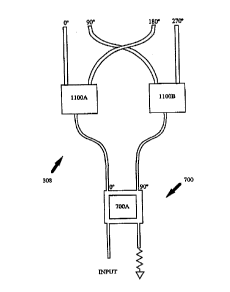
A first embodiment of feed circuit 308 combines two single-section
branch line couplers 700 and one 180 power divider 1100. This
embodiment is illustrated in FIG. 14. According to this embodiment, an
input signal is provided to the feed network at a point C. 180 power divider
1100 splits the input signal into two signals that differ in phase by 180.
These are referred to as a 0 signal and a 180 signal. Each of these signals is 35 fed into a single-section branch line coupler 700. Spe~-ific~lly, the 0 signal is
fed into branch line coupler 700A, and the 180 signal into branch line
coupler 700B.
SU~S I I l ~JTE SHEET (RULE 26)
CA 02202128 1997-04-OX
WO 97/06579 PCT/US96/13019
Branch line couplers 700A, 700B each provide two outputs that are of
equal amplitude but that differ in phase by 90. These are referred to as a 0
signal and a 90 signal. Because the input to branch line coupler 700A differs
from the input to branch line coupler 700B by 180, the 0 and 90 output
signals from branch line coupler 700A differ from the 0 and 90 output
signals from branch line coupler 700B by 180. As a result, at the output of
the feed network are the 0, 90, 180 and 270 signals required to feed the
quadrifilar antenna. Each of these 0, 90, 180 and 270 signals is fed to
radiators 104A, 104B, 104C, and 104D, respectively.
Another embodiment of feed circuit 308, illustrated in FIG. 15 uses
two 180 power dividers 1100 and one single-section branch line coupler 700.
According to this embodiment, single-section branch line coupler 700 first
splits the input signal to form two output signals of equivalent amplitude
that differ from each other by 90. These 0 and 90 degree output signals are
fed into 180 power divider 1100A and 180 power divider 1100B,
respectively. Because each 180 power divider 1100 produces two outputs
that are of equal amplitude but that differ in phase by 180, the outputs of thetwo 180 power dividers 1100 are the 0, 90, 180 and 270 signals.
Note, however, that these signals are not in the correct order. 180
power divider 1100A provides the 0 and 180 signals, while 180 power
divider 1100B provides the 90 and 270 signals. Thus, to provide the signals
to radiators 104 in the correct order, the 90 and 180 conductive paths must
change relative positions.
One way to change the relative position of the signals is to feed one of
these two signals to bottom surface 200 until it passes across the other signal.At this position the signal trace is etched as a patch on bottom surface ~00.
Around the patch is a clearing where there is no ground plane. This
clearing, however, has a negative impact on the ground. Therefore, it is
desirable to leave the ground as a continuous plane without any clearing
whatsoever.
In an alternative embodiment, the signal positions are exchanged by
running one conductive path across the other conductive path with an
insulating bridge between the two conductive paths. This allows the ground
plane to be continuous. In yet another alternative embodiment, the crossing
is made by running the signal trace across the ground plane using an
insulating section between the crossing signal and the ground plane. In this
alternative, the only interruption is for the vias allowing the signal to pass
through the ground plane on bottom surface 200.
SUBSTITUTE SHEET (RULE 26)
CA 02202128 1997-04-08
WO 97/06579 PCT~US96J~3~19
13
Although feed circuit 308 is described herein in terms of a quadrifilar
helix antenna requiring 0, 90, 180 and 270 signals, after reading the above
description, it will be apparent to a person skilled in the art how to
implement the disclosed techniques with other antenna configurations
requiring 0, 90, 180 and 270 signals. Furthermore, it will become
apparent to a person skilled in the art how to use 180 power divider 1100 in
other environments requiring two signals that differ in phase by 180.
It should be noted that the layout diagrams provided herein are
provided to illustrate the functionality of the components, and not
10 necP~s~rily to depict an optimum layout. Based on the disclosure provided
herein, including that provided by the illustrations, optimum layouts are
obtainable using standard layout optimization techniques, considering
materials, power, space, and size constraints. However, example layouts are
described below for branch line coupler 700 and 180 power divider 1100.
FIG. 16 is a layout diagram illustrating a layout for the feed network
illustrated in FIG. 15. Referring now to FIG.16, branch line coupler 700 is
shown in a layout that is more area efficient than the configuration
illustrated in FIG. 7. 180 power dividers 1100 are illustrated as having large
traces at interface areas to increase the capacitance and decrease the
characteristic impedance. Also illustrated in FIG. 16 is a cross-over section
1604 where the 90 and 180 si~nAl~ are crossed. Solid outlines without
hashing 162Z illustrate an outline of the traces on bottom surface 200. The
hashed areas indicate the traces on top surface 300.
FIG. 17(a) is an expanded view of cross-over section 1604. Note that a
conductive bridge to connect path A1 to path A2 is not illustrated in
FIG. 17(a). As illustrated in FIGS. 16 and 17(a), the conductive signal paths
exchange relative positions. The signal on conductive path A1 bridges over
conductive path B1 to conductive path A2. FIG. 17(b) illustrates the
conductive bridge A3 used to electrically connect (bridge) conductive path
A1 to conductive path A2. In the embodiment illustrated in FIG. 17(b),
conductive bridge A3 is implemented as a conductor 1740 mounted on an
insulating material 1742. In the embodiment illustrated, conductive tape
1744 or other conductive means, such as but not limited to solder or wires,
are used to ~lectri~ Ally connect conductor 1740 to conductive paths A1, A2.
35 In one alternative embodiment, conductor A3 is longer than insulating
material 1742 and ~lPctrit ~lly co~necterl to paths A1, A2.
FIGS. 18 and 19 illustrate the traces on the top and bottom sllrfa( ~s of
the microstrip substrate. FIG. 18 illustrates an exemplary layout for
SUBSTITUTE SHEET (RULE 26)
CA 02202128 1997-04-08
W 097/06579 PCT~US96/13019
14
conductive paths 1108 and 1110. Also illustrated is an area 1804 where via
1116 is located to connect to tab 1142. FIG. 19 illustrates ground plane 1112,
return conductive path 1109 and tab 1142.
FIG. 20 illustrates an exemplary layout of a quadrifilar helix antenna
5 using the feed network 308 illustrated in FIG. 16. Note that in this
embodiment, radiators 104 are shorted at second end 234 by signal trace 2004.
Note that, it will be apparent to a person skilled in the relevant art
after reading this document that although the various ground planes are
illustrated solid ground planes, other ground configurations may be utilized
10 depending on the feed network and/or antenna implemented. Other
ground configurations can include, for example, ground meshes, perforated
ground planes and the like.
6. Conclusion
The previous description of the ~re~l-ed embodiments is provided to
enable any person skilled in the art to make or use the present invention.
The various modifications to these embodiments will be readily apparent to
those skilled in the art, and the generic principles defined herein may be
20 applied to other embodiments without the use of the inventive faculty.
Thus, the present invention is not intended to be limited to the
embodiments shown herein but is to be accorded the widest scope consistent
with the principles and novel features disclosed herein.
What we claim is:
SU.,~ 111 UTE SHEET (RULE 26)