Note: Descriptions are shown in the official language in which they were submitted.
CA 02202198 1997-04-09
The present invention r¢lates to allenldtillg current (AC) transient voltage
surge suppression (TVSS) and electrical noise attenllation (being referred to hereinafter
as "TVSS filtering") incorporated into electrical distribution equipment, electrical power
protection devices or within the equipment to be protected.
BACKGROUNP OF TH~ INVENTION
TVSS f~ters have been available for decades and are not only stand alone
power protection devices but are often incorporated into other power protection devices
such as voltage regulators and unin~ ~lable power supplies. The Tn~titllte of Electrical
and Electronic Engineers (IEEE) has published numerous studies that indicate transients
(also called spikes or surges) and noise (also called high frequency low m:~gnit~ P
interference) related problems are the most frequent power disturbance problems. These
power disturbances have become more ~ignific~nt as microprocessor use has rapidly
expanded. Microprocessors are also becoming more susceptible to transients and noise,
causing equipment damage, logic control errors and expensive downtime.
There are many types of TVSS filter solutions. The basic circuit components
consist of some combination of the following:
1. Clipping Devices, which are activated by voltage above a certain
level and react to voltage only above the level. Typical components
include:
metal oxide varistor (MOV)
diode or transorb or avalanche diode or zener diode
CA 02202198 1997-04-09
2. Crowbar devices, which are activated by voltage above certain levels
and short the power line until the incoming voltage is lowered to a
pre-determined level. Typical components include:
spark gap
gas tubes
thyristor (SCR)
3. Electrical noise filter components, which are energy storage devices
that react to frequency changes. Typical components include:
AC capacitors
inductors or chokes or coils
These components can be arranged in a infinite number of circuits creating
effective TVSS and TVSS filters. ~any circuits have been used for a number of years
and a large body of prior art exists such as prior products, electrical engineering teachings
and electrical association recommendations.
Patents for TVSS filter circuits include: U.S. Patent Nos. 4,912,589;
4,628,394; 4,563,720; 4,068,279; 3,793,535 and C~n~ n Patent No. 1,332,074.
There are many locations where TVSS f~ter circuits can be applied within
a facility. The most common location uses a TVSS device between a wall receptacle and
the load to be protected. Another location is within the application or load itself, although
the circuits utilized at this location often just contain MOVs. A third location is for a
TVSS filter circuit to be attached or designed within the electrical distribution equipment
of a facility. This equipment includes circuit breakers, meter panels, panel boards, switch
boards, switch gear and motor control centres. The invention can be located in any of the
CA 02202198 1997-04-09
above locations but is most economical when applied in the electrical distribution
equipment.
Prior art electrical power protection circuits have dramatically improved with
the use of clipping components (especially MOVs) and AC capacitors. MOVs are able
to repeatably shunt large transients and are activated by voltage above a certain level.
Their limitation is the voltage level at which the MOV begins to react. For a 120 VAC
system the nominal peak voltage is 172 VDC. The system VAC can be as high as 127VAC with a peak voltage of 180 VDC Hence the MOV cannot begin operations below
180 VDC, at it would quickly deteriorate. The level at which the MOV begins operation
is called the maximum continuous operating voltage (MCOV) and the lower it is set, the
lower the let through voltage. Let through voltage is the rem~ining voltage of a transient
after being reduced by a power protection device. The problem with setting a lower
MCOV for MOVs is that it can dramatically reduce the life of the MOV. To maximize
lifetime, 200 % or greater MCOV compared to peak voltage (VAC peak = 1.414 x Vrms)
has a very long life and survives the possible problem of continuous over voltage caused
by mis-wiring within the electrical system.
Below 115 % of peak voltage, a clipping device is very susceptible to utility
surges and transients which subst~nti~lly shorten the component' s life. At 115 % to 200 %
a clipping device can be damaged by continuous over voltage and extreme surges while
having a reasonable life in a standard environment.
AC capacitors react to voltage frequency changes and hence absorb high
frequency electrical noise and small transients. AC capacitors however, release energy
back relatively slowly to the system allowing them to be overwhelmed by continuous and
CA 02202198 1997-04-09
severe high frequency electrical noise and harmonics. For higher voltages such as 208,
480, and 600 volt systems, the size and cost of effective AC capacitors can become
prohibitive.
The combined use of MOVs and AC capacitors provides a range of
protection, from small transients and high frequency electrical noise, to large surges. The
combined use also provides current sharing where each component absorbs or shunts a
portion of a transient's energy which extends the life of all components. This current
sharing is limited by the cost and size constraints of AC capacitors and the MCOV of
MOVs. What is required, however, and what the present invention intends to provide,
is a component or circuit that can be set near to the peak voltage level to be encountered
from the utility and absorb or shunt transients ranging to above 200 % of this peak voltage.
This would allow much better sizing of AC capacitors as the effect of current sharing,
from this invention, would help protect them from continuous electrical noise and
harmonics. MOVs could also be set at a higher MCOV, dr~m~tic~lly increasing their life.
Many dirrt;~ l arrangements using clipping, crowbar and electrical noise
f~ter devices have been proposed to achieve greater durability and lower the let through
voltage. The general result has been greater current sharing through a greater number of
components. The present invention has taken a very dirrel~lll approach of using direct
current (DC) components within a circuit that achieves low MCOV, long life, and robust
current sharing in the 100% to 200% range of peak voltage. When combined with
clipping devices and AC capacitors, the total of all devices provides much lower let
through voltage and greater durability.
The invention is similar to an AC to DC power supply used in many typical
CA 02202198 1997-04-09
electrical and electronic products. The foremost common power supply circuits are the
half-way rectifier (HWR) which is able to handle either positive or negative surges, but
not both, the full-wave center tap (FWCI~, the dual complimentary rectifier (DCR), these
latter two both requiring a center tap transformer while the DCR also requires grounding,
significantly reducing the configurations these latter two circuits can be applied to for
power protection purposes, and the full-wave bridge (FWB). When altered for power
protection, the FWB is able to handle both positive and negative electrical disturbances
and work on all electrical col~lgurations. To be utilized for power protection however,
such circuits would need to be subst~nti~lly altered.
While the inventor is not aware of any commercial use of an adaption of the
FWB for power protection, three existing patents are known which teach the use of
diodes.
U.S. Patent No. 4,321,644 issued March 23, 1982 does not relate to the
invention but the prior art in the patent does. This prior art applies diodes but in a very
complex manner with non-disclosed trigger signal devices controlling the diodes. The
capacitor appears to be an AC capacitor. The use of an AC capacitor within the circuit
would have a zero charge causing a large initial current draw, high recovery time, and
rebound effects. The invention has none of these restrictions or the complexity of the
circuit.
C~n~ n PatentNo. 1,230,919datedDecember29, 1987usesDCcapacitors
but has no resistor and uses Zener diodes. The circuit is designed as a cascade where the
DC capacitors handle smaller surges while the Zener diodes activate for large surges. The
circuits send transients to ground, unlike the invention, which absorbs transients and then
CA 02202198 1997-04-09
dissipates the energy by utili~ing a resistor.
U.S. Patent Nos. 4,870,528 and 4,870,534 dated September 26, 1989 are
replicated in C~n~ n Patents Nos. 1,332,439 and 1,333,191. We will only deal with
U.S. Patent No. 4,870,534 as it is more generic in nature while U.S. Patent No.
4,870,528 is a three wire detailed adaptation of U.S. Patent No. 4,870,534. The patent
utilizes the invention circuit for power protection use in a much different manner. Rather
than combine the circuit in parallel with MOVs or AC capacitors, the patent goes to
lengths to discredit these components for power protection use. Instead the patent relies
on a two tiered approach with each tier co.l~ ing a coil or inductor and then the adoption
of the FWB circuit. These two patents limit the circuit's use to series circuits of only one
phase. The invention, in~te~d, uti1izes parallel circuits with clipping devices (MOVs,
Avalanche diodes, Zener diodes) and/or AC capacitors. This dramatically expands the
operating amperage range the invention can be uti1ized for. Series products meanwhile
must be accurately sized for their application. Multiple phases with ground and/or neutral
configurations can also be uti1ized with the invention. The LED indicator in the circuit
is also not included in the invention's circuit. The parallel nature of the invention circuit
allows a signal to be monitored at a sensor board on the device, if monitoring is required.
OBJECTS OF THE INVENTION
The objects of the invention are:
- improved power protection performance typically measured as lower
let through voltage;
CA 02202198 1997-04-09
- greater durability and longer life for the invention and protected
equipment;
- lower cost;
- smaller size; and
- simplicity to m~nllf~( ture.
SUMMARY OY THE INVENTION
The invention is a combination of an altered AC to DC circuit utilized with
typical power protection components for improved power protection purposes.
More particularly, in accordance with the present invention there is provided
a parallel circuit to protect electrical and electronic equipment from transients from an
electrical system. The circuit comprises (a) first uni-directional diodes directly attached
to line, neutral and/or ground connection of the electrical system; (b) a DC capacitor with
a positive pole being fed by said first uni-directional diodes; (c) uni-directional diodes
directly attached and feeding back to line, neutral and/or ground connection, and being
lS fed from a negative pole of the DC capacitor; and (d) a discharge resistor in parallel with
said DC capacitor.
The circuit according to the present invention is combined in parallel with
clipping devices and/or AC capacitors and/or over current protection, as will be described
in more detail hereinafter, to provide the desired protection from transients.
More particularly, the adapted AC to DC circuit consists of:
1. Diodes which convert AC to DC power and trigger levels set as low
CA 02202198 1997-04-09
as 0.7 volts above the peak AC voltage. When a surge or over
voltage exceed this trigger level, the diode converts the energy above
this level to DC voltage. As the diodes are in a FWB circuit either
positive or negative surges will be converted.
2. DC capacitor which absorbs the positive DC electricity converted by
the diodes and stores the excess energy. DC capacitors are a much
smaller size and have a lower cost compared to comparable AC
capacitors, allowing for much greater energy storage. The capacitor,
once charged above its trigger level, will discharge the stored energy
as positive DC electricity, which must flow through the resistor, as
the diodes are uni-directional.
3. The resistor dissipates the DC power which is discharged by the DC
capacitor. No electrical energy is released back to the system.
Proper sizing of resistors allows for controlled dissipation of energy
to the typical charged state of the capacitor which is just above the
peak system voltage.
The above circuit is called a DESD circuit (diode to energy storage to
dissipation). This new circuit must be included with other power protection components
to provide subst~nti~lly greater performance and durability over other described power
20 protection circuits.
The DESD is to be wired in parallel with the other components of the power
protection circuit. These components must consist of clipping devices either before and/or
after the DESD and over current devices between the live lines and the rest of the power
CA 02202198 1997-04-09
protection circuit. AC capacitors are optional to provide attenuation of electrical noise.
They can be ~it~ tcd either before and/or after the DESD. The power protection circuit
is wired in parallel with the electrical system it is protecting.
The DESD circuit has been described an alteration to a FWB which uti1izes
only a single phase and neutral or ground. The DESD can in fact be altered to handle up
to 3 phase and neutral, ground, or both. Two additional diodes for each added phase,
neutral or grounded are required.
BRIEF DESCRIPIION OF THE DRAWINGS
These and other advantages of the invention will become ap~al~ -l upon
reading the following detailed description and upon l~rellillg to the drawings in which:-
FIGURE 1 is a single line schematic of a typical prior art single phase,
wye, TVSS filter wired in parallel;
FIGURE 2 is a single line schematic of a typical prior art single phase,
wye, TVSS filter wired in series;
FIGURE 3 is a single line schematic of the invention for a single phase,
with the DESD circuit not fully detailed;
FIGURE 4 is a single line schematic of the DESD circuit for a single phase;
FIGURE 5 is a single line schematic of the DESD circuit where all modes
are protected for a three phase, wye;
FIGURE 6 is a single line schematic of three separate DESD circuits that
protect line to neutral modes for a three phase, wye;
CA 02202198 1997-04-09
- 10 -
FIGURE 7 is a single line schematic of four separate DESD circuits that
protect all modes for a three phase, wye;
FIGURE 8 is a single Line schematic of .llini..-~ types of power protection
components to be utilized with the DESD circuit(s) for a three phase wye
system; and
FIGURE 9 is a single line schematic of the maximum types of power
protection components to be utilized with the DESD circuit(s) for a three
phase wye system.
While the invention will be described in conjunction with example
embodiments, it will be understood that it is not intended to limit the invention to such
embodiments. On the contrary, it is intended to cover all alternatives, modifications and
equivalents as may be included within the spirit and scope of the invention as defined by
the appended claims.
DETAILED DESCRIPTION OF THE INVENTION
FIGURE 1 details a conventional single phase wye power protection circuit
10 that provides both TVSS and f~tering. The TVSS is provided by clipping devices 1 la
and 1 lb. 1 la are MOVs and 1 lb are avalanche diodes. Both are wired in parallel across
each mode. The filter is provided by AC capacitors 12, again wired in parallel across
each mode. The f~ter is provided by AC capacitors 12, again wired in parallel across
each mode. Over current protection if a component at 10 fails short, is provided by a
circuit breaker 13a.
CA 02202198 1997-04-09
To increase performance, clipping and crowbar components with lower let
through voltage can be used. However these types have low MCOV that shorten life and
reliability. AC capacitors are able to absorb much of the energy between peak system
voltage and the trigger voltage level for small surges but has minimum effect for large
surges without sacrificing reasonably cost and size. Thus the combinations of clipping
components and AC capacitors are limited to either higher let through or much shorter life
and reliability.
For example, a system with one 20 mm MOV would have the following
results based on mAmlfA(~lrer's let through results and expected life using ANSI/IEEE
C62.41 surge probability medium exposure level.
EXAMPLE 1
l\IVOC Let Throll~h EYpected Life
130 340 VDC 12.1 years
150 395 VDC 13.2 years
250 650 VDC 20.5 years
FIGURE 2 illustrates a conventional series filter utili7ing clipping devices
21a and 21b, AC capacitor 22, fusing 23b and inductors 24. The use of inductors is for
filtering and is used only on series filters. Series filters' greater performance is limited
by si7ing restrictions as a series filter's components must be sized to the typical amperage
and voltage of the system. The invention does not relate to series power protection
CA 02202198 1997-04-09
circuits.
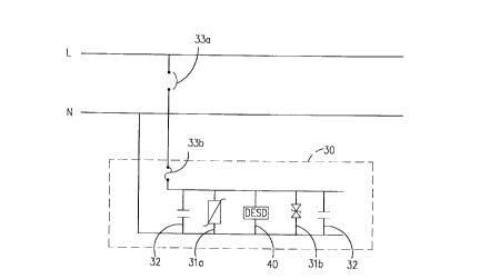
FIGURE 3 outlines possible components to be used in conjunction with the
present invention. The DESD circuit 40 of the present invention, detailed later, is wired
in parallel across the power protection circuit 30 which is wired in parallel to the electrical
S system it is protecting. All other components are wired in parallel within the power
protection circuit except over current protection on the line wire, which can be either
fusing 33b, circuit breaker 33a, or both. To provide TVSS protection, the DESD 40
absorbs some of the surge with clipping device 31a and 31b, which are MOVs and zener
diodes, ~hllnting the remainder. AC capacitors 32 are optional to provide electrical high
frequency noise attenuation, also called filtering. Their use also provides some current
sharing for larger surges causing less stress on other components and lower let through
voltage to the protected load. The use of the DESD circuit enhances the performance of
AC capacitors as its trigger point is just above the system's peak voltage, allowing current
sharing for smaller spikes and electrical high frequency noise.
FIGURE 4 is a schematic of a simple DESD circuit 40 protecting one mode
of line to neutral. A positive surge on the line wire of above the peak voltage would
trigger the diode 45a flowing from the line wire. The diode would convert the surge to
DC electricity which is then absorbed by the DC capacitor 46. The DC capacitor then
releases the stored energy in a controlled, steady manner as positive DC power. This
power must flow through the resistor 47, as the circuit will only allow the DC power to
flow in that direction as diodes 45a are uni-directional. The resistor 47 ~ ip~tes the
energy in a controlled manner. The DC capacitor returns to a charged state of peak
system voltage within seconds. The circuit is bi-directional, or able to handle surges in
CA 02202198 1997-04-09
- 13 -
either direction, as a surge on a neutral would be converted to DC electricity by diode 45a
connected to the neutral line. Diodes 45b complete the circuit.
FIGURE S provides another version of the DESD circuit 50. Rather than
protecting a single mode as in FIGURE 4, this version protects 10 modes (3 L-L, 3L-N,
3L-G, lN-G) which are all combinations of a 3 phase, wye system. While the DC
capacitor and resistor sizing would change, their basic circuit function would remain the
same as in DESD circuit 40. However, five incoming and five outgoing diodes would be
used or one incoming and one outgoing per line, neutral, or ground. As in DESD circuit
40 the incoming diodes are to the positive side of the DC capacitor and the outgoing
diodes are from the negative side of the DC capacitor.
One drawback with all modes being protected by a lone DESD circuit is that
the DESD trigger point is increased. In FIGURE 4, if the line voltage was 120 VAC, the
peak system voltage would be 170 VDC and the DESD's trigger voltage would be setslightly in excess of 170 VDC. For FIGURE 5, if each line's voltage was 120 VAC, the
three phase system voltage would be 208 VAC and the peak operating voltage would be
294 VDC. Thus, the DESD trigger voltage would be slightly in excess of 294 VDC
causing the DESD circuit 50 to be less effective than DESD circuit 40.
FIGURE 6 provides a version of the DESD circuit that solves the drawback
of DESD version 50. Basically, a simple DESD circuit 40 is provided for each mode that
requires added protection. In circuit 60, only three line to neutral modes are protected.
This provides the lower trigger point per mode achieving better pe rollllance, although at
a higher cost and size. This single DESD circuit per mode could be applied to all ten
modes requiring ten DESD circuit 40's. The L-N and L-G trigger points for a 120/208
CA 02202198 1997-04-09
- 14 -
three phase system would be at 170 V~)C. If circuit 40 was applied to other modes, their
trigger points would be 295 VDC (208 VAC) for L-L and 1 VDC for neutral to ground.
FIGURE 7 is an example of the combinations between DESD circuits 40 and
50 to create a circuit 70 that provides both performance and cost effectiveness. DESD
circuit 40 is utilized for two of the three line to neutrals with the third line to neutral
including ground. This protects neutral to ground at a trigger point of 170 VDC for a
120/208 three phase system. Line to ground is protected under a DESD circuit that
combines the three lines and ground. The trigger point for these modes is 295 VDC.
Hence all modes are protected with four DESD circuits, which saves on cost and size, but
protects certain modes to a greater degree as their trigger points are lowered.
FIGURE 8 provides an overview of the minimum combination of types of
components with the DESD circuit(s) which, when combined, provide a TVSS power
protection circuit. The DESD circuit(s) must be included and can be as in 50, 60, 70, or
some other combination within a circuit 80. Not all modes need to protected with DESD,
although for maximum protection, this is advisable.
Clipping devices 81, such as MOVs, avalanche diodes (also called transorbs
and zener diodes) must be included and be wired in parallel. Not all modes need to be
protected, although for maximum protection, this is advisable.
The clipping and DESD circuit components must be separated from the
parallel connection to the rest of the system by some type of over current device on the
line wire. FIGURE 8 this is achieved by fusing components 83.
FIGURE 9 provides a more elaborate version of the invention as circuit 90.
Two DESD circuit(s) of 50, 60, or 70 blocks are provided although the duplication is
CA 02202198 1997-04-09
- 15 -
unlikely to improve performance significantly. Dual clipping component blocks 91improve performance, durability, and life because of current sharing. Within a mode,
multiple clipping or AC capacitor components, all parallel with each other, may exist.
This provides further pelrol-nance and durability of components. If a component fails
short, fusing components will open. If a component fails and remains open, duplicate
components can continue to operate. AC capacitors provide f~tering and two blocks of
AC capacitors (92) will improve performance and durability.
The entire circuit is separated from the parallel connection to the electrical
system by over current protection on the line wires. Fusing 93b is included within the
power protection circuit 90 while the circuit is wired into circuit breaker 93a for added
protection. In some circumstances circuit breakers 93a may suffice.
The above explanation and figures explain the use of the DESD circuit within
parallel connected power protection circuits utili7ing fusing, clipping devices, and AC
capacitors. For three phase electrical systems, while the above explanation and figures
describe a 120/208 system use of the DESD circuit in accordance with the invention, it
is also envisaged that this invention extends to other typical three phase systems such as
a 277/480 system, (in which case the L-N trigger point would be at slightly in excess of
392 VDC and L-L at slightly in excess of 679 VDC) and a 347/600 system (in which case
the L-N trigger point would be at slightly in excess of 490 VDC and L-L at slightly in
excess of 848 VDC). The advantages of the DESD circuit become appa~ when
comparing the use of this circuit to other power protection components. The DESDcircuit has the following advantages:
1. Clipping and crowbar devices with low trigger points which reduce
CA 02202198 1997-04-09
- 16 -
the let through voltages, havc low MCOV which shortens their life,
and reliability. The Dl~SD circuit has a trigger point at
approximately the peak voltage of the power system which
subst~nti~lly reduces let through voltage. The DC components within
the DESD circuit are not prone to deterioration for low MCOV
which subst~nti~lly extends its life and increases reliability.
2. Where mis-wiring or other causes creates extended over voltage
which is above the trigger point of clipping devices, these devices
will quickly fail. In similar circumstances, the DESD reaches a
charge on the DC capacitor which it would then hold. No long term
damage would result to the DESD circuit. This robustness of the
DESD circuit allows clipping devices to have higher trigger points
within the power protection circuit. For example, on a three phase
system, two phases incorrectly combined create 208 VAC. With the
lS invention, clipping device trigger points can be set above this level
with the assurance that performance is not lost due to the DESD.
3. AC capacitors have higher costs and prohibitive sizes than have the
DC components used in the DESD especially at higher voltages and
~;u-le~ . Thus the DESD allows smaller and more economical DC
capacitors to be used as the DESD circuit is able to handle much of
the energy AC capacitors once handled between 100% to 200% of
peak system voltage.
4. Harmonic resonance requires AC capacitor and inductor components
CA 02202l98 l997-04-09
- 17 -
to carry much greater CU~ under normal operations and during
power disturbances. This subst~nti~l1y reduces the life of the AC
power protection components. The DESD is immune to harmonics
as all its components are PC components which are immune to
harmonics.
5. Crowbar devices are inherently slower and have, in comparison, a
very high clamp voltage. Puring operation they will short out the
power line. The DESD circuit has a very low trigger voltage at
approximately peak system voltage and will not reduce or short the
system voltage.
6. The DESD has much higher energy storage than AC capacitors at
similar cost or size.
7. Energy from the DESD is not released back into the system.
8. DESD provides the majority of current sharing in the most vulnerable
range of power disturbances for clipping and AC capacitor
components. This range is between 100% and 200% of peak system
voltage.
9. For prolonged over voltage above the DESD circuit trigger point the
DESD is not damaged where clipping devices are quickly destroyed
when exposed to prolonged over voltage above their trigger point.
Thus, it is apparent that there has been provided in accordance with the
invention an improved transient voltage surge suppression and electrical noise attenuation
circuit that fully satisfies the objects, aims and advantages set forth above. While the
CA 02202198 1997-04-09
- 18 -
invention has been described in conjunction with example embodiments thereof, it is
evident that many alternatives, modifications and variations will be apparent to those
skilled in the art in light of the foregoing description. Accordingly, it is intended to
embrace all such alternatives, modifications and variations as fall within the spirit and
S broad scope of the invention.