Note: Descriptions are shown in the official language in which they were submitted.
CA 02202~30 1997-04-11
W~96113051 PCT~S94113758
INDUCTIVELY CCUPLED PLASMA SPUTTER CHAMBER WITH
CONDUCTIVE MATERIAL S~Ul~ING CAPABILITIES
Field cf the Invention
The present invention relates to
inductively coupled sputtering o~ conductive
materials.
Backqround of the Invention
In a sputtering process, a substrate to be
,. . .
processed, such as a semiconductor wafer, is mounted
in a vacuum chamber reactor filled with a gas. The
gas in the reactor is subjected to electrical
excitation, producing a plasma in the reactor. In a
sputter etching process, ions from the plasma
bombard the surface of the substrate, ejecting
particles of any coating on the wafer surface. The
ejected particles predominantly adhere to and coat
the interior surfaces of the reactor. In a sputter
coating process, a target is placed in the reactor,
CA 02202530 l997-04-ll
and ions from the plasma ~ombard the target,
ejecting particles from the target which adhere to
the wafer and the interior surfaces of the reactor.
In an inductively coupled sputtering
~S v~, ~/ ~co~_p~ ~P~ ~1491L~o~L;,'2"
reactor,Lthe chamber is nonconducting. Electrical
excitation is in part provided by magnetic fields
generated by a helical coil formed around the
outside of the chamber. The coil is separated from
the chamber by a magnetically impermeable barrier
wall such as a quartz jar.
A difficulty with inductively coupled
sputtering of metals or other electrically
conductive coatings is that particles sputtered,
e.q., from the warer, tend to form a conductive film
on the inside of the chamber. If the chamber is not
cleaned reqularly, this film will accumulate, and
the resistance of the film will be small enough that
magnetic fields from the coil will induce eddy
currents in the conductive film. These eddy
currents will tend to oppose penetration of magnetic
fields from the coil into the chamber, deterioratlng
plasma ignition performance, or in severe cases
preventing plasma ignition altogether.
Regular cleaning or replacement of the
chamber can be costly both in effort expended and in
B S~FJ
CA 02202530 1997-04-11
WO 96/13051 PCT/US94/13758
downtime. And, even regular cleaning does not
prevent some performance reduction as conductive
films acc~ llate inside the reactor. Accordingly,
significant cost and performance advantages can be
gained from an inductively coupled plasma sputter
etching reactor which is not susceptible to plasma
deterioration due to conductive film accumulation on
the interior of the reactor ch~h~r.
SummarY of the Invention
In accordance with principles of the
present invention, a shade is disposed on the inside
wall of an inductively coupled plasma chamber. The
shade covers a protected zone of the wall generally
opposite to the inductive coil driving the ch~h~r,
and prevents accumulation of sputtered material in
this zone, thus reducing closed paths for eddy
current flow along the chamber wall, and improving
inductive coupling of electrical power to the plasma
in the chamber.
In specific ~ho~ i ments, the shade is
elongated and has its elongated direction generally
parallel to the axis of the inductive coil. The
shade includes one or more SU~Ol Ls in contact with
the chamber wall and ext~n~;ng generally inwardly
from the chamber wall, supporting an elongated hood
CA 02202~30 1997-04-11
WO96/13051 PCT~S94/13758
which extends generally tangentially (parallel to
the chamber wall) from the support, covering the
protected zone. In some ~hoAi~ents, two or more
elongated 5h~ may cooperate to cover the
protected zone.
The shade may cover a protected zone
ext~n~ing across the entire length of the coil; or,
alternatively, the shade may cover only a partial
length of the coil, so long as eddy current paths on
the inside of the reactor are sufficiently inhibited
to allow inductive coupling of power from the coil
to a plasma in the chamber.
A chamber in accordance with the invention
is thus not susceptible to eddy currents caused by
accumulation of a conductive film on the inside of
the chamber, thus improving plasma ignition
performance, and reducing the need for costly
regular cleaning of the chamber. These and other
objects and advantages of the present invention
shall be made apparent from the accompanying
drawings and the description thereof.
Brief DescriPtion of the Drawinq
The accompanying drawings, which are
incorporated in and constitute a part of this
specification, illustrate ~hoA i~ts of the
.
CA 02202~30 1997-04-11
WO96/13051 PCT~S94/13758
invention and, together with the general description
of the invention given above, and the detailed
description of the embodiments given below, serve to
explain the principles of the invention.
Fig. 1 is a cross-sectional view of an
inductively coupled plasma processing reactor;
Fig. 2A is a cross-sectional view of the
reactor of Fig. 1 fitted with a conductive cylinder
simulating the effect of accllrtllAtion of a
conductive film in the ~hA h~7-;
Fig. 2B is a plan view of the reactor of
Fig. 2A taken along line 2B-2B;
Fig. 3A is a cross-sectional view of the
reactor of Fig. 1 supplied with a bench shaped shade
22 which prevents ac~l~lllAtion of conductive film in
a protected zone 24 along an elongated section of
the chamber wall;
Fig. 3B is a plan view of the reactor of -
Fig. 3A taken along line 3B-3B, and Fig. 3C is a
perspective view of the shade 22;
Figs. 4 and 5 are diagrammatic partial
plan views of alternative embodiments of a shade
preventing ac~ 71Ation of conductive film in
protected zones 24' and 24".
- 5 -
CA 02202530 lss7-04-ll
Detailed DescriPtion of SPecifiC Embodiments
Referring to Fisure 1, an inductively
coupled plasma reactor lO, for example a plasma
sputter etching reactor, has in general a helic~1 or
spiral coil 11 for plasma excitation which is wou~d
around a cylindrical chamber lZ, for example a
;~3 G ~5 C_
quart2 jar having a~(12 inchJ diameter, height of;
~ 3c_
approximatelyL(8 inches)and wall thickness o~
approximatelyl(one-quarter inch). Jar 12 must
L 1 3~o~~sl~
withstand high vacuum, for example ofL(10~ Torr). The
coil 11 and jar 12 are supported by a housing
platform 16 and contained within a housing (not
shown).
I~-2~
Coil 11 is manufactured of aL(50 foot)
3 ~
length ofl(one-ei~hth inch)diameter copper tubin~,
wound into approximately 15.5 turns around the outer
surface of jar 12. Electrical terminals are
connected to the ends of the copper tubing. Cooling
water flows through the center of the tubing to
stabilize the coil's operating temperature.
Coil 11 is electrically excited at a
medium range frequency, such as in the range of lOO-
800 kHz, or specifically 450 kHz, to produce a
magnetic field inside of the jar 12. Electrical
excitation for coil 11 is qenerated by a power
AMENDED SH~R
CA 02202530 1997-04-11
supply (not shown), such as a PDP 2500 450 kHz 2000
Watt generator, available from Advanced Energies
Industries, Inc., 1600 Prospect Par~way, Fort
Ccllins, CO 84525. Approximately 1250 Watts of
electrical power are consumed ~y the coil. This
electrical ener~y is coupled to coil 11 through a
power matchinq networ~ (not shown), such as the
power matching networ~ for the RMX-10 and RMX-12,
available from Mater~als Research Corporation, Route
lo 303, Oranqeburg~ NY 10962. The electrical
connections and the frequency o~ excitation of the
coil 11 will differ for di~ferent specific
applications.
A wafer 13 to be processed in the plasma
sputter etching reac~or is placed on a wafer chuc~
14 inside of jar 12. Wa~er 13 may have a diameter
10 :~ h ao-3 c~
of~(four to eight inches), but in the illustrated
~ o 3 c~
process the wafer has anL(eight inch~diameter. Jar
12 is evacuated to near vacuum conditions by a
vacuum pump (not shown). Radio frequency (RF) power
is applied to the wafer chuck 14 relative to the
housing 15 and platform 16, e.g., at a frequency of
13.56 MHz and a power level of approximately 2000
Watts, generating a 125 Volt DC voltage on the wafer
durinq the process. One suitable power supply is a
~M~ID~ SltEE~
-
CA 02202530 l997-04-ll
model AEG-lOB-02 RF power generator, available from
ENI corporation, a division of Astec America, Inc.,
lOO Hiqh Power Road, Rochester, NY 14623. At the
same time, medillm ranqe frequency energy is applied
S to coil 11, as discussed above.
A ~as flows into the evacuated ~ar 12 at a
low rate, producin~ a low pressure. For example,
Argon flows into jar 12 at a rate o~ 15-50 sccm,
6~_,3~ x~o~3 ~l~2
e-q-, 20 scc3m,/at a pressure o~l(O.5-1 milliTorr),
e.g.,L(0.7 milliTorr~
The combination of electrical excitation
from coil 11 and from RF power applied to chuc~ 14
causes the gas in jar 12 to i^nize and foLm a ~as
plasma inside of ~ar 12. Ions from ths plasma
bombard the surface of wafer 13, causing any exposed
film on the surface of wafer to sputter away from
the surface 13 and into jar 12. Thus the surface of
the wafer is etched by plasma bombardment.
Processing of a wafer takes about 120 seconds.
As illustrated in Fig. 1, jar 12 includes
a reentry tube 15 havin~ a cylindrical section and a
1~ lc~
diameter of approximately~four and three-quarter
inches). Reentry tube 15 extends from the surface of
~ar 12 to a closed end 17 spaced approximately
l q c,_
Z5 L(three-quarter inches) fro~ the sur~ace of the wafer.
- 8 -
P,N EN~E~ S~
CA 02202~30 1997-04-11
WO 96/130Sl PCT/US9'1/13758
The inside of this reentry tube is open to the
atmosphere outside of jar 12, i.e., is not
evacuated. Reentry tube 15 prevents formation of a
plasma in the central section of jar 12, and thus
re~-lc~ the etching rate at the center of the wafer.
Without the reentry tube, the etchi~q rate on the
wafer would be significantly higher at the center of
the wafer than at the edges. The reentry tube
reduces the etching rate at the center of the wafer,
resulting in more uniform etching of the wafer.
During the etching process materials
removed from the wafer are predo~in~ntly deposited
on the inner surface of the jar 12. Etc~;n~ of
metals or other conductive materials from the
surface of wafer 13 causes a conductive film to form
on the interior surface of jar 12. The conductivity
of this layer grows with the number of wafers
processed in the jar 12. Etching of some non-
conductive metal-cont~;ning films may have similar
consequences due to chemical reactions which occur
during processing.
A conductive coating formed on the
interior surface of jar 12 behaves as an electrical
shield which prevents coil 11 from coupling magnetic
field into the process gas in jar 12 and therefore
CA 02202530 1997-04-11
preventing plasma ignition. Chanqing magnetic
fields produced by coil 11 induce eddy currents in
the conductive coating. The eddy currents will
circulate in the conductive film around the
cylindrical walls of jar 12 in the direction
generally parallel and opposite to the direction of
current flow in coil 11. The induced eddy currents
produce an equal and opposite maqnetic field in jar
12, tending to repel and eliminate magnetic flelds
generated ~y coil 11.
When a conductive film of sufficient
thic~ness has accumulated on the inside of ~ar 12,
it will ~ecome impossible to ignite a plasma inside
of the jar 12. As a result, ~ar 12 must be cleaned
or replaced for further processing to be per~ormed.
This can result in significant costs and down time
in the etching process.
Difficulties associated with deposition of
the conductive films on the inside of a plasma
processing chamber were demonstrated as follows.
I5 2c~
L(SiX inch)silicon wafers, covered with 100 nm
deposited titanium films, were etched using
inductively coupled plasma etching inside the
reactor shown in Fig. 1, under conditions discussed
above. After 20 to 25 wafers had been etched in
-- 10 --
AM'NDEB S~E~T
CA 02202530 lsg7-04-ll
this manner, plasma i~nition completely failed and
further processin~ was impossible. At this time,
the interior of jar lZ was examined and it was found
that a conductive film had deposited on the interior
of the jar havinq sheet resistance of between 30 and
400 ohm-meters in the area of coil 11, as measured
l a~ ~
with probes placed a distance ofL(cne-half inch)apart
on the interior surface of the jar. Lower values o~
sheet resistance were recorded at regions of the jar
at close proximity to the surface of wafer 13 from
which material ~as being sputtered.
In accordance with the principles of the
present invention, the above dif~iculties are
alleviated by preventing the creation o~ a
continuous path of deposited material on the
interior of jar lZ throu~h which eddy currents may
flow. This is done by creating a non-conductive
protected zone, having an elongated shape, on the
inner surface of the jar, placed in a direction
generally parallel to the central axis o~ jar 12 and
coil 11 and perpendicular to the direction of flow
of induced eddy currents. This non-conductive
protected zone prevents the flow c~ significant eddy
currents in a conductive film on the inside of
-- 11 --
,s
~ E~IDE~ SHEET
CA 02202530 lsg7-04-ll
quartz jar 12, thereby preventing generation of
opposing maqnetic fields.
Referring to Fiqs. ZA and 2B, the
feasibility of preventing eddy currents through the
S use of a protected zone was proven by fabricating a
stainless steel test element 18 for insertion inside
of jar 12. Test element 18 was manufactured of shim
stoc.~ stainless s~eel no. sS-304, which has a
a l53 ~ /5 3 c~
thic~ness ofl(0.00~ inches)and a width of~6.0 inches).
0 Thls shim stoc~ was bent into a cylindrical section
4 4~C~
havinq a gap Z0 ofL(1.75 inches) to form test element
18. This test elemen~ 18 was installed inside of
jar 12, to simulate the expected thickness o~ the
conductive layer accumulated on the inside o~ ~ar 12
after processing of ~ore than 3,000 wafers by
sputter etching. Test wafers having a thermal oxide
top layer (i.e., a non-conductive top layer) were
placed into the chamber, and RF and inductive power
were applied to the chamber to simulate plasma
processinq. (A non-conductive wafer was used to
insure that conductive material would n~t be
sputtered from the tsp layer o~ the wafer into gap
20, causing a short across gap 20.)
The test apparatus as described above
2S exhibited timely and sustained plasma ignition,
- 12 -
h!DC~ E~
CA 02202530 1997-04-11
apparent~y una~fected by the presence of stainless
shim stoc~test element 13 in the cham~er. This
performance confirmed that inclusion of a non-
conductive protected zone on the inside surface of
S iar 12 would prevent eddy current flow and would
eliminate difficulties arising from acc~mulation of
conductlve materials on the inside sur~ace of jar
12.
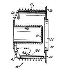
Referrins to Figs. 3A and 3~, one
embodiment of a shade ~or preventin~ accumulation of
conductive material on the inside wall of jar 12
within a protected zone taXes the ~orm o~ an bench
22. Bench 22 comprises, 2S shown in Fig. 3B, two
supports 21 which rest on the jar wall, and a hood
lS 23 ~hich extends in its elongated direction for
approximately the entire length of coil 11 in a
direction parallel to the axis o~ cail 11. Supports
21 and extends radially inward (toward the center of
o 3a ~ o q~c~
jar 12) approximately~one-eighth to three-eighths of
an inch~, and support hood 23 at this approximate
height from the wall o~ iar 12. Hood 23 extends in
a tangential direction approximatelyL(two inches),
creating a protected zone 24 which is shaded from
materials sputtered from wafers inside of jar 12.
Hood 23 and supports 21 are manufactured of quartz.
- 13 -
!D~
CA 02202530 1997-04-11
Due to the presence of hood 23, material
sputtered from a wafer, or from a taryet in a plasma
sputtering system, will not coat the area of ~ar 12
in the protected zone 24. As a result, although a
conductive coating will form over time on the inside
surfaces of jar 12, no conductive coating will form
in protected zone 24. Therefore eddy currents
cannot flow throu~h protected zone Z4, and thus
cannot flow in an even, circumferential pattern
around the cylindrical section of the interior of
jar 12.
Figure 4 illustrates an alternative
embodiment of a shade 26 suitable ~or generating a
protected zone on the interior of jar 12. The shade
26 shown in Fig. 4 includes a support 21 which
extends along the interior surface of jar 12 in a
direction generally parallel to the axis of jar 12
and coil 11. A hood 23 extends over the interior
o 3a ~ O q~
surface of jar 12 at a distance ofl(one-eighth to
three-eighths inches)from the surface of jar 12, in
one tangential direction away from the inner edge of
support 21. Hood 23 extends tangentially a
~ G c~_
sufficient distance, such as~two to three inche~,
over the interior surface of jar 12 to create a
- 14 -
~NlENOE~ 8~
CA 02202530 1997-04-11
protected zone 24' i~ which sputtered material will
not deposit.
Referrinq to Figure 5, in a third
embodiment of a sha~e, two structures 6 and 27 are
arranqed in overlappi~ orientation. One structure
Z6 has a hood extending in a cloc~wise tan~ential
direction and a second structure 27 has a hood
extendinq in a counter clockwise tanqential
direction such that the hocds of the first and
second structures 26 and 27 overlap and create a
protected zone 24" which extenàs from the support o~
structure 26 to the support of structure 27.
Accordinqly, sputter material will not deposit in
protected zone 24".
While the present invention has been illustrated
by a description of various embodiments and while these
embodiments have been described in considerable detail,
additional advantages and modifications will readily appear to
those skilled in the art.
For example, although a sputter etching apparatus
and process has been described, principles
i~NDE~ Slt~E~
CA 02202~30 1997-04-11
WO96/13051 PCT~S9~/13758
of the invention may be applied to other processes,
such as sputter coating processes.
Furthermore, while the shade disclosed
above extends only on the cylindrical surfaces of
jar 12, a shade could also extend radially on the
disk-shaped end faces of jar lZ and or the end 17 of
reentry tube l5. As illustrated in outline in Fig.
3A, shades of this type could include further
supports 2l supporting a hood 22 which extends in a
radial direction relative to the axis of coil ll and
hood 12.
This type of shade could be used to
particular advantage in a system, such as the so-
called transformer coupled plasma ("TCP" ) systems
sold by Lam Research Corporation, in which the
inductively coupled coil for exciting the plasma has
a spiral shape and is disposed on the disk-shaped
end of a bell jar rather than around the cylindrical
sides of the bell jar. (The bell jar has a
substantially smaller height relative to its
diameter as cnmp~red to the jar shown in the
attached figures). In such an application,
accumulation of conductive material on the disk
shaped surface of the bell jar opposite the spiral
coil will provide conductive paths for eddy
.
CA 02202530 l997-04-ll
currents, preventinq plasma ignition. However, by
disposing a radially-~riented shade on the disk-
shaped end of the jar, opposite to the spiral coil,
these conductive Daths can be eliminated
- 17 -
Al~hlDE9 SHEET