Note: Descriptions are shown in the official language in which they were submitted.
OCT. 1'~. Z001 10~ 35RM BAG CRNRDR cA ozzosses 2ooi-io-ie N0. 183- -P.3-
WO 96113098 PCT/1~595/13721
FIELD EFFEET SENSOR
F ~,e:1 d Q~ 1'i~,~~e .~ n~e33~3.~
The present invention relates to a touch panel
system, and more particularly, a touch sensor attached to
S one side of a substrate for detecting user contact of the
opposite aide of the substrate.
~~.cka~ou~,d of the Invention
Touch panels are used in various applications
to replace conventional mechanical switches; e.g.,
kitchen stoves, microwave ovens, and the like. TJnlike
mechanical switches, touch panels contain no moving parts
to break or wear out. Mechanical switches used with a
substrate require some type of opening through the
substrate for mounting the switch. These openings, as
well as openings in the switch itself, allow dirt, water
and other contaminants to pass through the substrate or
become trapped within the switch, Certain environments
contain a large number of contaminants which can pass
through substrate openings, causing electrical shorting
z0 or damage to the components behind the substrate.
However, touch panels can be formed on a continuous
substrate sheet without any openings in the substrate.
Also, touch panels are easily cleaned due to the lack of
openings and cavities which collect dirt and other
contaminants .
Existing touch panel designs provide touch pad
electrodes attached to bath sides of the substrate; i.e.,
on both the "front" surface of the substrate and the
CA 02203695 1997-04-24
WO 96/13098 PCT/I1S95/13721
- 2 -
"back" surface of the substrate. Typically, a tin
antimony oxide (TAO) electrode is attached to the front
surface of the substrate and additional electrodes are
attached to the back surface. The touch pad is activated
when a user contacts the TAO electrode. Such a design
exposes the TAO electrode to damage by scratching,
cleaning solvents, and abrasive cleaning pads.
Furthermore, the TAO electrode adds cost and complexity
to the touch panel.
Known touch panels often use a high impedance
design which may cause the touch panel to malfunction
when water or other liquids are present on the substrate.
This presents a problem in areas where liquids are
commonly found, such as a kitchen. Since the pads have a
higher impedance than the water, the water acts as a
conductor for the electric fields created by the touch
pads. Thus, the electric fields follow the path of least
resistance; i.e., the water. Also, due to the high
impedance design, static electricity can cause the touch
panel to malfunction. The static electricity is
prevented from quickly dissipating because of the high
touch pad impedance.
Existing touch panel designs also suffer from
problems associated with crosstalk between adjacent touch
pads. The crosstalk occurs when the electric field
created by one touch pad interferes with the field
created by an adjacent touch pad, resulting in an
erroneous activation such as activating the wrong touch
pad or activating two pads simultaneously.
CA 02203695 1997-04-24
WO 96/13098 PCT/US95/13721
- 3 -
Known touch panel designs provide individual
pads which are passive. No active components are located
in close proximity to the touch pads. Instead, lead
lines connect each passive touch pad to the active
detection circuitry. The touch pad lead lines have
different lengths depending on the location of the touch
pad with respect to the detection circuitry. Also, the
lead lines have different shapes depending on the routing
path of the line. The differences in lead line length
and shape cause the signal level on each line to be
attenuated to a different level. For example, a long
lead line with many corners may attenuate the detection
signal significantly more than a short lead line with few
corners. Therefore, the signal received by the detection
circuitry varies considerably from one pad to the next.
Consequently, the detection circuitry must be designed to
compensate for large differences in signal level.
Many existing touch panels use a grounding
mechanism, such as a grounding ring, in close proximity
to each touch pad. These grounding mechanisms represent
additional elements which must be positioned and attached
near each touch pad, thereby adding complexity to the
touch panel. Furthermore, certain grounding mechanisms
require a different configuration for each individual
touch pad to minimize the difference in signal levels
presented to the detection circuitry. Therefore,
additional design time is required to design the various
grounding mechanisms.
CA 02203695 1997-04-24
WO 96/13098 PCTIUS95/13721
- 4 -
Summary of the Invention
The present invention solves the above-
mentioned problems associated with existing touch panel
designs by providing an active, low impedance touch
sensor attached to only one side of a dielectric
substrate. The inventive touch sensor has a first
conductive electrode pad and a second conductive
electrode which substantially surrounds the first
electrode in a spaced apart relationship. The first
electrode pad has a closed, continuous geometric shape
with an area providing substantial contact coverage by a
human appendage. Both electrodes are attached to the
same surface of the substrate. An active electrical
component is placed in close proximity to the electrodes.
The inventive touch pad can be used in place of
existing touch pads or to replace conventional switches.
The touch pad is activated when a user contacts the
substrate with a human appendage, such as a fingertip.
The touch pads can be used to turn a device on or off,
adjust temperature, set a clock or timer, or any other
function performed by a conventional switch. In addition
to solving problems associated with existing touch pad
designs, the present invention is especially useful in
applications which presently use membrane-type switches,
such as photocopiers and fax machines. The inventive
touch pad design operates properly with liquids present
on the substrate and in the presence of static
electricity. The touch pad is well-suited for use in a
kitchen or other environment where water, grease and
CA 02203695 1997-04-24
WO 96/13098 PCTIUS95/13721
- 5 -
other liquids are common, such as control panels for
ranges, ovens and built-in cooktops.
In the preferred form, touch pad electrodes are
attached to the back surface of a substrate. The back
surface of the substrate is opposite the front or
"touched" surface, thereby preventing contact of the
electrodes by the user. Since the touch pad is not
located on the front surface of the substrate, the pad is
not damaged by scratching, cleaning solvents or any other
contaminants which contact the front surface of the
substrate. Furthermore, the cost and complexity of the
touch panel is reduced since a TAO pad is not required on
the front surface of the substrate.
In the preferred form, a strobe line is
electrically connected to the outer electrode and
delivers a strobe signal to the outer electrode. A
strobe signal applied to the strobe line creates an
electric field between the outer electrode and the center
electrode. The electric field paths are in opposition to
one another, thereby reducing the possibility of
crosstalk between adjacent pads. The electric field path
is arc-shaped and extends through the substrate and past
the front surface. A sense line is attached to the
substrate proximate the touch pad and carries a detection
signal from the touch pad to a peak detector circuit.
The detection signal level is altered when the substrate
is touched by a user.
In the preferred form, an active electrical
component, such as a surface mount transistor, is located
CA 02203695 1997-04-24
WO 96!13098 PCT/US95/13721
- 6 -
at each touch pad. Preferably, the transistor is
connected between the sense line, the center electrode
and the outer electrode of each pad. The transistor acts
to amplify and buffer the detection signal at the touch
pad, thereby reducing the difference in signal level
between individual touch pads due to different lead
lengths and lead routing paths. Therefore, the
difference in voltage levels from one pad to the next is
significantly reduced, providing a more uniform detection
voltage among all touch pads.
A plurality of touch pads may be arranged on
the substrate in a matrix. Using a matrix configuration,
the strobe signal is applied to a particular column of
touch pads while the sense line is monitored for a
particular row of touch pads. By applying the strobe to
a column of pads and monitoring the sense line from a row
of pads, a particular pad is selected.
Brief Description of the Drawings
FIGURE 1 illustrates an inventive touch pad as
viewed from the back surface of the substrate with the
transistor and resistor removed;
FIGURE 2 is a side cross-sectional view of the
touch pad and substrate with the transistor and resistor
removed;
FIGURE 3 is the same view as that shown in
FIGURE 1, but with the transistor and resistor attached;
FIGURE 4 is the same view as that shown in
FIGURE 2, but with the transistor and resistor attached;
CA 02203695 1997-04-24
WO 96/13098 PCT/US95/13721
FIGURE 5 is an electrical schematic
representation of the touch pad shown in FIGURE 3;
FIGURE 6 illustrates a matrix of touch pads
according to the present invention as viewed from the
back surface of the substrate with the transistors and
resistors removed;
FIGURE 7 is a side cross-sectional view of
three adjacent touch pads attached to a substrate;
FIGURE 8 illustrates the strobe signal
waveform;
FIGURE 9 illustrates the waveform of the
detection signal on the sense line;
FIGURE 10 shows the waveform of the peak
detector output signal when the touch pad is not being
touched;
FIGURE 11 shows the waveform of the peak
detector output signal when a user contacts the touch
pad;
FIGURE 12 is a block diagram of the control
circuit for a matrix of touch pads;
FIGURE 13 is an electrical schematic
representation of the peak detector circuit shown in
FIGURE 11; and
FIGURES 14A and 14B illustrate a flowchart
detailing the operation of the microprocessor when
monitoring a matrix of touch pads.
CA 02203695 1997-04-24
WO 96113098 PCT/US95/13721
_ g _
Detailed Description ofthe Preferred Embodiment
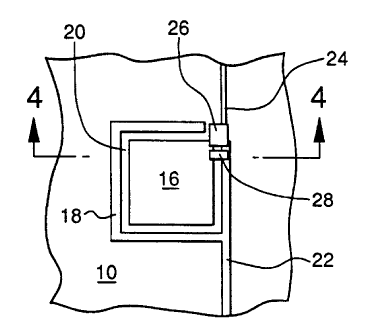
Referring to Figure 1, a single touch pad is
shown attached to a dielectric substrate 10. Substrate
has a substantially uniform thickness and can be
5 manufactured from any type of dielectric material, such
as glass, ceramic or plastic. In the preferred
embodiment, substrate 10 is manufactured from glass and
has a uniform thickness of approximately 3mm. The
thickness of substrate 10 varies with the particular
10 application such that a thicker substrate is used where
additional strength is required. If substrate 10 is
manufactured from glass, the substrate can be as thin as
approximately l.lmm and as thick as approximately 5mm.
If substrate 10 is manufactured from plastic, the
substrate can be less than lmm thick, similar to the
material used in plastic membrane switches. A thin
substrate 10 may permit the touch pad to be operated by a
user wearing a glove or mitten.
Substrate 10 has a front surface 12 and an
opposite back surface 14 (as shown in Figure 2). A user
activates the touch pad by touching front surface 12 of
substrate 10. The touch pad includes a thin, conductive
center electrode pad 16 and a thin, conductive outer
electrode 18 which substantially surrounds the center
electrode. A channel 20 is located between center
electrode 16 and outer electrode 18. Electrodes 16 and
18 are positioned such that channel 20 has a
substantially uniform width.
CA 02203695 1997-04-24
WO 96!13098 PCT/US95/13721
g _
Preferably, center electrode 16 has dimensions
such that the electrode is substantially covered by a
user's fingertip or other appendage when touched.
In the preferred embodiment, center electrode
16 is square and outer electrode 18 has a square shape
which conforms to the shape of the center electrode.
However, it will be understood that various closed,
continuous geometric shapes may also be used for the
center electrode including, but not limited to,
rectangles, trapezoids, circles, ellipses, triangles,
hexagons, and octagons. Regardless of the shape of
center electrode 16, outer electrode 18 substantially
surrounds the center electrode linearly in a spaced apart
relationship, and channel 20 has a generally uniform
width.
Preferably, center electrode 16 is a solid
conductor. However, center electrode 16 may also have a
plurality of apertures or may have a mesh or grid
pattern. It is important that center electrode 16 have a
plurality of electrical contact points in substantially
the same plane and having the same electrical potential.
As shown in Figure l, a strobe line 22 is
connected to outer electrode 18. Strobe line 22 provides
a strobe signal (shown in Figure 8) to outer electrode
18. In the preferred embodiment, the strobe signal is a
square wave oscillating between 0 and +5 volts at a
frequency between 100kHz and 200kHz. Alternatively, the
strobe signal may have a frequency less than 100kHz or
greater than 200kHz, depending on the detection circuitry
CA 02203695 1997-04-24
WO 96113098 PCT/US95/13721
- 10 -
used. Furthermore, the strobe signal may oscillate
between 0 and +3 volts, 0 and +12 volts, 0 and +24 volts,
-5 volts and +5 volts, or any other voltage range,
depending on the voltage readily available from the
device being controlled.
The strobe signal has a sharp rising edge
(shown in Figure 8) which creates a difference in the
electrical potential between outer electrode 18 and inner
electrode 16. This difference in potential between
electrodes 16 and 18 creates an arc-shaped electric field
between the electrodes, as shown by the dashed lines in
Figure 2. The electric field extends through substrate
10 and past front surface 12.
Although not shown in Figure 2, the electric
field between electrodes 16 and 18 follows a similar arc-
shaped path away from substrate 10 rather than through
the substrate. This path is a mirror image of the dashed
lines shown in Figure 2, extending downwardly rather than
upwardly.
As shown in Figure 2, the electric fields
created are in opposition to one another. For example,
the two field paths shown in Figure 2 originate from
electrode 18, at opposite sides of the pad. Since the
field paths each terminate at center electrode 16, the
paths travel toward one another. Thus, all field paths
originate at outer electrode 18 and travel inwardly
toward center electrode 16.
Referring again to Figure 1, a sense line 24 is
attached to substrate 10 adjacent outer electrode 18.
CA 02203695 1997-04-24
WO 96/13098 PCT/US95/13721
- 11 -
Sense line 24 carries a detection signal from the touch
pad to the remainder of the detection circuitry discussed
below.
As shown in Figure 3, a surface mount
transistor 26 and a surface mount resistor 28 are
electrically connected to the touch pad. Resistor 28 is
connected between center electrode 16 and outer electrode
18. In the preferred embodiment, resistor 28 has a value
of lOK ohms, thereby providing a relatively low discharge
input impedance for the touch pad.
Transistor 26 is connected between center
electrode 16, outer electrode 18 and sense line 24. In
the preferred embodiment, transistor 26 is a PNP
transistor, such as a 2N3086. The base of transistor 26
is connected to inner electrode 16, the transistor
emitter is connected to outer electrode 18, and the
transistor collector is connected to sense line 24.
Transistor 26 provides amplification and buffering of the
detection signal directly at the touch pad.
Alternatively, a NPN transistor, MOSFET, or other active
electrical component which is triggerable may be used in
place of a PNP transistor.
Figure 5 illustrates schematically a model of
the connection of transistor 26 and resistor 28 to the
touch pad. The capacitive coupling between electrodes 16
and 18 is represented in Figure 5 as a capacitor, with
resistor 28 connected in parallel with the capacitor.
Resistor 28 acts to discharge the capacitor formed by
electrodes 16 and 18. Capacitor 27 represents the
CA 02203695 1997-04-24
WO 96113098 PCT/US95/13721
- 12 -
parasitic capacitance and the results of contact by a
user. Capacitor 21 represents the parasitic capacitance
on strobe line 22. Capacitor 23 represents the parasitic
capacitance on sense line 24. A resistor 25 can be used
to compensate for differences in beta values between
different transistors and to compensate for differences
in transistor operating characteristics based on
temperature. However, in the preferred form, resistor 25
has a value of 0 ohms; i.e., no resistor 25 is used.
In the preferred embodiment, electrodes 16 and
18, strobe line 22, and sense line 24 are attached to a
flexible carrier manufactured from a polyester material
such as Consolidated Graphics No. HS-500, Type 561, Level
2, 0.005 inches thick. Electrodes 16 and 18, strobe line
22, and sense line 24 are formed using a conductive
silver ink such as Acheson No. 427 SS, 0.5 mills thick.
Transistor 26 and resistor 28 are then attached to the
electrodes and lines. A dielectric layer is placed over
the electrodes and lines to protect the conducting
surfaces. Preferably, the dielectric is Acheson No.
ML25089, 1.5 mills thick. The flexible carrier is then
bonded to substrate 10 using an adhesive such as 3M No.
467. The flexible carrier can be curved and twisted to
conform to the shape of substrate 10.
Alternatively, electrodes 16 and 18, strobe
line 22 and sense line 24 can be attached directly to
substrate 10. Transistor 26 and resistor 28 are then
attached to electrodes 16 and 18, and sense line 24.
CA 02203695 1997-04-24
WO 96113098 PCT/LTS95/13721
- 13 -
Referring to Figure 6, a matrix of touch pads
are attached to substrate 10. Each touch nac3 ;n rhP
matrix has the same configuration as the individual pad
discussed above. Also, each touch pad contains a
transistor 26 and resistor 28, as described earlier. The
touch pads are arranged into rows and columns and
attached to substrate 10. Each touch pad in a particular
column is connected to a common strobe line 22. Each
touch pad in a particular row is connected to a common
sense line 24. Thus, no two touch pads are connected to
the same combination of strobe line 22 and sense line 24.
Although Figure 6 illustrates a particular
arrangement of a touch pad matrix, it will be understood
that any number of touch pads can be arranged in any
pattern depending on the particular application. The
touch pads need not be arranged in rows and columns.
Instead, the touch pads may be randomly placed on the
substrate or arranged in a circular or diagonal manner.
The number of touch pads which can be attached to a
substrate is limited only by the size of the substrate.
Referring to Figure 7, three adjacent touch
pads are shown attached to substrate 10. The electric
field associated with each touch pad is shown with dashed
lines- As described with the individual touch pad above,
the electric field path originates at outer electrode 18
and follows an arc-shaped path outwardly through
substrate 10 and back toward center electrode 16. Since
the electric field created by each touch pad is directed
toward the center of the pad, the electric fields of
CA 02203695 1997-04-24
WO 96/13098 PCT/US95/13721
- 14 -
adjacent pads are in opposition to one another; i.e.,
moving in opposite directions. Thus, there is a reduced
chance of crosstalk between adjacent pads.
In an alternate embodiment, outer electrode 18
does not substantially surround center electrode 16. An
important feature of the arrangement of electrodes 16 and
18 is the creation of opposing electric fields. Thus, an
opposing electric field is only needed where an adjacent
touch pad exists. For example, if three touch pads are
positioned on a substrate in a linear arrangement, outer
electrodes 18 are located between adjacent pads. If the
middle pad in the three-pad arrangement has adjacent pads
to the left and right, outer electrode 18 will be located
on the left and right sides of the middle pad. However,
since no adjacent pad is located above or below the
middle pad, there is no possibility of crosstalk above or
below the middle pad. Therefore, outer electrode 18 is
not required above or below the middle pad. Similarly,
the two end pads in the three-pad arrangement have an
adjacent touch pad on one side and therefore require
outer electrode 18 only on the single adjacent side.
Referring to Figure 12, a block diagram of the
control circuit for a matrix of touch pads is shown. An
oscillator 30 produces a square wave on line 32 which
functions as the strobe signal. A demultiplexer 34
receives the strobe signal from oscillator 30. A
microprocessor 36, such as Motorola MC68HC05P9, generates
a strobe address which is provided to demultiplexer 34 on
line 38. The strobe address causes demultiplexer 34 to
CA 02203695 1997-04-24
WO 96113098 PCT/US95/13721
- 15 -
select one of several output lines which receives the
strobe signal. Each output line from demultiplexer 34 is
connected to one strobe line 22 for a particular column
of touch pads. Thus, the output from oscillator 30 is
connected via demultiplexer 34 to strobe line 22 for a
particular column of touch pads.
Microprocessor 36 also generates a sense
address which is provided to multiplexer 46 on line 48.
The sense address causes multiplexer 46 to select one of
several input lines which will be monitored as the sense
line. Each input line represents the sense line 24 for a
particular row of touch pads. Thus, a particular touch
pad in the matrix can be selectively monitored by
"strobing" a column of pads, and "sensing" a row of pads.
Alternatively, the matrix of touch pads can be arranged
such that monitoring is accomplished by "strobing" a row
of pads and "sensing" a column of pads.
Sense line 24 selected by multiplexer 46 is
connected to a peak detector and amplifier circuit 52
using line 50. The output of circuit 52 is provided to
microprocessor 36 on line 54. Depending on the signal
received from circuit 52, an algorithm running on
microprocessor 36 determines whether a controlled device
58 should be activated, deactivated or adjusted.
The peak detector and amplifier circuits shown
in Figure 13 are used in either a single touch pad design
or a multiple touch pad design; e.g., a matrix of touch
pads. The left portion of Figure 13 represents the peak
detector circuit and the right portion of Figure 13
CA 02203695 1997-04-24
WO 96/13098 PCT/US95/13721
- 16 -
represents the amplifier circuit. The detection signal
is carried by sense line 24 to the non-inverting input of
operational amplifier 64. A resistor 62 is connected
between sense line 24 and ground. Preferably, resistor
62 has a value of lOK ohms. A pull-up resistor 66 is
connected between +5 volts and the output of operational
amplifier 64. In the preferred embodiment, resistor 66
has a value of lOK ohms. The output of operational
amplifier 64 is connected through diode 67 to the
inverting input of operational amplifier 64. A resistor
68 and capacitor 70 are connected in parallel between
ground and the inverting input of operational amplifier
64. Preferably, operational amplifiers 64 and 72 are of
the type LM339.
The non-inverting input of operational
amplifier 72 receives the output signal from the peak
detector circuit. A pull-up resistor 74 is connected
between +5 volts and output 82 of operational amplifier
72. In the preferred embodiment, resistor 74 has a value
of lOK ohms. Output 82 is connected through a resistor
78 to the inverting input of operational amplifier 72. A
resistor 76 is connected between the inverting input of
operational amplifier 72 and ground. A capacitor 80 is
connected between output 82 and ground.
The value of resistors 76 and 78 determine the
level of amplification by the amplifier circuit. In the
preferred embodiment, resistor 76 has a value of 66K ohms
and resistor 78 has a value of 100K ohms. If a different
level of amplification is desired, different values are
CA 02203695 1997-04-24
WO 96/13098 PCT/US95/13721
- 17 -
used for resistors 76 and 78, as will be known to those
skilled in the art. Furthermore, detection circuitry may
be used which does not require the use of an amplifier
connected to the peak detector output. Such a detection
circuit will be known to those skilled in the art.
In operation, the touch pad is activated when a
user contacts substrate 10. The touch pad will sense
contact by a fingertip or other appendage which causes
sufficient disruption of the electric field, such as a
knuckle, palm or elbow.
The strobe signal shown in Figure 8 is applied
to strobe line 22, which is connected to outer electrode
18. Preferably, the strobe signal has a rise time of
approximately 7 nsec. However, rise times up to 110 nsec
may also be used. Faster rise times, such as 7 nsec,
provide lower input impedances and are therefore
preferred. The strobe signal creates an electric field
at the touch pad, as described earlier. When substrate
10 is not being touched, the waveform shown in Figure 9
is present on sense line 24. The rising edge of each
strobe signal pulse turns on transistor 26, causing the
transistor to draw base current. The capacitor formed by
electrodes 16 and 18 then discharges through resistor 28
until the next pulse arrives.
The base current of transistor 26 is determined
by the equation IH=C(dV/dT) where IB is the base current,
C is the capacitance of the touch pad, and dV/dT is the
change in voltage with respect to time. The change in
voltage with respect to time is created by the change in
CA 02203695 1997-04-24
WO 96113098 PCT/US95/13721
- 18 -
voltage level of the oscillating strobe signal. When a
user contacts the touch pad formed by electrodes 16 and
18, the capacitive charge of the touch pad is reduced
while the capacitive charge of parasitic capacitor 27 is
increased.
Transistor 26 amplifies and buffers the
detection signal at each touch pad. This reduces the
difference in signal level between touch pads caused by
different lead lengths and lead routing paths. By
providing a more uniform detection signal level, greater
amplification is possible while maintaining the signal
level between 0 and +5 volts.
The waveform shown in Figure 9 is applied to
the peak detector circuit shown in Figure 13. The output
of the peak detector when not being touched is shown in
Figure 10. The output of the peak detector when touched
by a user is shown in Figure 11. As illustrated in
Figures 10 and 11, the waveform has the same shape but a
different amplitude. Thus, when a user touches the touch
pad, the output of the peak detector is altered.
When using a matrix of touch pads, a control
circuit (as shown in Figure 12) is used to selectively
monitor each touch pad in the matrix. Microprocessor 36
sequentially selects each strobe line 22 and each sense
line 24 by sending the appropriate strobe address and
sense address to the demultiplexer and multiplexer,
respectively. Each sense line 24 is monitored by peak
detector 52 which amplifies the detection signal and
transmits it to microprocessor 36.
CA 02203695 1997-04-24
WO 96/13098 PCT/US95/13721
- 19 -
Figures 14a and 14b illustrate a flowchart for
a program which monitors a matrix of touch pads. The
program monitors one touch pad at a time and sequentially
scans all touch pads in the matrix. The program begins
at block 100 when an interrupt is received. Step 102
checks to determine whether or not the system has just
been turned on (cold-started). If the system is being
cold-started, step 104 initializes all variables and step
106 resets the strobe and sense counters.
If the system has not been cold-started, then
step 108 retrieves the detection signal level. Next,
step 110 determines whether the average values have been
initialized. An average voltage level is stored for each
touch pad to determine the average "non-touched"
detection signal level.
If the average values have been initialized,
then the program jumps to step 114 to determine the
difference between the average detection signal level and
the current detection signal level. If the average
values have not been initialized, then the current
detection signal level is stored as the average value for
the particular pad being monitored.
At step 116, if the current detection signal
level is less than the average value then the program
branches to step 128. At step 128, if the average flag
is set then the average flag is decremented. The average
flag indicates whether or not the particular signal will
be averaged. Since only "non-touched" signals are
averaged, the average flag will be set only when a "non-
CA 02203695 1997-04-24
WO 96!13098 PCT/US95113721
- 20 -
touched" condition is sensed. After decrementing the
average value, the pad status is set to inactive (non-
touched) at step 126.
At step 116, if the current detection signal
level is not less than the average value then step 118
determines whether the difference is greater than a
predetermined setpoint. The setpoint is a threshold
difference level which must be reached to indicated a
"touched" condition. If the difference is greater than
the setpoint, then the pad status is set active (touched)
at step 120.
If the difference at step 118 is not greater
than the setpoint, then the program branches to step 122
to determine whether the average flag is set. If the
average flag is not set, the program branches to step 126
and sets the pad status to inactive (non-touched). If
the average flag is set, the average value is incremented
at step 124 and the pad status is set inactive at step
126.
At step 132, the program determines whether the
last strobe line is being sensed. If the current strobe
line being sensed is not the last strobe line, then the
strobe pointer is incremented at step 134 and jumps to
step 158 where a new strobe address and sense address is
selected. If the current strobe line being sensed is the
last strobe line, then the strobe pointer is reset at
step 136. At step 138, the program determines whether
the current sense line is the last sense line. If not,
CA 02203695 1997-04-24
WO 96!13098 PCT/US95/13721
- 21 -
step 140 increments the sense pointer and jumps to step
158.
If the current sense line is the last sense
line, then a complete scan of the matrix has been
completed and step 142 resets the sense pointer. Step
144 clears the average flag and step 146 increments the
average flag counter. If step 148 determines that the
average flag counter is not full, then the program
branches to step 154. If the average flag counter is
full, then the counter is reset at step 150 and the
average flag is set at step 152.
At step 154, the status of the touch pad being
monitored is output from the microprocessor to the
remaining control circuitry. Step 156 resets all
variables, causing the program to begin scanning at the
beginning of the matrix. After all variables have been
reset, step 158 selects the new strobe line and sense
line to be monitored. Step 160 returns the program to
step 100 to wait for the next interrupt.