Language selection

Search

Patent 2203725 Summary

Third-party information liability

Some of the information on this Web page has been provided by external sources. The Government of Canada is not responsible for the accuracy, reliability or currency of the information supplied by external sources. Users wishing to rely upon this information should consult directly with the source of the information. Content provided by external sources is not subject to official languages, privacy and accessibility requirements.

Claims and Abstract availability

Any discrepancies in the text and image of the Claims and Abstract are due to differing posting times. Text of the Claims and Abstract are posted:

  • At the time the application is open to public inspection;
  • At the time of issue of the patent (grant).
(12) Patent: (11) CA 2203725
(54) English Title: METHOD OF TRANSMITTING CLOCK SIGNAL AND DEVICE EMPLOYING THE SAME
(54) French Title: METHODE DE TRANSMISSION DE SIGNAUX D'HORLOGE ET DISPOSITIF UTILISANT CETTE METHODE
Status: Deemed expired
Bibliographic Data
(51) International Patent Classification (IPC):
  • H04L 7/04 (2006.01)
  • H03K 5/00 (2006.01)
  • H04L 7/00 (2006.01)
  • H04L 7/033 (2006.01)
(72) Inventors :
  • FUGO, MASATOSHI (Japan)
(73) Owners :
  • NEC CORPORATION (Japan)
(71) Applicants :
  • NEC CORPORATION (Japan)
(74) Agent: G. RONALD BELL & ASSOCIATES
(74) Associate agent:
(45) Issued: 2001-07-03
(22) Filed Date: 1997-04-25
(41) Open to Public Inspection: 1997-11-21
Examination requested: 1997-04-25
Availability of licence: N/A
(25) Language of filing: English

Patent Cooperation Treaty (PCT): No

(30) Application Priority Data:
Application No. Country/Territory Date
125777/1996 Japan 1996-05-21

Abstracts

English Abstract


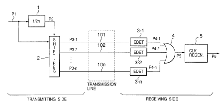
A frequency divider 1 on the transmitting side
divides the frequency of a clock signal of period T by 8,
generates a pulse signal P2 of pulse width 4T and duty
ratio 50%, and outputs the result to a shift register 2.
The shift register 2 generates pulse signals P3-1, P3-2,
P3-3, and P3-4 by giving delays 0, T, 2T, and 3T to the
pulse signal P2, and sends them to transmission lines
101, 102, 103, and 104, respectively. Edge detectors
3-1, 3-2, 3-3, and 3-4 on the receiving side detect
respectively the leading edges and the trailing edges
of the pulse signals P3-1, P3-2, P3-3, and P3-4, and
output edge detection signals P4-1, P4-2, P4-3, and P4-4.
An OR gate 4 combines these edge detection signals.
A clock regenerator 5 generates a regenerated signal P6
having the frequency equal to that of the clock signal P1
based on the combined edge detection signal P5.


French Abstract

Un diviseur de fréquence 1 incorporé à un émetteur divise la fréquence d'un signal d'horloge de période T par 8, produit une impulsion P2 de largeur 4T à rapport cyclique de 50 % et transmet le résultat à un registre à décalage 2. Celui-ci produit des impulsions P3-1, P3-2, P3-3 et P3-4 en produisant des retards de 0, T, 2T et 3T dans l'impulsion P2, et les transmet aux lignes de transmission 101, 102, 103 et 104 respectivement. Des détecteurs de flancs d'impulsion 3-1, 3-2, 3-3 et 3-4 incorporés au récepteur détectent respectivement les flancs avant et les flancs arrière des impulsions P3-1, P3-2, P3-3 et P3-4 et produisent des signaux de détection de flancs d'impulsion P4-1, P4-2, P4-3 et P4-4. Une porte OU 4 combine ces signaux de détection de flancs d'impulsion. Un régénérateur de signaux d'horloge 5 produit un signal d'horloge régénéré P6 dont la fréquence est égale à celle du signal d'horloge P1 en utilisant le signal combiné de détection de flancs d'impulsion P5.

Claims

Note: Claims are shown in the official language in which they were submitted.


-7-
THE EMBODIMENTS OF THE INVENTION IN WHICH AN EXCLUSIVE
PROPERTY OR PRIVILEGE IS CLAIMED ARE DEFINED AS FOLLOWS:
1. A clock signal transmission equipment for
transmitting a clock signal of period T from a transmitting
side to a receiving side, wherein,
said transmitting side comprises:
frequency dividing means which generates a first
pulse signal of duty ratio 50% and pulse width nT (n being
a nonzero positive integer) obtained by dividing the
frequency of said clock signal of period T by 2n; and
transmission pulse generating means which generates
n pieces of second pulse signals by giving delays of 0, T,
2T, ..., and (n-1)T to said first pulse signal,
and said receiving side comprises:
pulse detecting means which receives respective
members of said n pieces of second pulse signals, detects
the leading edge and the trailing edge of these n pieces of
second pulse signals, and generates a third pulse signal
which shows the leading edges and the trailing edges of all
of these n pieces of second pulse signals; and
clock regenerating means which regenerates said
clock signal of period T based on said third pulse signal.
2. The clock signal transmission equipment as
claimed in claim 1, wherein said transmission pulse
generating means comprises a shift register which receives


-8-
said first pulse signal at its data input terminal and
receives said clock signal of period T to its clock input
terminal.
3. The clock signal transmission equipment as
claimed in claim 1, wherein said pulse detecting means
comprises n pieces of edge detection circuits which receive
respective members of said n pieces of second pulse signals
and generate detection signals by detecting the leading
edges and the trailing edges of the received second pulse
signals, and a logic circuit which generates said third
pulse signal by combining the detection signals received
from said n pieces of edge detection circuits.
4. A method of transmitting a clock signal of
period T from a transmitting side to a receiving side,
wherein
said transmitting side generates a first pulse
signal of duty ratio 50o and pulse width nT by dividing the
frequency of said clock signal of period T by 2n (n being a
nonzero positive integer); and generates n pieces of second
pulse signals by giving delays of 0, T, 2T, ..., and (n-1)T
to said first pulse signal, and
said receiving side receives said n pieces of
second pulse signals; generates a third pulse signal
showing the leading edges and the training edges of said n
pieces of the second pulse signals by detecting the leading


-9-
edges and the trailing edges of these n pieces of second
pulse signals; and regenerates said clock signal of period
T based on said third pulse signal.

Description

Note: Descriptions are shown in the official language in which they were submitted.


CA 02203725 2000-06-08
- 1 -
METHOD OF TRANSMITTING CLOCK SIGNAL AND
DEVICE EMPLOYING THE SAME
The present invention relates to a clock signal
transmission technique, and more particularly to a high
frequency clock signal transmission technique.
In recent years, in order to increase the data
transfer rate, a tendency of increasing the frequency of
the clock signal, which indicates the timing of the
transfer data and is transmitted along with the data, is
recognizable. However, as the frequency of the transmitted
clock signal goes up, the clock signal on the transmission
line undergoes a waveform distortion which gives rise to
variations in the pulse width or the duty ratio. The
variations in the pulse width or the duty ratio are
responsible for the data transfer errors.
A technique for resolving such a problem is
disclosed in Japanese Laid-Open Patent Publication No. H4-
10011. According to the technique disclosed in the
publication, the transmitting side sends two signals,
namely, a clock signal and its inverted signal, to the
receiving side via respective transmission lines. On the
receiving side, the two received signals are respectively
frequency divided by 2, and the clock signal on the
receiving side is obtained by subjecting these signals
frequency divided by 2 to the exclusive OR operation.
However, according to this prior art, as the
frequency of the clock signal becomes higher, waveform


CA 02203725 2000-06-08
- 2 -
distortions occur in the clock signal as well as in the
inverted signal, which makes it difficult to know precisely
the reception timings of data which are sent along with the
clock signal.
The main object of the present invention is to
provide a clock signal transmission method, and a device
adopting the same, which can mitigate the effect of the
waveform distortion on the transmission lines even when the
frequency of the transmitted clock signal becomes high.
The present invention consists of a clock signal
transmission equipment for transmitting a clock signal of
period T from a transmitting side to a receiving side,
wherein, said transmitting side comprises: frequency
dividing means which generates a first pulse signal of duty
ratio 50% and pulse width nT (n being a nonzero positive
integer) obtained by dividing the frequency of said clock
signal of period T by 2n; and transmission pulse generating
means which generates n second pulse signals by giving
delays of 0, T, 2T, ..., and (n-1)T to said first pulse
signal, and said receiving side comprises: pulse detecting
means which receives respective ones of said n second pulse
signals, detects the leading edge and the trailing edge of
these n second pulse signals, and generates a third pulse
signal which shows the leading edges and the trailing edges
of all of these n second pulse signals; and clock
regenerating means which regenerates said clock signal of
period T based on said third pulse signal.


CA 02203725 2000-06-08
- 3 -
In accordance with this invention, on the
transmitting side, a transmitting side clock signal of
period T is frequency divided by 2n (n is a nonzero
integer) to convert it to a first pulse signal of period
2nT, and n second pulse signals are generated by giving
delays of 0, T, 2T, ..., and (n-1)T to the first pulse
signal and these n second pulse signals are transmitted via
a plurality of transmission lines.
On the receiving side, these n second pulse signals
are received to detect the leading edges and trailing edges
of these pulse signals, and the receiving side clock signal
is generated based on timing signals that show the leading
and trailing edges of these n second pulse signals.
In this invention, the waveform distortion is made
less likely to occur on the transmission lines since the
frequencies of the n pulse signals transmitted via the
transmission lines are 1/2n of the frequency of the
transmitting side clock signal. Consequently, this
invention is capable of generating the receiving side clock
signal with more precise timings than in the prior art.
The invention, as exemplified by a preferred
embodiment, is described with reference to the drawings in
which:
Figure 1 is a block diagram showing an embodiment
of the invention; and
Figure 2 is a timing chart showing an example of
each of the signals shown in Figure 1.


CA 02203725 2000-06-08
- 4 -
Referring to Figure 1, the equipment on the
transmitting side includes a frequency divider 1 which
divides the frequency of a transmitting side clock signal
P1 by 2n and outputs a first pulse signal P2; and a shift
register 2 which receives the first pulse signal P2,
generates n second pulse signals P3-l, P3-2, ..., and P3-n
by giving delays 0, T, 2T, ..., and (n-1)T to the first
pulse signal P2, based on the clock signal P1 on the
transmitting side, and outputs them to transmission lines
101, 102, ..., and lOn, respectively.
On the transmitting side, the frequency divider 1
divides the frequency of the clock signal P1 with period T
by 2n to generate a first pulse signal P2 of pulse width nT
and duty ratio 50%, and outputs it to the shift register 2.
The shift register 2 having n output terminals generates n
second pulse signals P3-1, P3-2, ..., and P3-n by giving
delays 0, T, 2T, ..., and (n-1)T to the first pulse signal
P2, and outputs them from n output terminals to the
transmission lines 101, 102, ..., and lOn.
Figure 2 shows the timings of respective signals
for the case of n=4. In this case, the frequency of the
clock signal P1 with period T is divided by 2 x 4 by the
frequency divider 1 to convert it to a first pulse signal
P1 of pulse width 4T and duty ratio 50%. In response to
the input clock signal P1, the shift register 2
sequentially shifts the first pulse signal P2 to generate n
second pulse signals P3-1, P3-2, P3-3, and P3-4 by delaying


CA 02203725 2000-06-08
- 5 -
the first pulse signal P1 by 0, T, 2T, and 3T,
respectively, and outputs them to 4 transmission lines 101,
102, 103, and 104, respectively.
On the other hand, referring to Figure 1, the
receiving side equipment includes n edge detectors 3-1, 3-
2, ..., and 3-n which detect the leading edges and the
trailing edges of the reception signals P3-1, P3-2, ...,
and P3-n supplied by the transmission lines 101, 102, ...,
and lOn, and output edge detection signals P4-l, P4-2, ...,
and P4-n; a logic circuit 4 which generates a third pulse
signal P5 by combining the edge detection signals P4-1, P4-
2, ..., and P4-n; and a clock regenerator 6 which generates
a regenerated clock signal P6 based on the third pulse
signal P5.
The clock regenerator 5 has a built-in phase locked
loop (PLL), controls the oscillation frequency of a voltage
controlled oscillator (VCO) within the PLL based on the
third pulse signal P5, and generates a regenerated clock
signal P6 which has the same frequency as that of the clock
signal P1.
Referring again to Figure 2, the edge detectors 3-
1, 3-2, 3-3, and 3-4 receive the second pulse signals P3-1,
P3-2, P3-3, and P3-4, transmitted through the transmission
lines 101, 102, 103, and 104, respectively, and output edge
detection signals P4-1, P4-2, P4-3, and P4-4 by detecting
respective leading edges and trailing edges of the second
pulse signals. These edge detection signals are combined


CA 02203725 2000-06-08
- 6 -
by an OR circuit 4 and the result is output as the third
pulse signal P5. The frequency of this timing signal P5
agrees with the frequency of the transmitting side clock
signal Pl. This timing signal P5 is supplied to the clock
regenerator 5 having the built-in PLL which generates the
receiving side clock signal P6 of duty ratio 500.
As described in the above, according to this
invention a clock signal having a frequency 1/T is
frequency-divided by 2n to generate a pulse signal of
frequency 1/2nT and duty ratio of 50%. The pulse signal of
frequency 1/2nT is delayed by 0, T, 2T, ..., and (n-1)T and
the resulting signals are transmitted via n transmission
lines. In this way, it is possible to transmit a clock
signal by alleviating the influence of waveform distortion
which is generated on the transmission lines.
Modifications of the invention herein disclosed
will occur to a person skilled in the art and all such
modifications are deemed to be within the scope of the
invention as defined by the appended claims.

Representative Drawing
A single figure which represents the drawing illustrating the invention.
Administrative Status

For a clearer understanding of the status of the application/patent presented on this page, the site Disclaimer , as well as the definitions for Patent , Administrative Status , Maintenance Fee  and Payment History  should be consulted.

Administrative Status

Title Date
Forecasted Issue Date 2001-07-03
(22) Filed 1997-04-25
Examination Requested 1997-04-25
(41) Open to Public Inspection 1997-11-21
(45) Issued 2001-07-03
Deemed Expired 2003-04-25

Abandonment History

There is no abandonment history.

Payment History

Fee Type Anniversary Year Due Date Amount Paid Paid Date
Request for Examination $400.00 1997-04-25
Registration of a document - section 124 $100.00 1997-04-25
Application Fee $300.00 1997-04-25
Maintenance Fee - Application - New Act 2 1999-04-26 $100.00 1999-04-16
Maintenance Fee - Application - New Act 3 2000-04-25 $100.00 2000-04-20
Final Fee $300.00 2001-04-05
Maintenance Fee - Application - New Act 4 2001-04-25 $100.00 2001-04-17
Owners on Record

Note: Records showing the ownership history in alphabetical order.

Current Owners on Record
NEC CORPORATION
Past Owners on Record
FUGO, MASATOSHI
Past Owners that do not appear in the "Owners on Record" listing will appear in other documentation within the application.
Documents

To view selected files, please enter reCAPTCHA code :


To view images, click a link in the Document Description column. To download the documents, select one or more checkboxes in the first column and then click the "Download Selected in PDF format (Zip Archive)" or the "Download Selected as Single PDF" button.

List of published and non-published patent-specific documents on the CPD .

If you have any difficulty accessing content, you can call the Client Service Centre at 1-866-997-1936 or send them an e-mail at CIPO Client Service Centre.


Document
Description 
Date
(yyyy-mm-dd) 
Number of pages   Size of Image (KB) 
Representative Drawing 2001-06-27 1 6
Cover Page 1997-12-31 1 53
Drawings 2000-06-08 2 25
Claims 2000-06-08 3 82
Description 2000-06-08 6 221
Abstract 1997-04-25 1 23
Description 1997-04-25 6 188
Claims 1997-04-25 3 70
Drawings 1997-04-25 2 22
Cover Page 2001-06-27 1 36
Representative Drawing 1997-12-31 1 5
Fees 2000-04-20 1 41
Correspondence 2001-04-05 1 29
Fees 2001-04-17 1 43
Assignment 1997-04-25 6 171
Prosecution-Amendment 2000-03-08 2 4
Prosecution-Amendment 2000-06-08 14 524
Fees 1999-04-16 1 45