Language selection

Search

Patent 2204136 Summary

Third-party information liability

Some of the information on this Web page has been provided by external sources. The Government of Canada is not responsible for the accuracy, reliability or currency of the information supplied by external sources. Users wishing to rely upon this information should consult directly with the source of the information. Content provided by external sources is not subject to official languages, privacy and accessibility requirements.

Claims and Abstract availability

Any discrepancies in the text and image of the Claims and Abstract are due to differing posting times. Text of the Claims and Abstract are posted:

  • At the time the application is open to public inspection;
  • At the time of issue of the patent (grant).
(12) Patent Application: (11) CA 2204136
(54) English Title: SILICON-ON-INSULATOR DEVICE WITH FLOATING COLLECTOR
(54) French Title: DISPOSITIF A SILICON SUR ISOLATEUR A COLLECTEUR FLOTTANT
Status: Dead
Bibliographic Data
(51) International Patent Classification (IPC):
  • H01L 29/72 (2006.01)
  • H01L 29/08 (2006.01)
  • H01L 29/73 (2006.01)
(72) Inventors :
  • ARNBORG, TORKEL BENGT (Sweden)
(73) Owners :
  • TELEFONAKTIEBOLAGET LM ERICSSON (PUBL) (Not Available)
(71) Applicants :
  • TELEFONAKTIEBOLAGET LM ERICSSON (Sweden)
(74) Agent: MARKS & CLERK
(74) Associate agent:
(45) Issued:
(86) PCT Filing Date: 1995-10-31
(87) Open to Public Inspection: 1996-05-09
Examination requested: 2002-08-20
Availability of licence: N/A
(25) Language of filing: English

Patent Cooperation Treaty (PCT): Yes
(86) PCT Filing Number: PCT/SE1995/001284
(87) International Publication Number: WO1996/013862
(85) National Entry: 1997-04-30

(30) Application Priority Data:
Application No. Country/Territory Date
9403722-3 Sweden 1994-10-31

Abstracts

English Abstract


In a semiconductor device comprising a silicon substrate (1), an insulating
layer (2) on said silicon substrate (1), a silicon layer (3) on said
insulating layer (2), said silicon layer (3) being weakly doped with
impurities of a first conduction type (N), a base region (4) extending into
said silicon layer (3) form the free surface thereof, said base region (4)
being doped with impurities of a second conduction type (P), an emitter region
(5), extending into said base region (4) from the free surface thereof, said
emitter region (5) being heavily doped with impurities of said first
conduction type (N), and at least one collector region (6) extending into said
silicon layer (3) from the free surface thereof at a lateral distance from
said base region (4), said collector region (6) being doped with impurities of
said first conduction type (N), a floating collector region (7) being provided
in said silicon layer (3) between said insulating layer (2) and said base
region (4) at a distance from said base region (4), the lateral extension of
said floating collector region (7) being larger than that of the emitter
region (5) and smaller than that of the base region (4), said floating
collector region (7) being more doped with impurities of said first conduction
type (N) than said silicon layer (3).


French Abstract

Dans un dispositif à semi-conducteur comprenant un substrat en silicium (1), une couche isolante (2) sur ledit substrat en silicium (1), une couche de silicium (3) sur ladite couche isolante (2), ladite couche de silicium (3) étant faiblement dopée avec des impuretés d'un premier type de conduction (N), une région de base (4) s'étendant dans ladite couche de silicium (3) à partir de la surface libre de celle-ci, ladite région de base (4) étant dopée avec des impuretés d'un second type de conduction (P), une région émettrice (5) s'étendant dans ladite région de base (4) à partir de la surface libre de celle-ci, ladite région émettrice (5) étant lourdement dopée avec des impuretés dudit premier type de conduction (N) et au moins une région collectrice (6) s'étendant dans ladite couche de silicium (3) à partir de la surface libre de celle-ci à une distance latérale de ladite région de base (4), ladite région collectrice (6) étant dopée avec des impuretés dudit premier type de conduction (N), une région de collectrice flottante (7) étant prévue dans ladite couche de silicium (3) entre ladite couche isolante (2) et ladite région de base (4) à une certaine distance de ladite région de base (4), l'extension latérale de ladite région collectrice flottante (7) étant plus grande que celle de la région émettrice (5) et plus petite que celle de la région de base (4), ladite région collectrice flottante (7) étant plus dopée avec des impuretés du premier type de conduction (N) que ladite couche de silicium (3).

Claims

Note: Claims are shown in the official language in which they were submitted.


5
CLAIM

A semiconductor device comprising
- a silicon substrate (1),
- an insulating layer (2) on said silicon substrate (1),
- a silicon layer (3) on said insulating layer (2), said
silicon layer (3) being weakly doped with impurities of a
first conduction type (N),
- a base region (4) extending into said silicon layer (3)
from the free surface thereof, said base region (4) being
doped with impurities of a second conduction type (P),
- an emitter region (5), extending into said base region (4)
from the free surface thereof, said emitter region (5) being
heavily doped with impurities of said first conduction type
(N), and
- at least one collector region (6) extending into said
silicon layer (3) from the free surface thereof at a lateral
distance from said base region (4), said collector region (6)
being doped with impurities of said first conduction type
(N), characterized by
- a floating collector region (7) being provided in said
silicon layer (3) between said insulating layer (2) and said
base region (4) at a distance from said base region (4), the
lateral extension of said floating collector region (7) being
larger than that of the emitter region (5) and smaller than
that of the base region (4), said floating collector region
(7) being more doped with impurities of said first conduction
type (N) than said silicon layer (3).

Description

Note: Descriptions are shown in the official language in which they were submitted.


CA 02204136 1997-04-30
W 096/13862 ~ h~ 284

SILICON-ON-INSULATOR DEVICE WITH FLOATING COLLECTOR
I~ECEC~IC~iL FIELD
The invention relates to a semiconductor device
comprising a silicon substrate, an insulating layer on said
silicon substrate, a silicon layer on said insulating layer,
said silicon layer being weakly doped with impurities of a
- first conduction type, a base region extending into said
silicon layer from the free surface thereof, said base region
being doped with impurities of a second conduction type, an
emitter region, extending into said base region from the free
surface thereof, said emitter region being heavily doped with
impurities of said first conduction type, and at least one
collector region extending into said silicon layer from the
free surface thereof at a lateral distance from said base
region, said collector region being doped with impurities of
said first conduction type.

BACKGRO~ND OF THE lNv~N-~lON
A bipolar silicon-on-insulator transistor having
the above structure, is known from Andrej Litwin and Torkel
Arnborg: "Bxtremely compact CMOS compatible bipolar silicon-
on-insulator transistor for mixed high voltage and high
density integrated circuit applications", Late News Paper at
ESSDERC'93, Sept., 1993, and Andrej Litwin and Torkel
Arnborg: "Compact Very High Voltage Compatible Bipolar
Silicon-On-Insulator Transistor", ISPSD'93, Davos, June,
1994.
The emitter-base structure of such a transistor, is
vertical but the high collector voltage is supported by a
lateral fully depleted collector region. The transistor can
be designed to handle almost any desired voltage up to
several hundred volts.
One important feature of a high speed transistor is
the unity gain frequency. This frequency is the inverse sum
of the relevant transit times in the transistor. In the known
silicon-on-insulator transistor the most important transit
times are those required for vertical transport across the
base and for lateral transport along the silicon-oxide

CA 02204136 1997-04-30
WO96/13862 PCT/SE95/01~


interface. The physical transport mechanism is in most cases
diffusion and not drift implying that the transit times are
proportional to the inverse square of the transport distance.
Since the lateral distance at the interface is larger than
the vertical distance in the base the associated transit time
is much larger. The speed of the transistor is thus mainly
limited by the transit time at the interface.

DISCLOS~RE OF T~E lNV~NLlON
The object of the invention is to eliminate the
limitations on speed imposed by the lateral diffusion along
the silicon-oxide interface and bring about a high speed
transistor without affecting its high voltage capability.
This is accomplished by the invention in a
semiconductor device of the above type by a floating
collector region being provided in said silicon layer between
said insulating layer and said base region at a distance from
said base region, the lateral extension of said floating
collector region being larger than that of the emitter region
and smaller than that of the base region, said floating
collector region being more doped with impurities of said
first conduction type than said silicon layer.

BRIEF DESCRIPTION OF DRAWING
The invention will be described more in detail with
reference to the appended drawing on which the single figure
shows an embodiment of a bipolar silicon-on-insulator
transistor according to the invention.

DESCRIPTION OF PREFERRED EMBODIMENTS
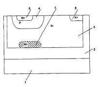
The single figure on the drawing shows an
embodiment of a bipolar silicon-on-insulator (SOI) transistor
according to the invention. The transistor comprises a
silicon substrate l on which an insulating oxide layer 2 is
3 5 provided.
A silicon layer 3 which is weakly doped with
impurities of conduction type N, is provided on the

CA 02204136 1997-04-30
W096/13862 PCTISE95/01~4


insulating oxide layer 2.
A base region 4 which is doped with impurities of
conduction type P, extends into the silicon layer 3 from the
free sur~ace thereof.
An emitter region 5 which is heavily doped with
impurities of conduction type N, extends into the base region
4 from the free surface thereof.
In the embodiment shown, the transistor comprises
one collector region 6 which is doped with impurities of
conduction type N. The collector region extends into the
silicon layer 3 from the free surface thereof at a lateral
distance from the base region 4.
In another embodiment (not shown), the transistor
may comprise two collector regions located on either side of
the base region.
As mentioned above, the transport of carriers along
the interface between the silicon layer 3 and the oxide layer
2 below the base 4 and the emitter 5, is mainly diffusion,
and the associated transit time is limiting the speed of the
transistor substantially.
However, according to the invention, by inserting a
floating collector region 7 selectively below the base 4 and
the emitter 5 the high speed limited by the base-emitter
structure, is achievable without affe-ting the high voltage
capability.
In accordance with the invention, the floating
collector region 7 is provided in the silicon layer 3 between
the insulating oxide layer 2 and the base region 4 at a
distance from the base region 4. The lateral extension of the
floating collector region 7 is larger than the lateral
extension of the emitter region 5 and smaller than the
lateral extension of the base region 4. Also according to the
invention, the floating collector region 7 is more doped with
impurities of conduction type N than the silicon layer 3.
By adding the highly doped N-type floating
collector region 7 below the base 4 and the emitter 5, the
limiting transit time was reduced to almost zero without

CA 02204136 1997-04-30
W 096/13862 PCT/SE9~01284

affecting the high voltage capability. Thus, a unique
combination of very high speed and very high voltage devices
can be realized in a single process with only layout
variations.


Representative Drawing
A single figure which represents the drawing illustrating the invention.
Administrative Status

For a clearer understanding of the status of the application/patent presented on this page, the site Disclaimer , as well as the definitions for Patent , Administrative Status , Maintenance Fee  and Payment History  should be consulted.

Administrative Status

Title Date
Forecasted Issue Date Unavailable
(86) PCT Filing Date 1995-10-31
(87) PCT Publication Date 1996-05-09
(85) National Entry 1997-04-30
Examination Requested 2002-08-20
Dead Application 2004-11-01

Abandonment History

Abandonment Date Reason Reinstatement Date
2003-10-31 FAILURE TO PAY APPLICATION MAINTENANCE FEE

Payment History

Fee Type Anniversary Year Due Date Amount Paid Paid Date
Application Fee $300.00 1997-04-30
Registration of a document - section 124 $100.00 1997-10-02
Maintenance Fee - Application - New Act 2 1997-10-31 $100.00 1997-10-20
Maintenance Fee - Application - New Act 3 1998-11-02 $100.00 1998-10-21
Maintenance Fee - Application - New Act 4 1999-11-01 $100.00 1999-10-14
Maintenance Fee - Application - New Act 5 2000-10-31 $150.00 2000-10-19
Maintenance Fee - Application - New Act 6 2001-10-31 $150.00 2001-10-18
Request for Examination $400.00 2002-08-20
Maintenance Fee - Application - New Act 7 2002-10-31 $150.00 2002-10-23
Owners on Record

Note: Records showing the ownership history in alphabetical order.

Current Owners on Record
TELEFONAKTIEBOLAGET LM ERICSSON (PUBL)
Past Owners on Record
ARNBORG, TORKEL BENGT
Past Owners that do not appear in the "Owners on Record" listing will appear in other documentation within the application.
Documents

To view selected files, please enter reCAPTCHA code :


To view images, click a link in the Document Description column. To download the documents, select one or more checkboxes in the first column and then click the "Download Selected in PDF format (Zip Archive)" or the "Download Selected as Single PDF" button.

List of published and non-published patent-specific documents on the CPD .

If you have any difficulty accessing content, you can call the Client Service Centre at 1-866-997-1936 or send them an e-mail at CIPO Client Service Centre.


Document
Description 
Date
(yyyy-mm-dd) 
Number of pages   Size of Image (KB) 
Representative Drawing 1997-08-08 1 3
Cover Page 1997-08-08 1 67
Abstract 1997-04-30 1 35
Description 1997-04-30 4 154
Claims 1997-04-30 1 36
Drawings 1997-04-30 1 9
Assignment 1997-04-30 2 99
PCT 1997-04-30 15 528
Correspondence 1997-06-03 1 37
Assignment 1997-10-02 2 70
Prosecution-Amendment 2002-08-20 1 29