Note: Descriptions are shown in the official language in which they were submitted.
CA 02204268 1997-0~-01
WO g6/15563 1 ~ u~g5ll4s43
SMART BATTERY DEVICE
i 1
1. Field of the Invention
The present invention relates to generally to
the art of rechargeable batteri~s and more specifically
5 to a smart battery for use in an intelligent device
having power management capabilities. The invention is
a smart battery apparatus for controlling the operation
of rechargeable Nickel Metal ~ydride (NiMH) or Nickel
Cadmium (NiCad) batteries, and the like, to enable the
10 reporting of accurate information to the intelligent
device for power management and charge control specific
to the battery's ~tat~ of charge and chemistry.
2. Description of the Prior Art
The advent of intelligent portable ~lectronic
devices such as notebook computers, video cameras,
cellular phones has enabled the development of smart
rechargeable batteries that can communicate with the
intelligent device to provide accurate information on
20 the battery's present state of charge, and how best to
recharge the battery to maintain maximum battery life,
thus enabling the highest number of charge-discharge
cycles. A user of such intelligent portable devices
utilizing such smart batteries will not only know how
25 much charge is left in the battery, ~ut battery run time
àt various rates of power consumption. This enables the
user to select a mode of operation that will enable
maximum service life on the remaining state of charge
and, how long the device will continue to operate.
3o Prior art rechargeable battery units have been
provided with means for generatin~ some desired
information to their us~rs, including for instance, a
charge monitor and fuel gauge sucn as that disclosed in
U.S. Patent No. 5,315,228 which discloses a method for
CA 02204268 1997-0~-01
PCT~S95/14~3
WO ~/lS~3
2--
calculating state of charge and reporting run time to
l empty to the host computer system.
However, there is a need for a rechargeable
power unit that will accurately maintain its own state .-
of charge information even when nominally fully
5 discharged such that a user will have instantaneous --
access thereof. Moreover, there is also a need for an
intelligent rechargeable battery that can provide the
user with an accurate prediction of its remaining
operating time at various levels of power consumption.
lO The user of such an intelligent device, such as a
portable computer, can thus elect to power down a hard
disk drive to extend the operation of the portable
computer for a longer period of time than would had been
possible at the higher rate of power consumption.
SUMMARY OF THE INVENTION
Accordingly, it is an object of the present
invention to provide a smart battery device for use with
a rechargeable battery to be installed in a host
computer that will optimize the performance of the
rechargeable battery throughout its life cycle.
It is another object of the instant invention
to provide a smart battery device that includes a
microprocessor for controllinq a rechargeable battery
that performs battery capacity calculations for
5 communication to a host computer device or a smart
battery charge device.
It is still another object of the instant
invention to provide a smart battery device that
includes a microprocessor for controlling a rechargeable
3 battery and that provides intelligence in the form of
present state of charge and battery charge parameters to
a host device for communication to a smart charger.
CA 02204268 1997-0~-01
PCT~S95/14~3
W096/lS~3
It is yet still a further object of the
l instant invention to provide a smart battery device that
includes a microprocessor for controlling a rechargeable
battery that monitors battery operating parameters such
as voltage, current, and temperature to thereby enable
5 either a rapid charging rate or an optimal charging rate
from any charged state.
Still yet another object of the instant
invention is to provide a smart battery device that
includes a microprocessor for controlling a rechargeable
battery that calculates predictive data such as the
battery's remaining life at the current rate of drain
and at alternate rates of drain.
It is still a further object of the instant
invention to provide a smart battery device that is an
application specific integrated circuit (ASIC) having
analog and digital components.
Furthermore, another object of the present
invention is to provide a smart battery device that
includes an analog to digital (A/D) converter for
measuring battery charge parameters such as voltage,
current, and temperature.
Yet still another object of the present
invention is to provide a smart battery device having an
A/D converter with a single positive power supply that
is capable of bipolar operation for converting both
5 positive and negative analog signals representing
battery charge and discharge currents, respectively.
Another object of the instant invention is to
provide a smart battery device as above wherein the
analog and digital components of the ASIC comprise CMOS
3 semiconductor technology designed for improved accuracy,
and high A/D converter resolution with minimal power
consumption.
CA 02204268 1997-0~-01
W096/1S~3 PCT~S95/14~3
Still another object of the present invention
l is to provide a smart battery device having a
microprocessor such that, when nominally discharged,
will place itself in a sleep mode with virtually no ~-
power consumption.
Yet a further object of the present invention
is to provide a smart battery device that includes a
microprocessor with RAM memory, and comprises means for
retaining RAM memory contents when the device is in
sleep mode.
Yet still a further object of the invention
is to provide a smart battery device that comprises
short circuit protection means for preserving RAM memory
contents when battery is temporarily short circuited.
Another object of the instant invention is to
provide a smart battery device that includes a ROM
memory that is manufactured by a process that
facilitates the programming of ROM in an upper or
respectively later produced layers.
Yet furthermore, an object of the instant
invention is to provide a smart battery device that
includes a ROM memory device whereby the programming of
ROM is effected in a metal mask.
Furthermore, an object of the instant
invention is to provide a smart battery device having
incorporated therein an error treatment algorithm, for
5 taking into account measurement errors, interpolation
from look-up tables, etc., wherein the errors are
considered to be a function of time. It is contemplated
that if a total error is larger than a predetermined
value, certain operating modes are disabled, and, in
3 particular, variables are substituted by default values
to result in a smaller error. In case of displayed
information, such as LED battery pack display, the error
can be additionally taken into account, for e.g., a
CA 02204268 1997-0~-01
PCT~S95/14~3
W096/lS~3
quantity of: capacity - total error in capacity, may be
l displayed. If an error that is too big is produced, the
end criterion for determining end of charge condition
may be changed, for e.g., using -dU instead of the error
influenced criterion.
These and other objects of the present
invention are attained with a smart battery device which
provides electrical power and which reports predefined
battery parameters to an external device having a power
management system, wherein the battery includes:
(a) at least one rechargeable cell connected
to a pair of terminals to provide electrical power to an
external device during a discharge mode and to receive
electrical power during a charge mode, as provided or
determined by said remote device,
(b) a data bus for reporting predefined
battery identification and charge parameters to the
external device,
(c) an analog means for generating analog
signals representative of battery voltage and current at
said terminals, and an analog signal representative of
battery temperature at said cell,
(d) a hybrid integrated circuit (IC) having a
microprocessor for receiving the analog signals and
converting them to digital signals representative of
battery voltage, current and temperature, and
5 calculating actual charge parameters over time from said
digital signals, said calculations including one
calculation according to the following algorithm;
CAPr~ = CAPFC - ~I d~ td - ~ Is~t + ~cIc~tc
wherein ~c is a function of battery current and
3 temperature; and I8 is a function of battery temperature
and CAPF~,
(e) a data memory defined within said hybrid
IC for storing said predefined battery identification
CA 02204268 1997-0~-01
WO 96/1S563 P~ 95/14543
--6--
and actual charge parameters, even when nominally fully
discharged, said charge parameters including at least
full charge capacity and remaining capacity,
(f) a bus controller defined within said
hybrid IC for sending battery messages to said remote
5 device over said data bus, said messages including said
predefined battery identification and said actual charge
parameters.
- Superimposed on this equation is reset logic,
to be explained below, that self corrects the value of
1 CAPFC with a capacity calculation at each full charge
(EOC) and each end of full discharge.
Further benefits and advantages of the
invention will become apparent from a consideration of
the following detailed description given with reference
to the accompanying drawings, which specify and
illustrate preferred embodiments of the invention.
BRIEF DESCRIPTION OF THE DRAWINGS
Figure 1 is a diagrammatic block diagram of a
20 smart battery device connected to a host computer and
battery charging device.
Figure 2(a) is a simplified block diagram of
the smart battery device and connector, including a
pinout diagram of an Application Specific Integrated
5 Circuit (hybrid IC) used in the present invention.
Figure 2(b) illustrates a simplified block
diagram of the hybrid IC 32 that includes the
microcontroller of the smart battery device of the
instant invention.
3 Figure 3 is a general flow diagram
illustrating the primary functional features of an
algorithm and method for controlling the smart battery
device of the instant invention.
CA 02204268 1997-0~-01
WOs6/l~K3 PCT~S95/14~3
7--
Figure 4 illustrates a general schematic
1 diagram of the A/D converter 60.
Figure 5(a) illustrates a schematic sketch of
dc voltage shifting circuit arrangement.
Figure 5(b) illustrates a second embodiment of
5 the dc voltage shifting circuit arrangement. --
Figure 6 is a schematic sketch of the circuit
arrangement in the A/D converter 60.
Figure 7 is a phase diagram in the operation
of the A/D converter pursuant to Figure 6.
Figure 8(a) illustrates the timing of the
operating cycles under normal and sample mode operating
conditions.
Figure 8(b) illustrates the approximate time
durations for the various measurements per operating
15 cycle-
Figure 9(a) illustrates a schematic sketch of
a sample transition arrangement for the ROM included in
the smart battery device; and
Figure 9(b) is a schematic sketch of the
transistor arrangement of an ROM programmed pursuant to
the prior art.
Figure 10 is a detailed schematic of the
power-on reset 85 and RAM de-latching circuit 85'.
Figure 11 illustrates a detailed schematic
diagram of the comparator wake-up circuit 80.
Figure 12 is a flow diagram illustrating the
IUT (current, voltage, and temperature) calculation
program 200.
Figures 13(a) and 13(b) are flow diagrams
illustrating the sequential processes 151 programmed in
3~ the microprocessor for calculating the current capacity
and the amount of battery self discharge for the smart
battery of the instant invention.
CA 02204268 1997-0~-01
WO96/1S~3 PCT~S95tl4~3
--8--
Figure 13(c) illustrates the integration
program 400 for calculating the amount of battery charge
or discharge flowing into or out of its terminals.
Figures 14(a) through 14(c) are flow diagrams
illustrating the sequential processes 500 programmed in
5 the microprocessor for determining battery end
conditions when the battery is in a capacity increasing
state.
Figure 14(d) illustrates a flow diagram of the
learn number of cells program 700.
Figures 15(a) and 15(b) are logic flow
diagrams illustrating the sequential processes 600
programmed in the microprocessor for determining battery
end conditions when the battery is in a capacity
decreasing state.
Figure 16 illustrates a logic flow diagram of
5 the handle request routine that is invoked when there is
communication between the smart battery and the host
computer or battery charger.
Figure 17 illustrates a detailed logic flow
diagram of the write block routine for writing data to
the smart battery.
Figure 18 illustrates a detailed logic flow
diagram of the read block routine for reading data from
the smart battery.
Figures 19 illustrates a flow diagram
5 describing the logic steps invoked by the smart battery
system when broadcasting an alarm condition to an
external device.
Figure 20 illustrates a logic flow diagram
describing the steps invoked by the smart battery system
3~ when broadcasting a charge condition to a battery
charger.
CA 02204268 1997-0~-01
WO96/1S~3 PCT~S9S/14~3
_g_
Figure 21 illustrates a logic flow diagram
l describing the steps invoked by the smart battery system
when broadcasting a message.
Figure 22(a) is a three-dimensional graphic
representation of look up tables that depict predicted
residual capacity values as a function of discharging
current and temperature.
Figure 22(b) is a three-dimensional graphic
representation of look up tables that depict the amount
of self-discharge current (vertical axis) as a function
of relative battery state of charge and temperature.
Figure 22(c) is a three-dimensional graphic
representation of charge efficiency look-up tables
showing charge efficiency factors as a function of
relative state of charge, charging current, and
temperature.
Figure 23 illustrates two voltage versus time
graphs, a and b, comparing calculated battery capacity
characteristics at various discharging current rates for
a six (6) cell battery pack.
DETAILED DESCRIPTION OF THE PREFERRED EMBODIMENT
The smart battery device of the present
invention is intended for use with an intelligent host
device such as a portable computer, portable video
25 camera or cellular telephone having a system management
bus and a smart charger, or an intelligent host device
having a system power manager that can receive and send
data over a system management bus.
A representative example of such a system is
3~ illustrated in Fig. l, wherein the smart battery 10 is
connected to a power plane 12 to supply and receive
electrical energy over the power plane, and a system
management bus 14, which is a bi-directional modified
CA 02204268 1997-0~-01
WO ~/15~3 PCT~S95/14~3
--10--
I2C data bus (communication interface) that communicates
with a host device 16 which may be a portable computer.
The host device 16 may be powered by the smart battery
10, or by the system power supply 18 and a conventional
AC source 20. A system power supply or power management
system also communicates with a smart charger 22 which -
may be used to determine the rate and duration of charge
sent to the smart battery by the power supply. Smart
charger 22 also communicates with the system management
bus 14, and may receive a temperature signal
representative of battery cell temperature on a separate
line feed 24. A detailed functional description of the
system management bus 14 (bi-directional modified I2C
data bus) can be found in the Intel~Duracell System
Management Bus Specification, Rev 0.95, (April 1994).
The system power management system 18 may
15 supply or draw power to/from the smart battery 10 over
power plane 12, depending upon the state of charge in
smart battery 10, and depending upon the presence or
absence of power at AC source 20.
The smart charger 22 may periodically poll the
20 smart battery 10 for charge characteristics, and ad~ust
output to match a smart battery charge request.
Optionally, and if selected by the user of the host
device, the smart charger 22 can override the smart
battery's charge rate request and charge the smart
25 battery at a higher or quick charge rate. The user of
the host device does not necessarily need to override
the smart battery's request. As will be explained in
greater detail below, the smart battery may periodically
broadcast the desired charging current, or the smart
3~ charger 22 polls the smart battery for a charging
current. The host or the charger need not comply with
the smart battery's request and can provide a greater or
lesser amount of power than requested.
CA 02204268 1997-0~-01
WO 9611S563
--11--
The host device 16 may communicate with the
l smart battery over the system management bus 14 and
request information from the battery for use in the
system power management scheme, thereby providing the
user of the host device with information about the
battery's present state and capabilities. The host --
device 16 will also receive notice of critical events,
including alarm conditions, remaining capacity below a
user set threshold value, a remaining run time below a
user set threshold value, or an end of discharge signal.
The alarm conditions include but are not limited to
overcharging, overtemperature, a remaining charge
capacity below a predetermined or user set capacity, or,
a run time below a predetermined or user set run time
remaining.
As will be hereinafter explained in greater
5 detail, the smart battery can report out an
instantaneous current value being drawn from the
battery, current values averaged over predetermined time
intervals, present temperature and present voltage.
The smart battery may also report out a number
20 of battery status indicators, indicating whether or not
the battery is charging or discharging, that charging is
complete, or, that the battery is fully discharged.
In addition, it can provide calculated values
including run time remaining at a present current usage,
25 a run time remaining at an average current use, a run
time remaining at optimal current use, and a predicted
run time remaining at a host device selected current
level (discharge rate).
The smart battery device 10 is also provided
3~ with a read-only memory (ROM) that is manufactured to
contain a set of predefined battery identification
parameters which may include manufacturer data, cell
chemistry, design capacity, design voltage, and a unique
CA 02204268 1997-0~-01
W096/1S563 PCT~S95/14~3
-12-
device identification number. The predefined battery
identification parameters are available, for either the
host device or the smart charger, to assist them in the
selection of optimal usage and charge parameters for the
smart battery.
The smart battery is also capable of
recommending a desired charge current, reporting a time
remaining to full charge, a battery capacity available
at full charge, and the number of times the battery has
been charged or discharged.
The smart battery of the present invention
utilizes a hybrid integrated chip (IC) containing an
embedded microprocessor and a novel analog to digital
converter which receives analog signals from the battery
and converts them to digital signals representative of
battery voltage, current and temperature. The smart
5 battery microprocessor then calculates actual charge
parameters over time from these digital signals
accordin~ to a predetermined algorithm in which CAPr~ is
the remaining capacity of the battery which is
continuously assigned a new value to reflect adjustments
for effective charge, discharge, and self discharge.
The charge delivered to the battery is
measured, and adjusted by an efficiency factor which is
a function of current, temperature, and relative state
of charge. It should be mentioned that the remaining
25 capacity, CAPr~, and the relative state of charge, SOC,
represent the same thing (remaining battery capacity)
and differ in that relative state of charge is indicated
as a percentage of the last full charge capacity. The
charge efficiency is a value determined as a function of
3~ the above variables and may be derived from a look up
table, hereinafter described with respect to Figure
22(c), or calculated from a formula which provides a
stepwise approximation of charge efficiency behavior,
CA 02204268 1997-0~-01
PCT~S95114~3
WO g6/15563
-13-
depending upon current, temperature and state of charge.
It is understood that the charge efficiency factor can
be obtained from a response equation or interpolation
between several different values stored in memory.
Likewise, the remaining battery capacity CAPr~
is decremented by the measured discharge rate over time. -~
A predictive model of residual capacities determines
expected CAPre~ for a present current and temperature.
This predictive model may also estimate when the battery
voltage will drop to a predetermined cut-off voltage for
the present rate of discharge. This residual capacity
model may be calculated from a formula or obtained from
a look up table, which includes values of residual
capacities as a function of discharge current and
temperature.
Finally, CAPr~ is also adjusted by subtracting
self discharge. Self discharge is calculated as a
function of temperature and state of charge, and is
always subtracted from CAPr~, regardless of whether the
battery is discharging or being charged. Self discharge
may be derived from a look up table of empirical models
20 of identical cell chemistry that predict self discharge
as a function of temperature and state of charge, or may
be calculated by the microprocessor.
As will be hereinafter explained in greater
detail, CAPFc is a learned value which is self correcting
25 because of reset logic incorporated in the capacity
algorithm. The capacity algorithm takes actions on four
types of end of charge (EOC) signals, including a
negative voltage slope at a full charge voltage, a
temperature rise that exceeds a predetermined rate, or a
3~ calculated state of charge that is equivalent to a value
of 100% to 150% of the previous CAPFC value, if an
optimal charging current has been used, or a high
temperature limit value. When one of the first three of
CA 02204268 1997-0~-01
WO ~/1S~3 PCT~S95/14~3
-14-
the above four types of conditions is encountered, the
reset logic resets CAPr~ to the previous CAPFc value,
sets a fully charged status flag, and, signals the host
device and charger to terminate charge. If the high
temperature limit is reached, only a signal to terminate
charge is invoked. ~-
The charge algorithm terminates its
integration of the present discharge state when it
reacts to an end of discharge (EOD) signal between 0.9
volts/cell and l.l volts/cell and preferably l.02 volts
per cell. At that point it resets CAPr~ to a new
learned value of residual capacity, as determined from
the integration of the discharge current, as a function
of discharge current and temperature.
As will be hereinafter explained in greater
detail, the reset logic will reset CAPFc as a function of
5 which EOD signal was acted on. Thus a new CAPFC value
for the smart battery's actual capacity is learned after
each full discharge cycle, as a function of the last
fully integrated battery discharge cycle. The smart
battery l0 of the present invention is thus able to self
20 correct CAP~C within one full cycle to readjust its
capacity at each EOC and EOD, and effectively relearn
full battery capacity within a single cycle, even if all
prior battery history has been extinguished by virtue of
a catastrophic memory failure. The smart battery of the
25 present invention is therefore able to accurately
predict actual capacity, and typically is able to
correctly predict the remaining run time to empty within
a few minutes for a 2400 ma~ battery.
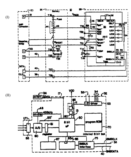
Smart battery l0 of the present invention is
3~ more fully illustrated in Figure 2(a) which is a
simplified block diagram of the smart battery, an
advanced design multi-pin connector, and a battery
module 28 which includes a pinout diagram of the hybrid
CA 02204268 1997-0~-01
J9S114543
WO ~/IS~3
-15-
ASIC 32 used in the present invention. As illustrated
1 in Figure 2(a), the smart battery device 10 includes a
plurality of rechargeable cells generally indicated at
26 which may be Nickel Metal Hydride (NiMH) or Nickel
Cadmium (NiCad) cells.
For the purposes of an illustrative but not -
limiting example, in the following specification, 6 NiMH
cells havin~ a nominal 2400 maH capacity, will be
assumed. Such an arrangement of cells is particularly
appropriate for powering a portable computer.
A suitable advanced design multi-pin battery
connector 30 is used to connect the smart battery to a
host device 16 or power supply 18, as previously
described with respect to Figure 1. The multi-pin
connector 30 includes a positive power supply terminal
31 which is connected to the positive terminal of the
first cell, and a negative power supply terminal 33
which is connected to the negative terminal of the last
cell. A plurality of rechargeable cells may be
connected in series therebetween as illustrated in
Figure 2(a).
The smart battery module 28 includes a hybrid
IC 32 containing a microprocessor 50 (Figure 2(b)) and a
plurality of sensor means for generating analog signals
representative of battery voltage, current and
temperature. The module also includes a series of four
(4) LEDS 34 driven by an LED drive circuit 53 and a
switch 35 which may be manually actuated by an end user
to determine the state of charge in the battery even
when the battery module has been removed from the host
device 16. The LEDS 34 may be used to represent a
3~ relative state of charge (SOC) in a logic scheme as
follows: if the state of charge is greater than 75% (or
less than 100%) then all 4 LEDS are illuminated; if the
- SOC is from 50% to 75%, then 3 LEDS are illuminated; if
CA 02204268 1997-0~-01
rcr/ussstl4s43
WO96/15~3
-16-
SOC is from 25% to 50%, then 2 LEDS are illuminated; if
SOC is from 10% to 25%, then 1 LED is illuminated, and
if SOC is less than 10%, a single LED is flashing. As
mentioned above, relative SOC is remaining capacity
relative to last full capacity.
As shown in Figures 2(a) and 2(b), the hybrid
ASIC 32 also includes an external crystal 36 operating
at a fixed frequency which is used as a time base for
integration of battery current over time, and to ensure
stable start up after a prolonged standby period when
power is reapplied to the smart battery 10. The smart
battery of the present invention utilizes two separate
oscillators, a low power RC oscillator 48 formed within
the hybrid IC 32 and used as an operating clock for the
hybrid IC and the A/D converter 60 therein, and, the
external crystal 36. As will be hereinafter described
5 in greater detail, the external crystal 36 is used to
restart the measurement period after each predetermined
interval to provide for accurate measurements and
integration of battery conditions, regardless of battery
temperature, which can adversely affect the accuracy of
the internal oscillator. The frequency value of
external crystal 36 may range from 10kHz to 66 kHz,
preferably at 32 kHz and the frequency value of
oscillator 48 may range from 450 kHz to 460 kHz.
The hybrid IC 32 includes a MIKRON GmbH low
25 cost, high performance, CMOS 8 bit microcontroller (~P)
50 with an advanced RISC architecture. A reduced set of
32 instructions that are all single cycle instructions
(except for program branches which are two cycles), and
a Harvard architecture scheme achieves a high level of
3 performance with minimal power drain. The
microprocessor operates at a clock input anywhere from
DC to 10 MHz with 12 bit wide instructions and 8 bit
wide data path. A free programmable Counter/Timer
CA 02204268 1997-0~-01
WO g6115563 P~ 114543
--1'7--
circuitry is provided as well as a free programmable
l Watchdogtimer. Additionally, the microprocessor is
addressable in direct, indirect, and relative addressing
modes. The microprocessor 50 is commercially available
- from Mikron Gmbh, located at Breslauer Stra~e 1-3, D-
85386, Eching, Germany, and is available in the U.S.A. -
through MICROCHIP Technology, Inc., Chandler, U.S.A.
The hybrid IC 32 also includes a plurality of
analog circuits which are used, in combination with
external analog sensors, to generate digital signals
representative of battery voltage, current and
temperature as will be hereinafter explained.
For example, as shown in Figure 2(a) battery
voltage is obtained from a voltaqe divider circuit which
includes R1 and R2 which are internally switched by a
NMOS transistor within the hybrid IC 32 to provide
voltage measurement during a small portion of each
measurement interval, thereby minimizing current drain
on the battery cells 26.
The measurement of battery temperature is
accomplished with an NTC-thermistor, illustrated as R~
in Figure 2(a), which varies resistance as its
temperature varies. A resistor R3 is connected in
series to form a voltage divider circuit between
V~,(negative analog power supply voltage) V~,(the
temperature voltage input) and V~, which is a reference
voltage applied to the thermistor/resistor string by the
hybrid ASIC 32 at pin V~. The temperature voltage
input is measured at V~ according to the following
formula:
V~ = R3 x V~
R3 + R~l
wherein the NTC1 value may be 10 kohms at 25~ C and
varies with temperature. If desired, a look-up table
with a plurality of temperature values and a plurality
CA 02204268 1997-0~-01
WO96/15~3 PCT~S95/14~3
-l8-
of V~ values may be defined to calculate the battery
temperature, and between these values, the temperature
is linearly interpolated by the microprocessor within IC
32.
The measurement of battery current is measured
through a shunt resistor, illustrated in Figure 2(a) as
R.hUnt, that is connected in series with the battery cells
and negative terminal 33 of cell pack 26. The shunt
resistor is of small value, but may range anywhere from
l mohm to 200 mohms depending on the number of cells and
expected usage of the battery. The voltage drop across
the shunt is sensed between Vs~, the shunt resistor
positive input pin of ASIC 32, and V~, the negative
analog power supply voltage.
As shown in Figure 2(b), whenever the analog
signals representing battery voltage, current, and
15 temperature are obtained, they are input into an ASIC
multiplexor or switching network 55 which enables only
one analog signal at a time to be input to the A/D
converter 60 for digital conversion. The switching
network acts in conjunction with digital logic circuitry
for informing the A/D converter, via line 55', shown in
Figure 2(b), of the amount of integration cycles to
perform depending upon the type of measurement to be
converted. For instance, more integration cycles are
needed when making a current measurement conversion to
25 ensure a higher bit resolution as compared to when a
voltage or temperature measurement is being converted,
as will be explained in further detail below with
respect to Figure 8(a).
A general schematic diagram of the A/D
3~ converter 60 is shown in Figure 4. In the preferred
embodiment, the A/D converter 60 is a bipolar, high
resolution, incremental sigma-delta converter and
consists of three parts: a bandgap reference circuit 62
CA 02204268 1997-0~-01
WO ~/15~3 PCT~S95/14~3
--19--
which provides a preset analog voltage which is used as
an analog ground for the A/D; a voltage divider network
64 which divides the present voltage to the analog
voltages which are used as the full-scale voltage for
the A/D; and, a sigma delta circuit 66 for converting
the analog signal to a digital word output at line 69. --
A/D control circuit 68 having a clock input from the IC
oscillator, provides the control for the sigma delta
converter which has a different degree of resolution
depending on the type of measurement. For instance, in
one embodiment of the invention, the A/D converter was
configured as having a resolution of 13 bits and a
conversion time ranging from 300 to 400 msec for current
measurements, and, was configured as having a resolution
of lO bits and a conversion time ranging from 30 to 60
msec for voltage and temperature measurements. The
5 timing diagram for the voltage, current, and temperature
measurements in each operating cycle is illustrated as
58a in the timing of operating cycles diagram of Figure
8(a), as explained below.
In one embodiment of the invention, the
20 voltage divider circuit 64 of the A/D converter divides
the preset bandgap reference voltage into the following
full scale voltages: a 150 mV signal used as the full
scale voltage for the battery current measurement; l50
mV, 250 mV, or 350 mV signals used as the full-scale
25 voltage for the battery pack voltage measurement and
dependent upon the number of battery cells; and 150 mV
used as the full-scale voltage for the battery
temperature measurement. These values are illustrative
and may vary as battery design varies.
3 The A/D converter of the smart battery device
utilizes a sigma-delta converter circuit 66 as explained
above in view of Figures 4 and 6. Details of the sigma-
delta converter circuit 66 capable of bipolar conversion
~ 35
CA 02204268 1997-0~-01
Wo9611S~3 PCT~S95/14~3
-20-
are explained hereinbelow in view of Figures 5(a),5(b)
and Figures 6 and 7. Figure 6 particularly illustrates
a switching capacitor network for receiving positive and
negative voltage values, indicated as V~N in Figure 6 for -
input into an integrator circuit 88 and comparator
circuit 89 for output into control and logic circuit 68. '
In the reference, Jacques Robert et al., (1987) "A 16-
bit Low-Voltage CMOS A/D Converter", IEEE Journal of
Solid-State Circuits, Vol. sc-22, No. 2, 157-159, an
incremental (integrating) sigma-delta converter
implementing 4-~m CMOS, switched capacitor technology
similar to that implemented in the A/D converter of the
smart battery device is disclosed. What is described in
the reference is a simplified, unipolar A/D converter
that is largely insensitive to variations in clock
frequency and clock waveforms due to the fact that all
5 signals are represented by charges, rather than
currents, as in the switched capacitor integrator that
forms the core of the converter.
In the prior art, to measure positive and
negative input voltages, a negative power supply is
20 necessary in addition to the positive voltage supply.
Thus, where it is desired to measure negative voltages
(or currents) such as smart battery discharging current,
external components (such as inverters) and circuitry
that consume extra power are required, and the prospect
25 of utilizing such circuitry for the low power
application such as needed in the smart battery device
of the instant invention, is diminished. Instead, to
overcome this drawback, the A/D converter 60 of the
instant invention does not utilize a negative voltage
3~ power supply, but makes use of an available on-chip A/D
bandgap reference voltage "AGND" to be used as a virtual
ground. The concept of utilizing a "virtual ground" is
based on the fact that a voltage stored on a capacitor
CA 02204268 1997-0~-01
WO ~/1S~3 PCT~S95/14~3
-21-
can be transferred to another d.c. voltage reference
point using analog switches with virtually no loss of
charge.
In Figure 5(a) there is represented a first
embodiment of the dc voltage shifting circuit
arrangement, consisting of three switches Sl through S3,
and four connectors Al through A4 and a capacitor Cl
(with the capacitance Cl). The connectors Al, through
respectively A4 are at the potentials ~1 through
respectively ~4. As shown in Figure 5(a), the switch Sl,
and the combination of parallel-connected switches S2
and S3 are connected to opposite terminals of the
capacitor Cl.
In the following there is described the
operation of the inventive circuit arrangement. At the
beginning, the switches Sl and S2 are closed and the
15 switch S3 is open. The capacitor charges itself up due
to the voltage differential ~ 2 and stores a charge Cl
X (~ 2)-
In the next step of the inventive process, the
switches Sl and S2 are opened and one pole of the
20 capacitor is connected through switch S3 with a
potential ~3. Present at the capacitor Cl is now a
voltage ~3 + ( ~ 2 ) which can be tapped off through
connection with the connectors A3 and A4 which lie on
the potentials ~3 and ~4.
In Figure 5(b) there is now represented a
further embodiment of the dc voltage shifting circuit
whereby an additional switch S4 is provided which, when
open, prevents the presence of a potential ~1 at the
tapping off of the voltage ~3 + (~ 2) present at the
3~ connectors A3 and A4, when switch Sl is closed.
In Figure 6 there is illustrated the schematic
circuit diagram of the inventive circuit arrangement in
a switched capacitor A/D converter. The A/D converter
3~
CA 02204268 1997-0~-01
PCT~S95114~3
W096/15~3
-22-
66 possesses an operational amplifier 88 which is
utilized as an integrator, and an operational amplifier
89 which is utilized as a comparator. The non-inverted
input of the comparator 89 by means of the line 9l
stands in connection with the output of the integrator
88. The inverted input of the comparator 89 and the
non-inverted input of the integrator 88, are connected
with a reference potential AGND, (analog ground = 1.25
volt). The output of the comparator 89 is "high", in
the event that the output voltage of the integrator 88
is higher than the reference voltage AGND and "low" in
the event that the output voltage of the integrator 88
is lower than the reference voltaqe AGND. By means of
the lines Ll, L2, L3 and L4, the integrator 88 or, in
essence, the inverted input and the output of integrator
88 have connected in parallel therewith a capacitor C2
5 with a capacitance C2. The capacitor C2 has a switch SR
connected in parallel therewith through lines Ll and L5,
which can effectuate a discharge of the capacitor C2.
Through a line L6, the inverted input of the integrator
88 stands in connection, by means of a switch S5 and a
20 line L7, with a capacitor Cl having the capacitance Cl.
A line L8 connects the line L7 through a switch SI and
the line L4 with the output of the integrator 88. The
line L9 connects the pole of the capacitor Cl facing
towards the integrator 88 in Figure 6 with a line LlO,
25 which stands in connection through the line Lll, Ll2 and
respectively Ll3, with the switches S4, S7 and,
respectively S6. Connected to the other pole of the
capacitor Cl is a line Ll4, which is connected through
the switch S3 with the reference voltage AGND = l.25
3 volt. A line Ll5 stands in connection with line Ll4 and
connects through the lines Ll6, Ll7, and respectively
Ll8, the pole of the capacitor Cl, which faces away from
the integrator 88 in Figure 6, with the switches S2, Sl,
CA 02204268 1997-0~-01
PCT~S95/14~3
WO96/lS~
-23-
and respectively, S8. The internal mass of the chips V.
~ 0 volt stands through the line Ll9 and, respectively,
- L20, in connection with the switches S8, respectively,
S6. In this matter, through suitable opening and
-~ closing of the switches S8 and S6, the voltage V... can be
applied to both poles of the capacitor Cl. The input
voltage VIN which is to be digitized stands in
connection with the switches Sl and, respectively, S7,
through lines L21 and, respectively, L22. In this
manner, through suitable opening and closing of the
switches Sl and S7, the input voltage V~N can be applied
to either of the two poles of the capacitor Cl. The
reference voltage V~F which determines the resolution
of the A/D converter is connected through lines L23 and,
respectively, L24 with the switch S2 and, respectively,
S4. In this manner, the reference voltage V~F~ which,
for example, consists of 150 milli- volt, can be applied
to one of the two poles of the capacitor Cl. The
switches Sl,....,S8, SR and SI are preferably CMOS
switches, especially CMOS transmission gates. The
connection of the input voltage VIN~ the reference
20 voltage V~F and the mass V.~ with the input capacitor Cl
of the A/D converter is known in the technology.
Inventively there is connected through the switch S3 a
reference voltage AGND =1.25 volt (~VBS = 0 volt) to the
input capacitor Cl. Similarly, through the inventive
25 circuit there is facilitated that VIN/ V~F and AGND can
be applied to both sides of the input capacitor Cl,
which presently causes a charging up at different
polarity of the capacitor Cl.
In Figure 7, there is illustrated the
3~ operation of the A/D converter in a phase diagram.
Thereby, Sl through S8, SR and SI designate the switches
of the A/D converter 66 pursuant to Figure 6, and CK is
CA 02204268 1997-0~-01
9S114543
WO96tlS~3
-24-
the pulse signal of the comparator 89 in Figure 7. CK'
represents a further tapped-off pulse signal.
In the diagram, the switch conditions
fluctuate between 0 and 1, whereby 1 signifies that the
switch is closed, whereas 0 stands for the opened
switch. The operation of the A/D converter can be
divided into four phases which are designated with I,
II, III and IV whereby I designates a RESET or resetting
phase; II an integration phase, III and inverting phase
and IV an integration phase of the input voltage of
reverse polarity or sign. The cycle is more finely
subdivided into steps i, --- xiv. As shown as step i in
Figure 7, during the reset phase I, only the switch SR
is closed, whereas all other switches are opened. This
causes a discharge of the capacitor C2. At the
beginning of phase II, as indicated as step ii, in
Figure 7 the switches S1 and S6 are closed, whereas all
remaining switches remain further open. This causes a
charging up of the capacitor to a charge ~Q=Cl x (VIN ~
V..)=C1 X VI~. In step iii, the switches S3 and S5 are
closed, whereas all other switches remain open. One
20 pole of the capacitor is now set to the potential AGND,
whereas the other pole of the capacitor C1, through
closing of the switch S5, stands in connection with the
capacitor C2. There now takes place a charge transfer
from the capacitor C1 to the capacitor C2. Inasmuch as
5 the integrator of 88 resultingly causes the two input
potentials to be equalized, there is present at the
output 91 of the integrator 88 the output voltage VO~
equal - (C1/C2) x VIN + AGND. In step iv all switches
are opened and the comparator pulse CK is 1, meaning,
3 the comparator 89 carries out a comparison between VO~
and AGND. Upon the result of this comparison there now
depends the further cycle. The representation of the
switch conditions in step v must be understood in the
CA 02204268 1997-0~-01
PCT~S95/14~3
WO ~llS~
-25-
following manner: In step v the switches S2 through S8
are not closed, but the switches S2 and S6 are closed,
- and Sl, S3, S4, S5, S7, SR and SI are open, in the event
that the output of the comparator is 0, in effect "low",
while the switches S4 and S8 are closed and Sl, S2, S3,
S5, S6, S7, SR and SI are open when the output of the
5 comparator is l, meaning, "high", and in other instances
remain open. When the output of the comparator is 0,
meaning the output voltage V0~ is lower than AGND, then
the switches S2 and S6 are closed. At the capacitor Cl
there are now present VR~ and VSs. In the instance in
which the output of the comparator is l, meaning, V0~ is
higher than AGND, then the switches S4 and S8 are
closed, whereby similarly Vn8 and V~ are present at the
two poles of the capacitor Cl, but with the reverse sign
or polarity than in the instance in which the output of
5 the comparator is 0. In step v, the switches Sl, SR and
SI are opened, and in step vi, the switches S3 and S5
are closed (compare step iii) which causes that the
capacitor Cl and C2 to be interconnected. As in step
iii, voltage AGND is applied to one pole of the
20 capacitor Cl. There again, in turn takes place a charge
transfer between the capacitors Cl and C2, as result of
which a voltage - (Cl/C2) x V~ + AGND is added to or,
respectively, subtracted from that of the output voltage
of the integrator 88, in accordance with the result of
25 the comparison by the comparator in step iv. During the
steps i through vi of phase II there is processed an
input voltage which is phase shifted with respect to
AGND, with a reference voltaqe which is shifted relative
to AGND. Similarly, at the non-inverted input of the
3~ integrator 88 and the inverted input of the comparator
89 there lies AGND, which causes that the output voltage
is referenced to AGND and causes a comparison by the
CA 02204268 1997-0~-01
PCT~S95/14~3
W096/lS563
-26-
comparator 89 not with V.~ = 0 voltage, but with AGND =
l.25 volt.
In the following there is now discussed phase
III consisting of steps vii to ix. In this phase, a
sign or polarity reversal is implemented for the output
voltage Vo~ of the integrator 88 with reference to AGND. ~-
During the entire phase III the switch S3 is closed.
The closure of the switch S3 during the phase III causes
the voltage AGND to be applied to one pole of the
capacitor Cl, as a result of which the voltage V0~ is
also inverted with regard to AGND and not with regard to
V.. = 0, as in the known A/D converters. In step vii
there is now closed the switch SI, whereas all remaining
switches are open, except swltch 53. This causes that
the voltage Vo~ is temporarily in the capacitor Cl, such
that in step viii all switches are opened except switch
5 SR. The switch SR is in effect closed, which causes a
discharge of the capacitor C2. In the step ix the
switch S5 is closed additionally to switch S3, while all
remaining switches are opened. This causes that the
negative voltage which is phase shifted at AGND is
20 present at the output of the integrator 88. The
negative sign is obtained, as previously through the
charge transfer from the capacitor Cl to the capacitor
C2. In step x of Phase IV, the switches S7 and S8 are
closed, whereas all remaining switches are opened.
25 Compared with the step ii the input voltage VIN is
present with a reverse polarity at the capacitor Cl.
This causes a change in the sign of the integration of
the input voltage, which is also well recognizable in
Figure 6 of the above mentioned publication of Jacques
3 Robert et al. The steps xi through xiv correspond with
the steps iii through vi, meaning, there is implemented
an integration of the input voltage (only due to step x
with a reverse sign of VIN), and in accordance with the
CA 02204268 1997-0~-01
PCT~S9~/14~3
W096/lS563
-27-
result from the comparator 89 in step xii VR~ is added
1 or, respectively, subtracted after the integration (in
case C1 = C2). For a 14-bit A/D-converter, after
implementing of step i there is carried out phase II
[21~-2 (for the phases I, and III)]:2 = 8191 times), as
well as phase IV. The output of the comparator is ~-
connected to a up/down counter, which each time, in
accordance as to whether V~ is added or subtracted,
increases or lowers its count condition by 1. The
result of the counter is then a 14-bit representation of
the ratio of V~N to VR~. The phases III and IV are
necessary since through the integration with reverse
signs of V~N offset errors encountered in, for example
the operational amplifiers, are reported or,
respectively eliminated.
The multi-pin connector 30 includes two pins
5 for the system management bus interface 75, which
include a serial clock I/O line 38 and a bidirectional
serial data I/O line 40. These lines are connected to
the SMBCLK and SMBD data pins, respectively, of the
hybrid IC 32. As explained generally above, and, in
greater detail below, the smart battery module 28
communicates with the host device 16 and the smart
charger 22 over the system management bus and data line
40 to communicate both stored battery parameters and
calculated battery parameters.
The smart battery 10 also includes a separate
thermistor R~2 which is connected across the negative
terminal of multi-pin connector 30 and a temperature or
thermistor line 42. Thermistor R~2 may be used
independently by the smart charger 22 to determine
3~ battery temperature, in a manner similar to that
previously described with respect to R~l.
A positive digital power supply voltage is
obtained from the plurality of rechargeable battery
CA 02204268 1997-0~-01
PCT~S9S/14~3
WO ~/15~3
-28-
cells 44, and supplied to the hybrid IC through pin VDD
as the positive power supply voltage for the chip. It
should be understood that the supply voltage for the
hybrid IC does not necessarily have to be obtained at
the battery midpoint 46, but should be obtained at a
point from the battery cells in order to receive a --
voltage of approximately 3 to 4.8 volts, i.e., the
equivalent voltage of three (3) cells. As will be
hereinafter explained in greater detail, the use of a
battery midpoint for the positive voltage supply enables
the hybrid IC to remain powered even when the battery is
accidently shorted and removed from terminals 31-33, and
enables the A/D converter 60 to determine whether the
battery is discharging or being charged as will
hereinafter be explained in greater detail. Suitable
fuse elements (one of which is shown in Figure 2(a)),
5 and a positive temperature coefficient (PTC) elements
(one of which is shown in Figure 2(a), are provided in
series with the battery pack cells to protect the
battery from very high current and excessive
temperatures caused by a temporary short circuit across
the battery terminals or other thermal event.
As shown in Figure 2(b), the hybrid IC 32
further includes RAM memory 65 which can store up to 128
8-bit registers for communication of calculated battery
parameters, and a ROM memory 67 for storing look-up
5 table values utilized in the battery capacity
calculation algorithm (explained in detail below). The
exact amount of RAM, ROM, and program ROM memory is a
design choice, and these values change as the ratio
between calculated and preset parameters vary.
3 As shown in Figure 2(a), the addition of
capacitor C4 acts as a buffer to maintain the integrity
of the RAM memory contents in the case of a battery
short-circuit or temporary power loss. Preferably, the
CA 02204268 1997-0~-01
WO 96~1S563 ~ J9SI14543
--29--
capacitor C4 is connected to the negative analog voltage
supply terminal, and its value is chosen to ensure that
~ a source of supply voltage is supplied to the embedded
memory (RAM) for a time dependent upon the RAM leakage
current. In the preferred embodiment, the power to RAM
memory is unlatched if a temporary short circuit
condition exists, However, capacitor C4 preferably of
capacity 330 nF, provides a source voltage to the RAM
for a period of time necessary for the PTC element to
ramp to a high resistance value. The PTC element will
create a high impedance between battery terminals when a
short circuit across the battery pack terminals creates
a high circuit drain.
The hybrid IC 32 further includes up to 4
kbytes of additional ROM memory 70 for addressing and
storing the various algorithms, subroutines,
manufacturer data, and data constants utilized by the
smart battery module for calculating the battery
capacity, sending messages such as alarms and battery
charger control commands etc., and handling message
requests from external devices.
The programmable ROM generator is implemented by
means of a metal mask (not shown) as opposed to
conventional ROM generation by means of diffusion
masking. In accordance with the information which was
to be permanently stored, transistors were generated in
25 a matrix arrangement through diffusion, whereby the
information was coded in the plane through the
distribution of the transistors in the diffusion step.
Thus, the ROM generator generates in effect, a ROM
matrix, whereby the presence or respective absence of an
3 MOS transistor stands for a logic "O" respectively "1."
A disadvantage of a ROM matrix with the programmable
level of diffusion is that the diffusion process, which
is incorporated as one of the first steps of a CMOS
CA 02204268 1997-0~-01
PCT~S95114~3
W096/15~3
-30-
process, can not be changed when there is a change in
ROM contents, thus, rendering impossible the production
of wafer stock for a particular type of ROM.
By contrast, the advantage of a ROM matrix
programmable in a metal layer is that wafer stock with
the same basic layers up to the metal may be fabricated.
Thus, a microprocessor family with different ROM
contents can be realized with low cost and fast turn
around time. Additionally, the pre-manufacture of a
portion of the ROM with the flexibility of programming
in application specific information in the upper or
respectively later produced layers, is possible.
The hybrid IC chip itself may comprise
thirteen or fourteen layers, with the gth or 10th layer
(i.e. one of the upper layers) being a layer of metal,
wherein the distribution of the metal is characteristic
5 for the storing contents of the ROM. Thus, in the
hybrid IC ROM manufacturing process, nine (9) layers are
grown and the next four ROM programming layers are grown
dependent upon the customer's particular needs (i.e.,
special properties of the battery pac~).
Figure 9(a) shows a ROM matrix with the metal
layer as a programmable layer. A MOS transistor, e.g.
71(a) for the matrix is always present on the matrix and
will either serve as a logical "0" or "1".
Specifically, Figure 9(a) schematically illustrates the
25 ROM 67 of the smart battery device that is programmed
according to the unique process as follows: The
represented ROM matrix consists of eight word lines 67a
and indicated as WZO, ..., WZ7 and 8 spaces 67b and
indicated as SPO, ..., SP8, whereby the spaces
3 SPl,SP3,SP5,SP7 connect with a virtual ground line 73.
At each location of the matrix, there is produced a
transistor in the diffusion step, three transistors 71a,
71b, and 87 of the matrix are shown in Figure 9(a). For
CA 02204268 1997-0~-01
W096/lS~3 PCT~S95/14~3
-31-
the programming of a logic "0," in a respective word
l line, the drain or respective source electrodes of a
- transistor are connected to a metal mask with the
corresponding source or respectively drain electrodes of
the joining transistors or the joining transistor. The
5 drain or respective source electrodes of such a
transistor are connected with the gap lines or,
respectively, the virtual ground lines 73. Transistor
71a in word WZ7, as shown in Figure 9(a), is programmed
for a logic "O" as its drain terminal is connected with
the source terminal of connecting MOS Transistor 87
which is tied to virtual ground line SP7.
Logic "1" in contrast therewith is probed in,
in that the drain or respectively source electrodes are
connected to a common line, preferably, as can be
ascertained from Figure 9(a), to a gap line
5 SP0,SP2,SP4,SP6,SP8. Thereby, the transistors, such as
the transistor 71b of word WZ0 as shown in Figure 9(a),
are short circuited.
The connections of the transistors are thus
initially determined with the application of the metal
mask. In the usual manner two (through contacting)
metal masks are applied on the ROM. In should be
understood that in this instance preferably the lower of
the two metal masks, meaning the mask which is located
closer to the transistors, is employed for the short
25 circuiting and the connection of the applicable
transistors. Inasmuch as the transistors are short
circuited, this does not influence the operation of the
metal mask which is employed for the contacting. Since
this metal mask is usually one of the uppermost layers,
3~ for example the tenth of about 14 layers, the inventive
ROM can be pre-manufactured up to the ninth layer and
then programmed and manufactured in accordance with the
application.
CA 02204268 1997-0~-01
WO96/1S~3 PCT~S95/14~3
-32-
In Figure 9(b) there is illustrated a usual
1 programmed ROM. It can be ascertained from Figure 9(b)
that the transistors, which are short circuited in
Figure 9(a), are in any event not produced in the
diffusion mask. As shown in Figure 9(b), the transistor
71c which is not present corresponds to a short ~~
circuited transistor 7lb in the metal mask pursuant to
the process described above.
Each of the algorithms, subroutines,
manufacturer data, and data constants stored in ROM and
utilized by the smart battery module for calculating the
battery capacity, etc. as mentioned above, will now be
explained in further detail below. Further details of
the smart battery algorithm for reporting battery
parameters to an external device is found in applicant's
co-pending patent application U.S. Serial No. 08/318,004
assigned to the assignee of the instant invention and
the disclosure of which is incorporated by reference
herein.
As shown in Figure 3, the battery operating
system 10' will first perform an initialization routine
100 that is initiated upon system power up, enabled by a
power ON signal/reset impulse signal 11, or, enabled by
a wakeup from STANDBY signal 13 which is generated after
the microprocessor has determined that it should exit
the standby mode. As shown in Figures 2(b) and Figure
5 10, the hybrid IC 32 is provided with a power-on reset
circuit 85 which generates a reset impulse signal 11 to
activate the external crystal oscillator 36 and reset
the system every time the power supply voltage is
applied to the ASIC. Specifically, this reset impulse
3 initiates the start of the external crystal oscillator
36 to provide the precise triggering of the internal 450
kHz oscillator for providing the time base for the
hybrid IC components. The threshold of this circuit is
CA 02204268 1997-0~-01
WO 96/1SS63 P~ 9!;/14543
--33--
between 1.2 V and 1.6 V depending upon the type of
1 transistors used in the circuit of Figure 10.
~ More specifically, as illustrated in Figure
10, the power-on reset circuit 85 is provided with a
transistor network comprising n- and p- channel
transistors that are tied to hybrid IC voltage supply
VDD. When VDD is sensed as dropping between 1.6V to 2.0V,
or, in the case of battery short circuit 0.0 V, the
transistors of circuit 85 generate a RAM memory de-
latching signal 79 which turns off PMOS- transistor 85'
and effectively de-latches RAM memory 65. As mentioned
above, the voltage on buffer capacitor C4 will keep RAM
memory contents alive for period dependant upon RAM
leakage current.
After a power on/reset signal 11 is received,
or, after the sleep mode is exited, the system is placed
5 in a standby mode 23 (Figure 3) until it is triggered by
trigger signal 17 generated by the external oscillator
36 which provides the trigger for the system operations
(capacity calculation) every 500 msec, or, is awakened
by a bus request signal 15 as will be explained in
further detail below. In the battery "standby" mode,
the microprocessor is in an idle state until the
operating cycle trigger 17 or external bus request
signal 15 is received.
25 Initialization of algorithm variables
The initialization routine, which is described
and shown (in Figure 4) of the above-mentioned, co-
pending patent application (USSN 08/318,004), is
3~ conducted at the virginal start of the system. The
initialization routine functions to clear all values to
be stored in the system RAM and to assign all system
default values. Preferably, many of the default values
CA 02204268 1997-0~-01
PCT~S95/14~3
W096/lS563
-34-
are constant values and are available in case of an
emergency situation wherein all RAM memory has been lost
while the system was in the STANDBY mode.
On power-on-reset as well as on a wakeup from
the STANDBY mode of the chip (explained below), the
program is started at an initial memory address. A
"checksum" test is conducted for checking whether the
RAM memory is valid whereby the capacity calculation is
continued, or, whether the emergency mode (which uses
ROM defaults) will be activated. Such an instance
occurs when the chip switches into the STANDBY mode at
low battery voltage and then back into the ON mode when
the battery is to be recharged.
If the "checksum" test fails, the yP will
first clear all RAM banks completely, and, as
consequence an internally generated CALIBRATED flag will
5 be cleared and the number of cells of the battery pack
has to be learned, a process to be explained in greater
detail below. Next, the default values (described
below) are transferred from ROM to RAM. To prevent
exceptions in the capacity calculations to be described
~ hereinbelow, it is imperative that variables do not have
undefined values. This enables the algorithm to work in
a catastrophic emergency mode in the event that all RAM
memory has been lost. The default values of critical
variables may then be substituted by correct values when
25 the battery system is reformatted at a battery service
station using the original manufacturer's data.
Included in the initialization routine will be
an initialization of FullChargeCapacity "full_cap",
RelativeStateOfCharge "SOC" and the RemainingCapacity
3 "Itf" values, as well as state and other variables to
ensure a proper start of the capacity calculation.
Then, the program resets all system timers such as the
calculation of voltage, temperature and selfdischarge
CA 02204268 1997-05-01
PCT~S95/14~3
WO ~/IS~3
-35-
timers before passing out of the initialization routine.
The capacity calculation will then initiated at each
trigger signal 17 which is delivered every 500 msec by
the external 32 kHz crystal 36.
As explained above, the default values are
necessary to ensure that upon a power-on/ reset, the
rechargeable battery capacity calculation (explained
below) may be executed. The preferable nominal default
values for the critical parameters used for the capacity
calculation algorithm l5l and explained in detail in co-
pending patent application (USSN 08/318,004), are set
forth as follows:
The DesignCapacity (theoretical or nominal
capacity, hereinafter "nom cap") may range between 1700
maH to 2400 mAH, but, after a memory loss, the capacity
calculation algorithm defaults to a preferred value of
5 2000 mAh and the new capacity is relearned from that
level; the default value of the number of battery cells
in the rechargeable battery pack is 6 cells, however,
this value may be changed depending upon the actual
configuration of the battery pack; The AL_REM_CAP value
20 represents the remaining capacity alarm triggering value
and may range from 50 mAh to 500 mAh. Preferably,
AL REM CAP has a default value (AL_REM_CAP DEF) of 200
mAh. An alarm condition exists when the remaining
capacity is below this value (without taking into
25 account the remaining capacity after EDV due to current
and temperature (i.e., the residual capacity
correction)). The AL_REM_TIME value represents the
estimated remaining time at the present discharge rate
and may range from l.0 min. to 20 min.. Preferably,
3 AL REM TIME has a default value (AL_REM_TIME_DEF) of lO
minutes. This alarm condition exists while the
calculated remaining time to voltage breakdown (EDV),
based on the minute average current (discussed below),
CA 02204268 1997-0~-01
W096/lS~3 PCT~S95/14~3
-36-
is below the value of AL_~EM TIME and will automatically
1 be disabled when the battery is in the charging mode.
The AL_DTEMP value represents the dT/dt alarm trigger
condition and may range from 1~K/min. to 5~K/min..
Preferably, AL_DTEMP has a default value (AL_DTEMP_DEF)
5 of 2~K/minute. This alarm condition will exist when the
battery detects that the rate of its internal thermal
rise (dT/dt) is greater than the AL_DTEMP value. The
AL_HI_TEMP value represents the high temperature alarm
trigger and may range from 310~K to 345~K. Preferably,
AL_HI_TEMP has a default value (AL_HI TEMP_DEF) of
328~K. Additionally, when the capacity calculation is
started by power-on-reset, the FullChargeCapacity,
("full_cap" represents the learned full charge capacity
of the battery), will be initialized to the
DesignCapacity (nom_cap); the RemainingCapacity (~'Itf")
to 1/8 of the full_cap; and, the RelativeStateOfCharge
("soc") to 12.S% and the battery state to capacity
decreasing, and, specifically, to selfdischarging mode.
The alarm timer N_ALARM is set at 10 seconds and this is
the amount of time that an alarm condition will be
broadcast between a host device and/or a battery charger
as will be explained in further detail below. It should
be understood that these values are typical values for a
NiMH battery intended for use in a portable computer.
Other types of battery chemistry, or portable devices,
5 may call for a different set of default values.
As shown in Figure 3, after the system is
initialized at step 100, the battery will enter into a
standby or maintenance mode 23 where it will either
awake upon a bus-request signal 15 or awake upon the
3 external crystal trigger signal 17 every 500 msec. If
the battery is awaked by a bus request signal 15 as
determined at step 21, then the battery will handle the
request by the handle request routine indicated at step
CA 02204268 1997-0~-01
wOs6/15~3 PCT~S95/14~3
-37-
25 where it will thereafter exit into the standby mode.
The routine for handling the requests 25 will be
~ explained in further detail below.
If the system is triggered by the normal
external crystal trigger signal 17, and there are no bus
requests, then the program disables the bus requests -~
5 (approximately 37 msec before the trigger signal) and
enables the A/D converter to begin the current, voltage,
and temperature measurements for the current operating
cycle as shown at step 130 in Figure 3. A "getvalues"
status flag is then checked at step 139 to determine
whether A/D conversions of the raw current, voltage, and
temperature measurement values are to be performed.
When this flag is set high (logic level =1), the raw
current, voltage, and temperature values of the
rechargeable battery are obtained for the current
5 trigger cycle as shown at step 140. These raw A/D
current, voltage and temperature values are built into a
special function register 61, as shown in Figure 2(b),
which is one of sixteen such registers provided in the
hybrid IC for subsequent storage in RAM as I, U, or T.
2 If the "getvalues" flag is low (logic level =0), then no
raw current, voltage, and temperature measurements will
be obtained for the present cycle, and the getvalues
flag will toggle high (logic 1) at step 148 and the
process will continue as shown in Figure 3.
After new current, voltage, and temperature
values are obtained (step 140), the A/D measurements
ready flag is set high (logic level =1) at step 141, and
a check is made at step 142 to determine whether the
system is in a sample mode. Thus, at step 142, if the
3 absolute value of the raw current, tII, is determined to
be below a threshold value of 10 mA, then the battery
system will operate at half the sample rate depending
upon the status of the sample mode flag. Thus, at step
CA 02204268 1997-0~-01
WO 96/1Ss63 PCI'lUSgS114543
--38--
143 in Figure 3, a determination is made as to whether
l the sample mode flag is low (i.e., logic 0) or high
~logic 1). If the sample mode flag is low, then the
sample mode flag will toggle to a high level at step
144, and the system is placed in a sample mode and the
5 process proceeds at step 149 to initiate the A/D
conversion. If the sample mode flag is already high
(from the previous cycle), then the "getvalues" flag is
set equal to zero at step 146, and the A/D converter is
disabled at step 147. The A/D conversion will not occur
(to save power) and the algorithm proceeds to the
capacity calculation (step 151). The "getvalues" flag
is always set low in the sample mode. The status of
this flag ensures that an A/D conversion will be
skipped, and, as a consequence, no new valid data will
be available for the capacity calculation at step 150.
- If the raw current, III, is determined at step
142 to be above the 10 mA threshold, then the battery
system will exit the sample mode (and the sample mode
flag is set at logic 0) at step 145, and the A/D
conversion of the raw current, voltage, and temperature
values will be performed at step 149. At step 150, a
determination is made as to whether the A/D measurement
ready flag is high (logic 1) indicating that valid raw
battery parameter data has been received. If it is set
high, then the capacity calculation and attendant
battery characteristic conversions (voltage, current,
and temperature) will be performed. If the A/D
measurement ready flag is low (logic 0), then the
capacity calculation is not performed in the current
cycle, and the process proceeds to step 158 where the
3 bus request line for message transfer is enabled and the
hybrid IC is placed in the sleep mode at step 23. The
oscillator trigger 17 continues to wake up the
microprocessor every 500 msec, however, when the current
CA 02204268 1997-0~-01
WO96/1S~3 PCT~S95/14~3
-39-
is less than 10 mA, the A/D conversions and the capacity
calculations may be performed at an arbitrarily
- determined rate that is less frequent, for e.g., once
every two or once every five seconds, to conserve power.
Figure 8(a) illustrates the timing of the
5 operating cycles under normal mode operating conditions
57a as compared when the system operates under sample
mode conditions 57b explained below. As shown in Figure
8(a) and, as mentioned above, the 32 kHz external
crystal delivers the trigger signal 17 every 500 msec to
initiate the raw voltage, current, and temperature
measurements, indicated as 158. Also initiated is the
capacity calculation 160 which utilizes the current,
voltage, and temperature measurements of the previous
operating cycle. When the raw current value obtained is
determined to be below a threshold value of 10 mA, the
5 battery system will operate at half power, and no
measurements will be taken during the next 500 msec
operating cycle as indicated as 58b in Figure 8(a).
However, measurements are taken one second later at the
next operating cycle as indicated as 58c. When the raw
current value obtained is determined to be above a
threshold value of 10 mA, the battery system will resume
normal mode operation and during the next and subsequent
operating cycles, the capacity calculation and attendant
battery characteristic measurements (voltage, current,
25 and temperature) will be taken.
Figure 8(b) illustrates the approximate time
durations for the various measurements. As a matter of
design choice, the capacity calculation 160 is performed
in approximately 71 msec for each operating cycle.
3~ Thereafter, the alarm control subroutine 152 will be
performed for a duration of approximately 29 msec and
the charger control subroutine 154 will be performed for
a duration of approximately 2 msec if the smart battery
CA 02204268 1997-0~-01
W096/1S563 PCrlUS95/14543
--40--
determines these operations are to be performed (see
Figure 3). The LED display routine 156 may be performed
if it is requested by a user and the LED display control
functions will take place for approximately 23 msec as
shown in Figure 8(b). It should be understood that the
5 aforementioned performance times for the various
routines may vary due to the accuracy of the internal
455 kHz oscillator, which may vary with temperature.
Each of the alarm control subroutine 152, charger
control subroutine 154 and LED display subroutine 156
will be explained in further detail below.
Since the system management bus request line
is inactive during the capacity calculation, alarm
control, charger control, and LED display routines, the
microprocessor will be unable to receive requests from a
host device or battery charger as indicated for the time
5 duration 158 for each operating cycle shown in Figure
8(a). Therefore, in each operating cycle, after the
capacity calculation has been performed, the System
management bus request line is enabled for the remaining
time of the 500 ms cycle, as indicated in Figure 8(b),
so that it may respond to a request from a host device
or charger. Concurrently, the battery places itself in
the standby mode 23 whereupon it will be awaked for the
next cycle upon receipt of the system trigger signal 17,
or, be awakened by a bus request signal 15 as shown in
5 Figure 3. For a remaining 37 msec of each operating
cycle, the bus request is again disabled as shown for
the time duration 158 prior to the next trigger signal
17. As mentioned above, each system trigger signal 17
initiates the start of the internal clock 48 generating
3 the 455 kHz signal for controlling the hybrid IC,
microprocessor, A/D converter, etc.
CA 02204268 1997-0~-01
WO 96/lSS63 rCI'lUS95114543
--4 1--
Alqorithm for calculatinq battery capacity
' The purpose of the capacity calculation is to
continuously monitor the capacity of the rechargeable
battery in accordance to the formula indicated by
equation (1) as follows:
CAPr~ = CAPr~ + ~cIc~tc - ~Id~td - rI,~t. ( 1 )
where CAPr~, is referred to hereinbelow as "Itf" and
indicates the remaining capacity in the battery at any
given time expressed as mAh (milliamperehours); the
~gIC~tc term represents the sum of the incremental
increases in capacity as the battery is being charged
and takes into account a charge efficiency factor
accessed preferably from look-up table values to be
explained in further detail below with respect to Figure
22(c), or, alternatively, may be obtained from a
response equation or by interpolating between several
points stored in memory; a ~Id~td term which represents
the sum of the continuous decrease in battery capacity
due to discharge associated with the battery's usage;
and a ~ t, term which represents the predicted and
measurable amount of self-discharge based upon self-
discharging effects associated with the battery's
chemistry and is a function of the battery state of
25 charge and temperature. By knowing the
RemainingCapacity, Itf, at all times, it is possible to
provide battery parameter information useable by a host
computer (PC) or smart battery charger to ensure safe
and reliable battery use and to ensure prolonged battery
3~ life.
Figures 13(a) through 13(b) illustrate the
capacity calculation routine performed for the
rechargeable battery pack at each trigger cycle. In
CA 02204268 1997-0~-01
WO ~/lS~3 PCT~S95/14~3
-42-
parallel, the current, voltage and temperature
1 measurements are running except when in the "sample"
mode where these measurements are taken once every
second. The sample mode is designed to save power
consumption (i.e., the A/D conversions occur at half-
5 frequency) and is switched on and off depending upon theamount of detected current. For example, when the
current falls below 10 mA, the "sample" mode is enabled
and less frequent measurements are made.
- Normally the temperature, voltage and current
lO are measured and updated once per cycle. The current is
measured with an integrating method (explained in detail
below), which recognizes its changes during the
conversion time. All output values taken from SMBus
requests and capacity calculation are one period
delayed. The A/D measurements are controlled by an on-
5 chip oscillator at nominal 455 kHz and the operating
cycles - responsible for the integration time - by the
precise 32 kHz oscillator. The lower accuracy of the
absolute frequency value of the on-chip oscillator has
no influence on the accuracy of the measurement.
As shown in Figure 13(a), step 200, the first
step of the capacity calculation, the IUT Calculation
routine 200 is performed to first convert the raw
analog/digital converter output data from register 61
(Figure 2(b)) into values having appropriate units
useful for the capacity calculation algorithm. Details
of the IUT Calculation routine can be found in the
above-mentioned, co-pending patent application (USSN
08/318,004). Briefly, as illustrated in Figure 12, at
step 205, the raw A/D Current measurement, I_raw, is
3 scaled and converted to the actual current value "I" in
units of milliamps. Similarly, the raw A/D pack voltage
measurement, U_raw, is scaled and converted to the
actual battery pack voltage value "U" in units of
CA 02204268 1997-0~-01
WO ~/15~3 PCT~S95/14~3
-43-
millivolts. Next, as indicated at step 212, the ~P
1 checks the battery pack voltage "U" to determine whether
or not the individual cells of the battery pack have an
output voltage less than 0.9 V. If a cell is detected
as outputting a voltage less than 0.9 volts, then the
battery pack is placed in a Sleep mode, as indicated at
step 212'. As shown in Figure 12, the following actions
take place when the battery state changes between an ON
and SLEEP mode:
To save battery power and minimize current
drain, the ~P proceeds to switch off: the A/D converter
60 at step 213 and 455 kHz on-chip oscillator at step
216. While in the sleep mode, the RAM memory contents
are kept alive by voltage from the battery with only
memory leakage current drain (which is dependent upon
the amount of RAM). Additionally, the wake-up
comparator circuit 80 (Figure 11) is activated at step
217 and then the yP sets a bit flag to tell the hardware
to start a special voltage control logic to set itself
for sleep, as indicated at step 218.
As shown at step 219 in Figure 12, and, as
illustrated in Figure 11 the wake-up comparator circuit
80 is periodically activated by a trigger signal 77a
derived from the external 32 KHz oscillator. At each
period, the comparator is turned on to compare the ratio
of pack voltage signal 82 with the predetermined bandgap
25 reference voltage signal 83 that is supplied from the
~andgap reference circuit 62 (Figure 4) and input to the
inverting input of comparator 76. For a three cell
battery pack, the bandgap reference voltage 83 is
approximately 1.239 volts, but, this value may be
3~ changed in accordance with the battery pack design.
When the ratio of pack voltage signal 82 VDD of the ASIC
has increased above reference voltage signal 83, then
the comparator circuit will toggle, as shown at step
~ 35
CA 02204268 1997-0~-01
WO96115~3 PCT~S95/14~3
-44-
220, to awake the ~P and enable the A/D converter again
to take measurements, as indicated at step 221. The
capacity calculation will then continue with an
initialization at step 100.
A detailed schematic of the wake-up comparator
5 circuit 80 is shown in Figure 11. As shown in Figure
11, the wake-up comparator circuit 80 comprises a
voltage divider comprising resistors R4 and R5 which are
tied to the VDD ASIC power supply to supply a ratio of VDD
pack voltage (signal 82) to a first non-inverting input
of a comparator 76. As will be explained in further
detail below, an NMOS (n-channel MOS~ET) transistor
switch 89b connected between resistor R5 and ground is
nominally turned off in sleep mode to prevent battery
current drain to ground, but, is periodically turned on
once every 500 milliseconds (30 microseconds) by trigger
5 signal 77a to enable the divided VDD voltage to appear at
the non-inverting input of the comparator 76.
Simultaneously, the external oscillator trigger signal
77a, triggers the wake-up comparator circuit 80 by
simultaneously turning on the transistors 89a,b to
20 enable comparator 76 operation. As shown in Figure 11,
a low power current source 90 which is derived from the
battery by external circuitry, turns on transistor
switch 89a, to provide a reference current to comparator
76. From this current source 90, the working point of
25 the comparator is fixed. Additionally, enable line 15a
is tied to signal 77a to simultaneously enable the
comparator to take a measurement. Transistor switch 89b
is turned on by signal 77b, which is output from
inverter 72, to create a path to ground to enable VDD
3~ voltage divider signal 82 to appear at the comparator
input so that the comparison may be made.
When the VDD ratio is low (< 0.9 V/cell) and
the ratio of pack voltage signal 82 is less than the A~D
CA 02204268 1997-0~-01
Wo9611S~3 PCT~S95/14~3
-45-
converter bandgap reference signal 83, then the
l comparator output signal 13 is low. When VDD rises above
the reference voltage 83, i.e., 3.33 Volts (l.ll volts
per cell for a three-cell battery pack) the wake-up
(comparator output) signal 13 goes high, thus, allowing
normal sample mode operation to resume. As shown in
Figure ll, element 78 is a Schmitt trigger device which
is a bistable device that is provided at the output of
the comparator 76 to prevent spurious oscillations
appearing at the output of the comparator 76 that might
be due to comparator switching characteristics and/or
amplifier noise.
Due to the low power consumption of the MOS
circuitry implemented in the hybrid IC, the total
current consumption of all operating components while in
the sleep mode is no greater than approximately 2.0 ~amp
(microamps).
Referring back to Figure 12, as long as each
cell is detected as outputting a voltage greater than
0.9 volts, the capacity calculation continues, and, at
step 2lS, the raw A/D pack current temperature
measurement, T_raw, is converted to the actual battery
pack temperature in units of degrees Kelvin. This
temperature value is additionally scaled to take into
account thermistor scaling values, (not shown), and a
final current temperature value of "T" is obtained. At
25 step 222, the condition of the battery is checked to
determine if an over temperature condition exists, where
a temperature of 328~K or greater is detected. When
detected, a temperature alarm condition flag,
HI_TEMP_ALARM, is set. If capacity is increasing and
3~ the over temperature condition exists then a
TERMINATE_CHARGE_ALARM flag will be set indicating that
one or more of the battery's charging parameters are out
of range.
CA 02204268 1997-0~-01
WO96/lS~3 PCT~S95/14~3
-46-
At this point, it should be mentioned that an
end of charge condition may exist (if the capacity is
increasing). This end of charge condition may be
detected when the rate change in voltage or temperature
taken between successive measurements is at a certain
gradient. Thus, as shown in Figure 12 at step 224, and
described in detail (steps 240 throu~h 249 of Figure
5(b)) in co-pending patent application (USSN
08/318,004), the change in temperature dT/dt calculation .
is performed. Additionally, as shown in Figure 12, a
change in voltage dU/dt calculation is performed at step
227.
The change in temperature (dT/dt) calculation
is performed to evaluate the difference dT between the
current temperature value T and a previous temperature
value determined at a time 20 seconds previously, but
5 may range anywhere from 10 to 120 seconds previous.
After the dT calculation is performed, a determination
is made as to whether the amount of internal temperature
change exceeds the allowable rate, i.e., whether the
AL_DTEMP alarm condition exists, as shown at step 226 in
Figure 12. A temperature change of approximately
2~K/min or greater indicates an AL_DTEMP alarm condition
and, when detected, an alarm condition flag,
DTEMP_ALARM, is set.
The change in voltage (dU/dt) calculation is
25 performed to evaluate the difference dU between the
current voltage value U and a previous voltage value
determined at a time preferably 255 seconds previous.
After the dU calculation is performed, a
determination is made at step 260 as to whether the
3~ capacity is decreasing, and, as to whether the present
voltage U is less than the end of discharge voltage
(EDV) limit (typically 0.9 V/cell), indicating that an
end of discharge condition EOD_U exists. Thus, the
CA 02204268 1997-0~-01
3sll4543
WO g6/lS563
-47-
present voltage value U is compared to the preset end of
1 discharge voltage (Uempty) to determine if it is less
than this voltage. If an End of Discharge condition for
voltage exists, then an EOD_U flag is set at step 262
and a Terminate_Discharge Alarm flag is set indicating
5 that the battery has supplied all the its charge, and is
now nominally fully discharged. If an End of Discharge
condition does not exist, then the EOD U flag and the
Terminate Discharge_Alarm flag are cleared at step 264.
Additionally, at step 264, the capacity reset flag is
disabled. The IUT Calculation procedure 200 is then
exited and the capacity calculation continues at step
165 in Figure 13(a).
At step 165 of the capacity calculation
routine lSl of Figure 13(a), a calculation of the
rolling minute average current is performed utilizing
5 the recent previous current (I) measurements. Rolling
minute average current calculations are important for
calculating battery conditions such as "average time to
empty" which is based on the average current drain, and
which might be requested by a host device, as will be
explained in greater detail below. Then, at step 170 of
Figure 13(a), a determination is made as to whether the
present current (I) value is less than or equal to the
selfdischarge current I SELFD, which, in the preferred
embodiment, is 3.0 milliamps but may range anywhere from
25 2.0 ma to 10.0 ma and represents the limit for a mode
and battery state recognition. If the present current
(I) value is less than or equal to the selfdischarge
current then the state of the battery is determined to
be capacity decreasing without any external drain.
3 Consequently, a selfdischarge flag bit is set at step
175. If the present current (I) value is greater than
the selfdischarge current (3.0 mA), then the battery
selfdischarge flag bit is cleared at step 172. The
CA 02204268 1997-0~-01
PCT~S95/14~3
WO96tlS~3
-48-
battery self-discharge current is always calculated
regardless as to whether the battery is in a capacity
increasing or capacity decreasing state. The direction
of current is established at step 178 in Figure 13(a) to
determine the present state of the battery. If the
current (I) is determined to be a positive value, then -
the state of the battery is capacity increasing
(hereinafter CI) and a capacity increasing flag is set
at step 180. If the current is determined to be a
negative value, then the state of the battery is
capacity decreasing (hereinafter CD) and a capacity
decreasing flag is set at step 182. If it is
determined that the capacity is decreasing, then a
determination is made at step 184 as to whether the end
of discharge voltage (plus hysteresis) EOD_UH flag has
been set.
For accurate battery parameter presentation
and battery life predictions, it is important that the
full battery capacity be reset after an ~nd of discharge
voltage condition (battery nominally fully discharged)
has been detected. Even at a nominally discharged
20 condition, some residual battery capacity remains and
this is taken into account into the battery calculation,
as will be explained below. Thus, a determination is
made at step 189 as to whether the capacity reset flag
has been set as a result of the EOD_UH flag having been
25 set indicating that the battery pack end of discharge
voltage has been reached (as determined at step 184),
or, as a result of the battery self discharge flag
having been set (as determined at step 175), or, if
capacity is increasing. If the capacity reset flag has
3~ been set, then, at step 190, the remaining capacity
(Itf) at the EOD voltage condition is reset to a
predicted Residual Capacity "pd" value obtained from
look up table depicted in Figure 22(a). Additionally,
CA 02204268 1997-0~-01
WO 9611S563 1 ~ J.,3S/14!j43
-49-
at step 190, the error register is reset to zero and the
1 capacity reset flag is cleared. The program then
~ proceeds to the selfdischarge calculation and current
integration procedures. If, at step 184, the EOD_UH flag
- has been determined not to have been set, or, if the
capacity reset flag had not been set as determined at
step 189, then the algorithm proceeds at step 192 in
Figure 13(b).
As described in further detail (with reference
to Figure 6(b) of co-pending patent application (USSN
08/318,004), and in view of step 192 of Figure 13(b), a
state change determination is made for determining
whether the state of the battery has changed, i.e.,
whether the battery has changed f rom a capacity
increasing tCI) state to a capacity decreasing (CD)
state, or vice versa. This step is necessary to avoid
- the instance of false battery cycle counting or the
inaccurate learning of the full charge capacity due to
current pulse sign changes or breaks of the current
flow.
As indicated from steps 300 to 325 of Figure
13(b), the selfdischarge calculation procedure is
performed. Specifically, as described in further detail
(with reference to Figure 6(b) of co-pending patent
application tUSSN 08/318,004), a 128 second timer for
the selfdischarge calculation is first decremented.
25 Preferably, steps 305-325 of the selfdischarge
calculation are performed once every 128 seconds. If
the self-discharge timer has not timed out, the program
proceeds to step 400 (indicated by broken lines) to
perform the current integration procedure 400, as shown
3~ in detail in Figure 13(b) and explained in further
detail below.
CA 02204268 1997-0~-01
PCT~S95/~4~3
WO96/lS~3
-50-
Selfdischarge calculation routine
Due to the electrochemical nature of batteries
the selfdischarging correction of the remaining capacity
has to be calculated all the time, independent from the
existence of any charging or discharging currents. This ~-
is because there will always be a self-discharge current
drain regardless of whether the battery is being charged
or discharged and the amount current drain is a function
of the battery charge and temperature. Thus, as
indicated as step 305 in Figure 13(b), the selfdischarge
rate "s" as a function of the relative state of charge
"soc" and current temperature T is accessed via a look-
up table, shown in Figure 22(b) which shows a three-
dimensional graphic representation of self-discharge
current (vertical axis) as a function of relative
15 battery state of charge and temperature. These look up
factors "s" for selfdischarge give the predicted
selfdischarge rate scaled by the design (nominal)
capacity, and, as is shown in Figure 22(b), the amount
of selfdischarge current, I~, generally increases with
20 increasing temperature and increased battery state of
charge levels. For instance, at approximately 65~C and
a 95% relative state of charge, battery selfdischarge
current might total an amount of up to 30% of the full
battery capacity per day. The selfdischarge values
25 depicted in Figure 22(b) were empirically derived and
will vary, depending upon the battery chemistry and
battery architecture.
At step 310, a determination is made as to
whether the state of the battery is capacity increasing
3~ or capacity decreasing. If the battery is in a
discharging state, as shown at step 315, the total
amount of capacity decrease (current drained) since the
last state change is calculated and stored in a separate
CA 02204268 1997-0~-01
W096/1S~3 PCT~S95/14~3
-51-
register. If the capacity is increasing, then the
program is directed to step 320, where the effects of
the selfdischarge rate is taken into account for the
error calculation. Step 320 is also performed after the
total amount of capacity decrease (current drained)
since the last state change is calculated at step 315.
Then, at step 325, the actual capacity integral "Itf" is
decremented by the selfdischarge rate "s", thus,
providing the rI,~t~ in equation (l) described above.
Afterwards, the self-discharge procedure ends and the
current integration routine 400 is performed.
Battery charqe inte~ration routine
When the battery is being charged, it is said
to be in the Capacity Increasing state (CI), else it is
5 in the Capacity Decreasing state (CD). CD includes the
standby mode of the battery, when no current flows
through the battery terminals. In the standby mode,
only the selfdischarging rate reduces the capacity.
The battery current will be precisely integrated
during both charge and discharging states. The capacity
integration itself is independent from the battery
state, but, as will be hereinafter explained, look up
tables (LUT) provide adjustment factors to enable more
precise capacity adjustment. For instance, a first LUT
25 (described below with respect to Figure 22(c)) comprises
current efficiency factors dependent upon the battery
relative state of charge, the C_rate (current), and the
temperature; a second LUT comprising selfdischarging
rates dependent upon relative state of charge and
3~ temperature; and, a third LUT with residual capacity
corrections dependent upon the discharging current rate
and temperature which give the fraction of the full
capacity which can be extracted from the battery under
CA 02204268 1997-0~-01
PCT~S95114~3
WO96/lS~3
-S2-
relaxed conditions after the battery has reached an end
of discharge voltage condition at a given current rate.
The flow diagram for the current integration
process 400 is shown in Figure 13(c). As shown in
Figure 13(c) the first step of the current integration
process is to determine the magnitude of the relative
state of charge (soc). The soc is defined as the actual
capacity expressed as a percentage of the full charge
capacity (i.e., the capacity of the battery when fully
charged) and is used to estimate the amount of charge
remaining in the battery. Thus, as indicated at step
405, a determination is made as to whether the remaining
capacity is greater than zero (0). If the remaining
capacity Itf is a negative number, the full capacity is
incorrect and must be learned and the soc value is
clamped to zero (as indicated at step 412 in Figure
13(c). Otherwise, the soc calculation will take place
at step 410. As previously described, until the full
charge capacity of the battery is learned, the full
charge capacity is initialized as the design (nominal)
capacity.
Next, as indicated at step 415 in Figure
13(c), the C_rate is calculated. The C_ rate is defined
as the rate in which it would take the energy source to
drain in one hour and is measured in units of reciprocal
hours. The C_rate calculation in step 415 is based on
25 the actual current value (I) and the present full charge
capacity value and is additionally scaled. A
determination is then made at step 418 as to whether the
battery is in a capacity increasing or capacity
decreasing (discharging) state. If the capacity is
3~ increasing, then the battery is being charged and the
charge calculation must take into account a charge
efficiency factor, made available in a LUT for charge
efficiency, accessible by the microprocessor, as
CA 02204268 1997-0~-01
WO ~/lS~3 1~ S/14~3
-53-
graphically represented in Figure 22(c). Thus, at step
420 the charge efficiency factor dependent upon the
charge current, relative state of charge (soc), and the
temperature, is accessed. For instance, as shown in
Figure 22(c), when the battery is charged to
approximately 95% of full capacity, and the current is
being charged at a 0.1 C_rate at a temperature of 45 ~C,
the charge efficiency factor ~ is found to be about 0.8.
The charge efficiency factors are empirically derived
and will vary depending upon the battery chemistry and
battery architecture. The representations shown in
Figure 22(c) are for a battery state of charge 95% and
it is understood that charge efficiency values will vary
considerably depending upon (remaining capacity) state
of charge.
Finally, the increase in charge for the
5 current time interval ta~ing into account the actual
current and the charge efficiency factor is calculated
at step 435 to form the term ~CIcAtc in equation (1).
This value will be used to increment the integration at
step 445 as will be explained below.
If at step 418 it is determined that the
capacity is decreasing, the amount of discharge will be
integrated for the current discharge cycle as indicated
at step 422 in Figure 13(c). It is next determined at
step 42S whether the self-discharge flag had been
25 previously set (see step 175, Figure 13(a)) indicating
that the battery discharge current is less than 3 mA,
and that only the self-discharging processes need to be
considered. If the self-discharge flag bit has not been
set, a charge calculation is made at step 440 to
3~ increment the integration. The final integration is
accomplished at step 445 wherein the charge increment
calculated at either step 435 or 440 is added to the
remaining capacity Itf, and, as indicated in equation
CA 02204268 1997-0~-01
WO96/1S~3 PCT~S95/14~3
-54-
(1). Additionally, at step 445, the charge is
1 integrated for an error calculation and the running
total of the error is also calculated as will
hereinafter be discussed in detail.
If it is determined at step 425 that the self-
5 discharge flag has been set (step 175), then the batteryis selfdischarging without any external correct drain
(step 175, Figure 13(a)) and the residual capacity is
calculated at steps 451 through 456. The first step of
this routine is to determine the residual battery
capacity value. This value, which is dependent upon the
current C rate and the temperature, is accessed at step
451 by the microprocessor from the look-up table
depicted in Figure 22(a). For instance, as shown in
Figure 22(a), at a temperature of -20~ C and a current
drain of twice the C rate, (2C), it has been empirically
derived that approximately 92% of the full battery
capacity will remain when the end of discharge voltage
is reached. When applying a light load (e.g., C/10
discharge rate) at a temperature of about 23~ C,
virtually no residual capacity will remain when end of
discharge voltage is reached.
At step 455, a determination is made as to
whether the C_rate is greater than a high discharge
threshold rate (preferably of _ mAh) and whether the
End of Discharge flag (see step 262, Figure 12) had been
5 set. If not, then the capacity calculation at steps 440
and 445 is performed as described above. If the current
discharge rate is higher than the high discharge
threshold rate, then all of the capacity resets are
disabled, as indicated at step 456, and the integration
3~ procedure continues at step 440.
During the operational state of the battery,
whether the battery capacity is increasing (CI) or
decreasing (CD), the end of charge conditions (EOC) and
CA 02204268 1997-0~-01
PCT~S95/14~3
WO ~/lS~3
-5S-
end of discharge (EOD) conditions, respectively, have to
be observed. Therefor, the capacity calculation routine
illustrated in Figures 13(a) and 13(b) continues by
making a determination as to whether the battery is in a
capacity increasing or capacity decreasing (resting or
5 discharging) state, as indicated at step 198 in Figure
13(b). If the capacity is increasing, then the routine
for determining whether an End_Condition CI has been met
as indicated at step 500. If the capacity is
decreasing, then the routine for determining whether an
End Condition CD has been met as indicated at step 600.
Observation routine for capacity increasinq end
conditions
The microprocessor of the hybrid IC calculates
a charge termination by one of three methods: a negative
voltage slope greater than 10 mV/cell/min +/- 5m
V/cell/min at a full charge voltage; a A~/~t that exceeds
0.9~/min +/- 0.2~/min, or a preferred calculated charge
of 120% of full charge capacity (but may range from 100%
to 150 % of CAPFC. The routine for determining if one of
the EOC trigger conditions has been met is illustrated
in the flow diagrams of Figures 14(a)-14(d).
If it is determined that the capacity is
- 25 increasing, then the first step 505 of the EOC (CI
state) observation process 500 illustrated in Figure
14(a), is a determination of whether the battery's
relative state of charge (soc) value is greater than 20%
of the battery's full charge capacity value. If the
3~ battery has attained that level of capacity, then the
fully discharged status flag is cleared at step 507. As
will be explained below, the fully discharged status
flag is set when it is determined that the battery has
CA 02204268 1997-0~-01
PCT~S95/14~3
WO ~/1~K3
-56-
supplied all the charge it can without being damaged.
Until the battery reaches that capacity level, the
FULLY_DISCHARGED status flag will remain set. Next, as
indicated at step 510, the first EOC trigger detection
method is performed. This first method is a
determination as to whether the dT/dt trigger enable
condition has been met, and, whether the slope of the
temperature increase dT is greater than or equal to a
threshold limit indicating an EOC condition. In the
preferred embodiment, the dT/dt trigger enable condition
is satisfied whenever the relstive state of charge (soc)
is above a 50% threshold limit, and, an end of charge
condition is detected when the slope of the temperature
increase becomes greater than a threshold of about
0.9~C/min. It should be mentioned that the slope of the
temperature may trigger EOC when it is detected within
5 the range from 0.5 ~C/min to 12 ~C/min. If either of
these conditions are not satisfied, then a second method
of detecting an EOC condition, namely, a detection of
whether the slope of the voltage change, dU/dt, becomes
negative wherein the value of dU/dt must have a minimum
20 amount and the charging current rate (C_rate) must be
greater than a certain value, is performed at step 540
as will be explained in further detail below. If the
dT/dt trigger enable condition has been met and the
slope of the temperature increase dT is greater than or
5 equal to the EOC threshold limit, then a determination
as to whether the EOC flag has been set is made at step
512. When the EOC flag has not been set, then the
number of cells in the battery pack will have to be
learned -a process indicated as element 700 in Figure
3~ 14(b) to be described below. Whether or not the number
of cells in the battery pack is learned (as will be
explained below), at step 700, then step 570 is
performed wherein: a) the EOC status flag is set; b) the
CA 02204268 1997-0~-01
PCT~S95114~3
WO96/15~3
-57-
remaining capacity is set equal to 95% of the full
l charge capacity; c) the error registers are cleared; d)
the overflow flag for the uncertainty calculation is
cleared; and, e) the fully charged status flag is set
indicating that the battery has reached a charge
termination point. Finally, the algorithm proceeds to
step 575, shown in Figure 14(c), where the terminate
charge alarm flag is set.
If the dT/dt trigger enable condition has been
met, the slope of the temperature increase dT is greater
than or equal to the EOC threshold limit, and the EOC
flag has been set (step 512), then a determination is
made at step 514 as to whether the remaining capacity
(Itf) is greater than or equal to the full charge
capacity. If this condition is satisfied, then the
remaining capacity is set to the full charge capacity as
indicated at step 520. Additionally, at step 520, the
error registers are cleared and the overflow flag for
the uncertainty calculation is cleared. If the
remaining capacity (Itf) is not greater than or equal to
the full charge capacity (step 514) then the algorithm
proceeds to step 575, shown in Figure 14(c), where the
terminate charge alarm flag is set. In the preferred
embodiment, the terminate charqe alarm flag must be set
when the battery detects EOC on any of the EOC trigger
conditions or when an over temperature condition exists,
5 i.e., if T ~ AL HI_TEMP (step 222, Figure 12)). As
explained above, the terminate charge alarm flag may
already be set by the 95% full-trigger, which is
initiated when the first temperature slope trigger
condition is satisfied at step 510.
3 After the remaining capacity is set to the
full charge capacity at step 520, the algorithm proceeds
at step 530 to determine whether the battery charger is
still on. This is accomplished by checking for a
- 35
CA 02204268 1997-0~-01
PCT~S95114~3
W096/lS~3
-58-
positive charge increase obtained during the charge
integration process (see step 435, Figure 13(c)). If
the charger is still on, then it is known that the
charger is continuing to overcharge the battery, and the
algorithm must keep track of the amount of battery
overcharge. Thus, at step 532 in Figure 14(a), the
total amount of overcharge is calculated by adding the
charge increase to the overcharge registers (not shown).
It should be mentioned that the overcharge register is
never reset, so thst the total amount of overcharging
since the system start-up is retained. Whether or not
the battery charger is still on, the algorithm proceeds
to step 535 where the overcharging alarm status flag is
set indicating that the battery is being charged beyond
an EOC indication. Finally, the algorithm proceeds to
step 575, shown in Figure 14(c), where the terminate
5 charge alarm flag is set.
As mentioned above with respect to step 510,
if either the dT/dt trigger enable condition has not
been met, or, the slope of the temperature increase dT
is not greater than or equal to the EOC threshold limit,
20 then a second method of detecting an EOC condition is
performed at step 540 shown in Figure 14(c). At step
540, a determination is made as to whether: a) the
charge is constant current, i.e., whether the difference
between the current value and the average current value
5 for one (1) minute is preferably less than 50 milliamps;
b) whether the dU/dt voltage change is negative and is
greater than a threshold amount of preferably 12 mV/m;
and, c) whether the charge current is greater than a
predetermined rate, preferably, a rate of C/lO. If
3 either of the second method EOC trigger conditions are
not satisfied, then a third method of detecting an EOC
condition, namely, a detection of whether the relative
state of charge (soc) is above 120% and the current rate
CA 02204268 1997-0~-01
PCT~S95/14~3
WO ~/lS~3
_59_
is between C/50 and C/5 is performed at step 545. It
1 should be mentioned that the EOC condition may be
triggered when the relative state of charge (soc) is
detected within the range of 100% to 160%. If all of
the second method EOC trigger conditions are satisfied,
or, if all of the third method EOC trigger conditions
5 are satisfied, then a determination as to whether the
EOC flag has been set, is made at step 550 in Figure
14(c). If either the second method EOC trigger
conditions or third method EOC trigger conditions are
satisfied, and the EOC flag has been set (step 550),
then the fully charged status flag is set at step 5S5
indicating that the battery has reached a charge
termination point. Afterwards, the process proceeds at
step 520, Figure 14(a), by clamping the remaining
capacity value to the full charge capacity value as
5 described above. If the EOC flag has not been set, then
the number of cells might have to be learned- a process
indicated as element 700 to be described below. When
the process of learning the amount of cells in the
battery is complete, then the EOC status flag will be
set at step 551, and the fully charged status flag is
set at step 555 indicating that the battery has reached
a charge termination point and the algorithm continues
at step 520 described above. If all three EOC trigger
conditions are not satisfied, then the EOC detection
25 procedure 500 is exited and the capacity calculation
(Figure 6(b)) continues.
Alternately, a -dU trigger condition will be
reached when it is determined that the battery capacity
is increasing, dU ~ DU_MIN, where DU_MIN is a
3~ predetermined value equal to the number of battery pack
cells multiplied by 10mV, and the current is determined
to be constant and the charge rate is higher than 0.3C.
The charge current is considered constant if I I - I avg
CA 02204268 1997-0~-01
Wos6J15~3 PCT~S95114~3
-60-
I ~ 50 mA and ~ < 50 mA where I-1 was the
previous value of the current measurement. The
constancy of the battery charging may be calculated in
addition to, or, in place steps 250 et seq. of the IUT
calculation routine Figure 5(b), where the method of
calculating -dU may be accomplished without time
dependency.
Learn number of cells routine
As described above, an emergency power-down
condition may occur wherein all RAM contents are lost.
In such a situation, it may be necessary to relearn the
number of cells in the battery pack. Rather than
burning in the number of cells for a particular battery
module in the ASIC ROM, the number of cells may be
learned to enable the ASIC to be configured with other
battery packs having a different number of cells. The
relearning of the number of cells is indicated by a bit
(CALIBRATED bit) in the AL_STATUS register, which will
indicate whether the number of battery cells has to be
relearned. In the preferred embodiment, it is easily
~ accomplished by utilizing the voltage measured at the
battery pack terminals after an EOC condition, described
above, is met.
The first step 705 in the learn number of
cells procedure 700 shown in Figure 14(d), is to
5 determine whether the battery pack is uncalibrated,
i.e., whether the CALIBRATED bit in the AL_STATUS
register indicates that the number of cells should be
learned. If so, it is determined at step 710 whether
the converted voltage value, U (mV), measured at step
3 210, Figure 5(a) during the IUT calculation procedure,
is greater than ll volts. If so, then it is concluded
that the battery pack has nine (9) cells and the number
of cells is set at nine in step 720. If the measured
CA 02204268 1997-0~-01
PCr/US95/14543
Wo 96/lS563
--61--
voltage value, U, is not greater than 11 volts, then a
determination is made at step 715 as to whether the
voltage is greater than 7.5 volts. If so, then it is
concluded that the battery pack has six (6) cells and
- the number of cells is set at six in step 725. If the
measured voltage value, U, is not greater than 7.5
volts, then it is concluded that the battery pack has
four (4) cells and the number of cells is set at four in
step 730. After the number of cells is determined, the
EOD cutoff voltage, Uempty, is set equal to the number
of cells multiplied by the operating battery voltage of
1.02 Volts in the preferred embodiment as indicated at
step 740 in Figure 14(d).
Observation routine for capacity decreasinq end
conditions
As previously mentioned, the capacity
calculation routine 151 at step 198 makes a
determination as to whether the battery is in a capacity
increasing or capacity decreasing (resting or
discharging) state. If it is determined that the
capacity is decreasing, then the first step 605 of the
EOD (CD state) observation process 600 illustrated in
Figures 15(a) and 15(b), is a determination of whether
the present voltage measurement (U) is greater than the
25 end of discharge voltage (EDV) and any hysteresis. When
the EDV voltage is reached, it is an indication that
discharging should be stopped to save the battery from
damage. Typically, the EDV is 1.02 V/cell. If the
voltage obtained is greater than the EDV voltage, then a
3~ flag indicating that the voltage is greater than the EDV
voltage plus hysteresis is set at step 610. If the
voltage is not greater than the EDV voltage plus
hysteresis, then the flag is cleared at step 612.
CA 02204268 1997-0~-01
PCT~S95/14~3
WO g6/1S563
-62-
Additionally, as indicated at step 613, since the
capacity is decreasing, the Terminate Charge Alarm and
Over Charging Alarm flags are cleared.
A determination as to the value of the
remaining capacity (Itf) is made at step 615, where it
is determined whether the remaining capacity is less
5 than the calculated error (i.e., the uncertainty
capacity). If the remaining capacity is less than the
calculated error, then this is an indication that the
battery pack has no more capacity and is fully
discharged. Consequently, the FULLY DISCHARGED status
flag is set at step 618 and the process continues at
step 619. If there is remaining capacity, then the
FULLY_DISCHARGED flag is not set, and the process
continues at step 619 where a determination of the
relative state of charge is made. I f the relative state
- 5 of charge (soc) has dropped below some hysteresis value,
preferably, about 80% of the full charge capacity, then
the FULLY_CHARGED status f lag is cleared, as indicated
at step 620. Whether the FULLY CHARGED status flag is
cleared or not, the process continues at steps 625 and
630, where the cycle count number is updated. At step
625, a determination is made as to whether a cycle count
flag is cleared, and, whether the capacity has decreased
by 15% of nominal capacity. If these two events of step
625 have occurred, then the cycle count register,
25 containing a value of the number of times the battery
has been charged or discharged (not shown), will be
incremented at step 630 and the cycle count flag will be
set. It should be understood that in the preferred
embodiment, the cycle count will be incremented whether
3 or not the battery has been fully or partially charged.
Whether the cycle count flag is incremented or not, the
process continues at step 640, where a check is made as
to whether the EOD f lag is set, and, whether the reset
CA 02204268 1997-05-01
PCT~S95114~3
WO g6/1S563
-63-
flag is clear. If either the EOD flag is not set, or,
the reset flag is not clear, then the end condition
observation routine 600 is exited. If the EOD flag is
set, and, the reset flag is clear, then a determination
- is made at step 645 as to whether the EOC (end of
charge) flag has been set and whether the error value
(uncertainty capacity) is less than 8% of nominal
capacity. If these conditions are satisfied then the
full charge capacity value is learned at step 650.
Specifically, whenever the battery has performed a full
cycle reaching an EOC trigger point and the EOD point
and the uncertainty capacity is below 8% of the nominal
capacity, the full charge capacity is reset at step 650
with the formula:
full cap = full_cap + full cap ~ pd/256 - Itf
where "pd" is the predicted residual capacity
correction value accessed from the look-up table of
Figure 22(a) and dependent upon the discharging current
rate and temperature. The divisor 256 provides for an
20 integer scaling of pd. The meaning of the formula is to
exchange the remaining capacity (Itf) by the residual
capacity from the LUT table, which contains fractions of
the full charge capacity (Note: the residual capacity
obtained is calculated from step 451 of the charge
25 integration process of Figure 13(c)). If the EOD point
is reached with less capacity output as in the former
cycle, the amount of Itf (remaining capacity) will be
higher at EDV (less discharged capacity compared with
the accumulated charged capacity). The full charge
3~ capacity will be reduced by the difference of Itf
compared with the former cycle so that the ageing of the
battery is taken into account by this learning step. If
the battery is used in several partial charge~discharge
CA 02204268 1997-0~-01
WO96/1S~3 PCT~S95/14543
-64-
cycles without reaching an EOC or EOD point, the error
l ~f the calculation can accumulate to a heavy difference
between the real capacity and the calculated remaining
capacity (Itf). The algorithm (MaxError~)), to be
explained in detail below, calculates the maximum
possible error (uncertainty) during its operation as
precise as the capacity integration itself on the base
of a percentile error for each operating mode. The
uncertainty is reset to zero at each EOC and EOD point.
An uncertainty of above 8% disables the full capacity
reset. Additionally, when the conditions at step 650
are satisfied, the EOC flag is cleared indicating that
the full charge capacity has been reset. After the full
charge capacity is reset (step 650), or, if it is
determined that the uncertainty error is greater than
the prespecified value of 8%, or, the EOC flag is not
set, then the algorithm continues at step 655.
At step 655, a determination is made as to
whether the C rate at the EDV (end of discharge voltage)
trigger is equal to zero, or, whether the present C rate
is less than the C rate at the EDV trigger, and, whether
the capacity reset is not disabled. If either of these
conditions are satisfied, the present current at the EOD
trigger is set equal to the present C_rate, the delayed
capacity reset value is set equal to the present
residual capacity value, and, the flags to delay
5 capacity reset after EOD are set at step 660. Else, if
both of the conditions of step 655 are not met, then the
end conditions observation routine 600 is exited.
As indicated in Figure 13(b) of the capacity calculation
routine 151, if the EOC and EOD triggering has not
3~ occurred, then the capacity calculation is exited.
CA 02204268 1997-0~-01
WOs6/1s~3 PCT~S95/14~3
-65-
System manaqement bus and bus interface
As described above, and as shown in Figures
2(a) and 2(b), a modified Phillips IZC bus interface is
used by the battery module 28 to communicate within a
configuration comprising the ASIC 32 and the battery lO,
a host computer 16, and a smart charger 22. As
mentioned previously, requests are either from the host
computer to the battery, from the charger to the
battery, or, from the battery to either the host or
charger. An example of a typical communication between
the battery and the charger may be to switch the charger
on and off, or, to demand a certain charging rate. The
host computer may request information of the battery
such as the battery state, or, the battery alarm
conditions such as minimal capacity, or,
5 overtemperature. The bus interface control circuit 75
controls all requests and alarm conditions via two
serial ports SMBCLK and SMBDATA over the system
management bus.
When the battery lO needs to inform the host
~ of an alarm condition or to inform the battery charger
about its desired charging voltage or current, the
battery acts as a bus master with write function
capabilities. The battery will function to: evaluate the
request from the ~P 50; check if the system management
25 bus is free;
generates a start bit and sends the address of the
battery charger or host; checks whether the ACK-bit has
been sent from the charger or host and gives a message
to the ~P; sends the data supplied from the ~P on the
3~ bus and checks for ACK bit; generates a stop-bit at the
end of the transfer.
When the battery lO is requested by the host
to provide it with infcrmation to be explained below,
CA 02204268 1997-0~-01
W096/1S~3 PCT~S95114~3
-66-
the battery acts as a bus slave with read and write
l capabilities. For instance, during the steady-state
operation, the host might request some information from
the battery and will formulate a request. Figure 16
illustrates the software algorithm compatible with the
system management bus interface protocol for providing
communication between an external device (host PC or
battery charger), and the battery, which acts as a slave
thereto.
Specifically, the first step 750 in Figure 16,
is to decode the command code that has been sent by the
external device. Illustrative command codes are
discussed hereinbelow, and each typically requires two
bytes of data to be transmitted which is indicated as
the variable "count". The next step, indicated as step
752, is to determine whether the command code sent is a
valid, recognizable command word. If not, a unsupported
command bit is set at step 755 and the transmission will
be terminated as indicated at step 758a in~Figure 16.
If the command is supported, the battery will perform an
internal check to determine if an error has occurred at
step 759. If an internal error is found, then the
algorithm will enter a timer loop which will keep
checking the internal flag until an error is confirmed
or the timer (not shown) times out. This is indicated
at step 761. If a correct value is found at step 759,
25 then the algorithm will continue at step 764 to
determine if the decoded command code calls for a read
or write function. If the timer has timed out, or, an
error is confirmed at step 761, then an unknown error
flag is set at step 763 and the software transmission is
3 terminated at step 758b.
When functioning as a slave, the battery will
perform either read or write functions. At step 764, a
determination is made as to whether the command code
CA 02204268 1997-0~-01
WOs6/1S~3 PCT~S95/14~3
-67-
input (step 750) is a read or write command. If it is a
read command, a determination is made at step 765 as to
whether the battery is to perform a calculation as
requested by the external device and return a value to
A be read by the external device. Examples of
calculations made by the battery in response to a query
(for e.g., AvgTimeToEmpty()) from a host device are
described in greater detail below. The battery yP will
proceed to perform the calculations at step 768 and will
return a data value to a specified address location as
indicated by the read block routine at step 800 and
explained in detail below. If it is determined at step
765 that a calculation is not to be performed, (for
e.g., only a voltage value is requested) then the
algorithm will proceed directly to the read block
routine 800 as shown in Figure 16.
If, at step 764, it is determined that a write
function is to be performed wherein a data value is to
be written to the battery address location from an
external device, (for e.g., the AL_REM_TIME threshold
value), then a write block authorization check must be
20 performed to determine if the external device may
perform the write function. This is indicated at step
771 where a password is checked for validity. If the
password checked is not an authorized password, then
access will be denied as indicated at step 774, and the
25 external device will not be able to perform the write
function and will terminate the software transmission at
step 758b. If the external device is authorized to
write data to a battery address, then the device will
write a data value to pre-specified address locations,
3~ as indicated by the write block routine at step 775 to
be explained in detail below.
CA 02204268 1997-0~-01
WOs6/1S~3 PCT~S95114~3
-68-
Host to Smart Battery Communication
A host to smart battery communication
transfers data from the battery to either a user (of a
host PC, for e.g.), or, the power management system of
an external device. A user can get either factual data,
such as battery characteristic data, (Voltage(),
Temperature(), charge/discharge Current(),
AverageCurrent() etc.), or, predictive (calculated) data
such as the battery's remaining life at the present rate
of drain, or, how long it will take to charge the
battery. It should be mentioned that a real load,
e.~., a host PC monitor, has a constant power
consumption. When remaining time values described below
are calculated (using the assumption that the currents
are constant), errors and inaccuracies may occur. Thus,
it should be considered to assume a constant power
5 consumption of the load when calculating the remaining
time and other variables. Thus, in the following
calculations such as RemainingCapacityAlarm(), AtRate(),
RemainingCapacity(), FullChargeCapacity(), and
DesignCapacity() .., average power values may be
20 utilized as an alternative to average current values.
The following control commands are
representative of battery supplied information when
queried by a host device or host PC:
The RemainingCapacity() function returns the
25 battery's remaining capacity and is a numeric indication
of remaining charge. Depending upon the capacity mode
bit, the RemainingCapacity() function will return a
value in mAh or lOmWh. The value returned is calculated
as follows:
3o
Itf[mAh] - Itf_err~mAh]
CA 02204268 1997-0~-01
WO 96/1S563 PCT/USgS/14543
--69--
where the uncertainty error Itf err is the subtracted
value and the output value is cut at 0 if (IItfl <
Itf errl).
The RemainingCapacityAlarm() function sets or
retrieves the low capacity threshold value AL_REM_CAP
(described above) for the low capacity alarm value
stored in RAM. When the RemainingCapacity() falls below
the AL_REM_CAP value, the battery sends Alarm Warning()
messages to the host with the REMAINING CAPACITY ALARM
bit set. At manufacture, the AL_REM_CAP value is set to
10% of design capacity and will remain unchanged until
altered by the RemainingCapacityAlarm() function. This
function is used by any host system that desires to know
how much power it will require to save its operating
state. It enables the host system to more finely
control the point at which the host will transfer to a
15 low power mode.
The RemainingTimeAlarm~) function sets or
retrieves the AL_REM_TIME alarm value. When the
estimated remaining time at the present discharge rate
as calculated by the AverageTimeToEmpty() function falls
below the AL_REM_TIME value, the battery sends Alarm
Warning() messages to the host with the
REMAINING_TIME_ALARM bit set. An AL_REM_TIME value of
zero (0) effectively disables this alarm and the value
is initialized to 10 minutes at time of manufacture.
25 The FullChargeCapacity() function returns the predicted
or learned battery pack capacity when it is fully
charged and is expressed either in current (mAh or
10mWh) depending upon the setting of the CAPACITY MODE
bit (discussed below). The DesignCapacity() returns the
3~ theoretical capacity of a new battery pack which when
compared with the value returned by the
FullChargeCapacity(), will provide an indication of the
CA 02204268 1997-0~-01
Wos6/15~3 PCT~S95/14~3
-70-
battery wear. This information is useful by a host
device or host PC to adjust its power management policy.
The AtRate() function is the first half of a
two-function call-set used to set the AtRate value used
in calculations based on capacity made by the
AtRateTimeToFull(), AtRateTimeToEmpty(), and, AtRateOK()
5 functions.
When the AtRate value is positive, the
AtRateTimeToFull() function returns the predicted time,
preferably in minutes, to fully charge the battery at
the AtRate value of charge (value is in mA or lO mW).
The calculation formula is governed by equation ( ):
time:= 60 * (full caprmAhl - Itf~mAhl)
I AT_RATE I
15 where "time" is the returned value in minutes.
The AverageTimeToFull() function returns the
predicted remaining time in minutes until the battery is
full if a current like the last minute rolling average,
I avg, value is continued. The calculation formula is
20 governed by equation (_):
time:= 60 * (full cap[mAhl - Itf~mAhl)
I_avg
25 where "time" is the returned value in minutes.
When the AtRate value is negative, the
AtRateTimeToEmpty() function returns the predicted
operating time, preferably in minutes, at the AtRate
value of battery discharge, until the battery will be
3~ exhausted (EDV condition). The calculation formula is
governed by equation
CA 02204268 1997-0~-01
WO g6/1SS63 P~ S/14543
- 7 1 -
time:= 60 * (Itf[mAh] - full_ca?[mAh] * pd_at_rate/256
- Itf err mAhl)
1 ¦AT_RAT:I
( )
where "time" is the returned value in minutes, IAT RATEI
and pd_at_rate values are calculated by the AtRate() --
5 function where pd_at_rate represents the remaining
capacity (fraction of full capacity) and is divided by
the value of 256 to scale that value to a fraction.
Itf_err is the uncertainty error as explained below.
When the AtRate value is negative, the
10 AtRateOK() function returns a Boolean value that
predicts the battery's ability to supply the AtRatevalue
of additional discharge energy for 10 seconds, i.e., if
the battery can safely supply enough energy for an
additional load after the host PC sets the AtRate value.
The RunTimeToEmpty() function returns the
predicted remaining battery life at the present rate of
discharge (minutes) and is calculated based on either
current or power depending upon the setting of the
CAPACITY_MODE bit (discussed below). The value returned
20 by this function can used by the host PC or device power
management system to get information about the relative
gain or loss in remaining battery life in response to a
change in power policy. The calculation formula is
governed by equation (_):
time:= 60 * (Itf[mAh] - full_cap[mAh] * pd/256
- Itf err~mAhl)
mA]
( )
30 where "time" is the returned value in minutes and takes
into account the remaining capacity in the battery after
EDV which can be get out only by reduction of the load;
III is the current, pd := pd(C_rate(l I I, T) and is
calculated in the capacity calculation algorithm pd
CA 02204268 1997-0~-01
PCT~S95114~3
W096/15~3
-72-
represents the remaining capacity (fraction of
full_capacity). This value is divided by 256 to obtain
a fraction. Itf err is the uncertainty error as
explained below.
The AverageTimeToEmpty() function returns a
one-minute rolling average of the predicted remaining
battery life (in minutes) and is calculated based on
either current or power. This function provides an
averaging of the instantaneous estimations, thereby
ensuring a more stable display of state-of-charge
l information. The calculation formula is governed by
equation (_):
time:= 60 * (Itf[mAh] - full_cap[mAh] * pd avg/256
- Itf err mAhl)
I_avg[m~
( )
where "time" is the returned value in minutes, I_avg is
updated every 0.5 sec, pd_avg := pd(C_rate(I_avg), T)
and is calculated in the alarm_control routine one cycle
before and represents the predicted residual capacity
(fraction of full_capacity). This value is divided by
256 to obtain a scale fraction. Itf_err is the
uncertainty error as explained below.
Figure 23 illustrates two voltage versus time
graphs, a and b, comparing calculated battery capacity
25 characteristics at various discharging current rates for
a six (6) cell battery pack. As shown in Figure 23,
graph a, the voltage will rapidly decrease to an end of
discharge condition in a short amount of time when a
load amounting to a discharge rate of 2C and yielding
30 approximately l.554 Ah (amperehours) is applied to the
battery. When the load is significantly decreased to a
C/5 discharge rate, the battery pack voltage will
generously rise to extend the life of the battery for an
amount of time to yield another 0.816 Ah. Graph b,
CA 02204268 1997-0~-01
WO 96/1S563 PCI'/USg5/14543
--73--
which is of a different time scale than graph a, shows
that discharge at the C rate will yield approximately
~ 2.307 Ah. When that load is lightened to one half the
C_rate, the battery voltage will increase slightly and
the battery life can be predicted to extend for an
amount of time to yield another .078 Ah until end of -
discharge voltage is reached.
As discussed above, certain calculations are
dependent upon the value of the uncertainty capacity,
i.e., the maximum possible error obtained during the
capacity calculations. The MaxError() function returns
the actual uncertainty in the capacity calculation in
percentage. A MaxError() output of 20% means that the
real value may be between 10% below and 10% above the
internally calculated capacity. Most of the
calculations in the system management bus interface
- already subtracts the uncertainty error, so that the
error will be -0/ + MaxError()%. The uncertainty is set
to zero on EOC and EOD conditions by the capacity
algorithm as explained above. The calculations
performed are as follows:
Itf err := Itf_err_C_D * EPS/256 +
Itf err S * EPS S
256
max_error := 2 * 100 * Itf_err~mAh]/full_cap[mAh]
where Itf_err_C_D is the always positive accumulated
charge during the charging and discharging mode;
Itf_err_S is the accumulated charge of the
self_discharging process. Because of the permanent
30 presence of selfdischarging, even while charging, this
accumulation is done all the time using the LUT
dependency from relative state of charge (soc) and
temperature. Both accumulators are reset to zero at EOC
and EOD condition. EPS is the error fraction of the
CA 02204268 1997-0~-01
WOg6/1S~3 PCT~S95/14~3
-74-
capacity calculation -especially from the LUT and from
A/D measurement - while charging or discharging, with
the scaling factor 256 applied. EPS_S is the error for
selfdischarge-charge integration as fraction. The
uncertainty will grow undesirable if the battery will
not be fully or discharged over several cycles and the
learn mode of the full capacity will be disabled.
The CycleCount() function returns the number
of charge/discharge cycles the battery has experienced.
The cycles count on each charge decrease with the amount
of 15% of the design capacity after the last recharging,
which needs not to be a full charging.
Other registers contained in the DBOS memory
scheme is the BatteryMode() register which is used to
select the battery's various operational modes. For
instance, the BatteryMode() register is defined as
containing a CAPACITY_MODE bit which is set to specify
whether capacity information is to be broadcast in units
of mAh or mWh (milliwatthours). This bit allows power
management systems to best match their electrical
characteristics with those reported by the battery. For
20 example, a switching power supply is best represented by
a constant power model, whereas a linear supply is
better represented by a constant current model.
Additionally, the BatteryMode() register contains a
CHARGER MODE bit which is set to specify whether
5 charging voltage and char~ing current values are to be
broadcast to the smart battery charger 22 (Figure l)
when the smart battery requires charging. This bit
allows a host PC or battery charger to override the
smart battery's desired charging parameters by disabling
3 the smart battery's broadcast of the charging current
and charging voltage.
Another function calculated on the basis of
capacity is the BatteryStatus() function which is used
CA 02204268 1997-0~-01
WOg6/15~3 PCT~S95tl4~3
-75-
by the power management system of a host device or PC to
1 get alarm and status bits, as well as error codes from
the battery status re~ister. This function returns the
battery's status word flags including alarm warning bits
such as OVER CHARGED ALARM, TERMINATE CHARGE ALARM,
DTEMP ALARM, OVER TEMP ALARM, TERMINATE_DISCHARGE ALARM,
REMAINING CAPACITY ALARM, and, REMAINING TIME_ALARM and
status bits including INITIALIZED, DISCHARGING,
FULLY CHARGED, and, FULLY DISCHARGED.
- Ancillary functions that the battery 10 is
capable of performing include: the SpecificationInfo()
for providing the version number of the smart battery
specification the battery pack supports; the
ManufactureDate() for providing a system with
information that can be used to uniquely identify a
particular battery; the Serial Number(), which provides
5 information for identifying a particular battery; the
ManufacturerName() function returns the name of the
smart battery's manufacturer; the DeviceName() function
returns a character string that contains the battery's
name; the DeviceChemistry() returns a character string
that contains the battery's chemistry; the
ManufacturerData() function which allows access to the
manufacturer data (e.g., lot codes, number of deep
cycles, discharge patterns, deepest discharge, etc.,
contained in the battery.
Write Block Routine
As mentioned above, the battery may receive
data from an external device to be used in a control
3~ command calculation, or, as an alarm threshold value.
The write block 775 illustrated in Figure 17, controls
this transfer of data to the battery. First, at step
776, a determination is made as to whether the data
CA 02204268 1997-0~-01
WO96/15563 PCT~S95/14~3
-76-
value to be read from the external host device is
greater than two bytes long. In the preferred
embodiment, most control commands will write a data
value to the battery that is two bytes long. If the
data is longer than two bytes, i.e., if count > 2, then
the variable "w" is set equal to the number of address
locations allocated for and corresponding to length of
data in number of bytes at step 778. Then, at step 780,
a determination is made as to whether the previously
determined count value has been set equal to the address
locations allocated. If this is not the case, then an
error flag is set at step 790 indicating that an
inordinate amount of data is to be sent, or, that there
is not enough locations allocated for receiving the
data. If the previously determined count value "count"
has been set equal to the number of address locations
5 allocated, then the program enters a loop indicated as
steps 781, 783 and 785 wherein each byte of data is
sequentially written to the IZC bus to the battery
address location [Adr] (step 783). After each byte is
sent, the count of the number of bytes is decremented
and the address location for the next sequential data
byte to be written is incremented. Until count = 0,
indicating that the last byte of data has been
transmitted to the battery as shown at step 785, the
loop will continue and enter at step 781 to determine if
5 the battery has read each data byte (RDVAL = l) sent by
the external device and indicating that the data byte
has been successfully transmitted. If the read
acknowledge flag has been received after each byte
transfer, the loop continues at step 783 until the last
3 data byte is sent. If the read acknowledge flag has not
been received, then an error may have occurred and the
program proceeds to step 782 where a determination is
made as to whether a bus error or timeout has occurred.
CA 02204268 1997-0~-01
WOs6/1S~3 PCT~S95/14~3
-77-
If none of these instances has occurred, then the
program will proceed to step 787 to determine if the bus
master has terminated the transmission. If the bus
master has terminated the transmission, then an error
flag is set at step 790 indicating that an inordinate
amount of data is being transmitted and the transmission
will be terminated at step 795. If the bus master has
not terminated the transmission, then the system will
continue to look for the RDVAL flag until an internal
handshake timer (not shown) times out (step 782) and an
unknown error flag is set and the transmission will be
terminated, as shown at steps 792 and 795. In view of
Figure 17, it is understood that in some cases, a fixed
two-byte data word is to be read, as indicated at step
776, and the algorithm will proceed directly to step 783
where the first data byte is read by the battery at the
5 first battery address location.
After the last data byte has been received, as
indicated at step 786, a determination is made as to
whether the stop bit flag has been received from the
modified IZC bus master indicating the end of bus control
due to the fact that the external device will not be
sending any more data. If the stop bit is received the
write block routine is exited. If the stop bit has not
been received, then an error may have occurred and the
program proceeds to step 788 where a determination is
25 made as to whether a bus error or timeout has occurred.
I f an error or timeout has occurred, then the program
will proceed to set an unknown error flag and the
transmission will be terminated, as shown at steps 792
and 795. If none of these instances has occurred, then
3~ the program will proceed to step 789 to determine if the
RDVAL flag has been set to indicate if the last data
byte has been successfully read. If it has been
successfully read, then this is an indication that the
CA 02204268 1997-0~-01
PCT~S95114~3
WO g6/15563
-78-
external device has not finished sending data or that
not enough address locations have been allocated and an
error flag will be set as shown at step 790 and the
transmission will be terminated at step 795. If the
last data value has been successfully read at step 789,
then the process will continue to look for the modified
I2C bus master stop bit at step 786 until either an
internal handshake timer (not shown) times out or an
error occurs (step 788).
Read Block Routine
As mentioned above, the battery will return a
calculated or measurement data value to a specified
address location as indicated by the read block routine
800 as illustrated in Figure 18. At step 802, a
5 determination is first made as to whether the data value
to be written to the host device is greater than two
bytes long. If the data is longer than two bytes, i.e.,
if count > 2, then the address is pointed to at step 805
and the program enters a loop indicated as steps 808,
20 812, and 815 wherein each byte of data is sequentially
written to the SMBus bus to an address location of the
requesting host device as indicated at step 812. After
each byte is sent, the count of the number of bytes is
decremented and the address location for the next byte
25 to be written is incremented. Until count = 0,
indicating that the last byte of data has been
transmitted to the external device as shown at step 815,
the loop will continue and enter at step 808 to
determine if the acknowledge bit has been sent by the
3 external device indicating that the current data byte
has been successfully transmitted. If the acknowledge
bit has been received after each byte transfer, the loop
continues at step 812 until the last data byte is sent.
CA 02204268 1997-0~-01
Wos6tlSs63 PCT~S95/14~3
-79-
If the acknowledge bit has not been received, then an
error may have occurred and the program proceeds to step
821 where a determination is made as to whether a bus
error, termination, or timeout has occurred. If none of
these instances has occurred, then the program will
proceed to step 808 to again determine if the data byte
acknowledge bit has been received. This process will
continue until an internal handshake timer (not shown)
times out wherein the process will continue at step 825
where an unknown error flag is set and the transmission
will be terminated. After it is determined that the
last data byte has been sent (step 818) then a flag
indicating that the last byte has been sent is set at
step 818 of Figure 18. In view of Figure 18, it is
understood that in some cases, no data is to be returned
as shown at step 802, and the algorithm will proceed
5 directly to step 812 and bypass the receipt
acknowledgment bit step 808.
Next, as indicated at step 822, a
determination is made as to whether the stop bit flag
has been received from the I2C bus master indicating the
20 end of bus control due to the fact that the external
device will not be receiving any more data. If the stop
bit is received the read block is exited. If the stop
bit has not been received, then an error may have
occurred and the program proceeds to step 824 where a
25 determination is made as to whether a bus error or
timeout has occurred. If none of these instances has
occurred, then the program will proceed to step 822 to
again determine if the stop bit has been received. This
process will continue until an internal handshake timer
3~ (not shown) times out wherein the process will continue
at step 825 where an unknown error flag is set and the
transmission will be terminated.
CA 02204268 1997-0~-01
W096/1S~3 PCT~S95/14~3
--~u--
Alarm Control
All of the alarm status flags heretofore
mentioned indicate that the battery has reached a
certain state of charge (fully charged, empty
discharged) or a critical state (maximal temperature,
being overcharged). These events are encoded in the
Al_Status battery register and the warning message
AlarmWarning() is sent by the by the battery to an
external device when the battery detects an alarm
condition. In this event, the battery becomes the bus
master and alternately notifies the host computer or
battery charger of any critical and/or alarm conditions
at a rate of preferably once every five seconds, until
the critical state is corrected. The alarm condition
may be broadcast to the host computer for 10 seconds if
the alarm condition is such that the battery charger
does not need to be notified of an alarm condition, for
e.g., the REMAINING CAP_ALARM warning message is not the
broadcast to the charger device. If alarm conditions
such as OVER_CHARGED_ALARM, TERMINATE_CHARGE_ALARM,
DTEMP_ALARM, OVER_TEMP_ALA~M, and
TERMINATE_DISCHARGE_ALARM exist, then the alarm is
broadcast, alternating between the charger device and
the host device, in five (5) second intervals.
The modified SMBus protocol for communicating
25 alarm or warning messages are illustrated in the alarm
control routine 152 as shown in detail in Figure l9.
This routine runs through all possible alarm conditions
for possible broadcast to a host device after a capacity
calculation is performed as shown in Figure 3.
3 The first step, indicated as step 901 in Figure 19
is to verify the status of the remaining capacity.
Specifically, a determination is made as to whether the
AL_REM_CAP run value is greater than 0 and that the
CA 02204268 1997-OS-Ol
PCT~S95/14~3
WO9~IS~3
-81-
remaining capacity (less the uncertainty error) is less
than the AL_REM CAP value. If these conditions hold
true, the REMAINING_CAPACITY_ALARM bit is set at step
904. If none of these conditions holds true, the
REMAINING_CAPACITY_ALARM bit is cleared at step 906.
Next, the C_rate based on the one minute rolling average
current is calculated and the residual capacity based on
the C_rate [pd_avg := pd(C_rate(I avg), T)] is accessed
from the look-up table of Figure 22(a). Then, at step
910, a determination is made as to whether the battery
state is capacity decreasing. If the battery capacity
is decreasing, then a determination is made at step 913
as to whether the AL REM_TIME alarm threshold value is
greater than zero (0). If so, then the estimated
remaining time at the present discharge rate is
calculated at step 915 by the AverageTimeToEmpty()
command code. When the calculated remaining time falls
below the AL_REM_TIME threshold value, as determined at
step 917, the program sets the REMAINING_TIME ALARM bit
as indicated at step 919 and the program proceed at step
925 shown in Figure 19. If, it is determined either
that the battery state is not capacity decreasing (step
910), or, that the AL_REM_TIME is equal to zero (step
913), or, that the calculated remaining time falls below
the AL_REM_TIME threshold value (step 917), then the
program clears the REMAINING_TIME_ALARM bit as indicated
25 at step 921 and the program proceed at step 925 shown in
Figure 19.
As shown at step 925, the upper byte of the
Alarm status register is checked to determine if any
alarm bits, e.g., alarm bits such as OVER_CHARGED_ALARM,
3 TERMINATE_CHARGE_ALARM, DTEMP_ALARM, OVER_TEMP_ALARM,
TERMINATE_DISCHARGE ALARM, REMAINING_CAPACITY ALARM,
and, REMAINING_TIME_ALARM have been set. If so, then a
check of the alarm broadcast flag "alarming" is made at
CA 02204268 1997-0~-01
WO 96/15S63 1 ~ g5114543
--82--
step 927. If the upper byte of the Alarm status
register indicates no alarm condition, i.e., no bits
set, then the process will continue at step 926 and the
alarming broadcast flag is cleared. Note, that upon
initialization, the alarming broadcast flag is not set.
However, as long as an alarm condition exists, this flag
will be set. Therefore, as shown at step 927, if the
alarming flag is cleared, the process continues and the
alarming flag is set at step 930. Additionally, at step
930, the alarm broadcast timer is set to zero, and, the
"alarm to host" flag is set indicating that the alarm
will be sent to a host external device and not a battery
charger. The process continues at step 933, where a
determination is made as to whether the alarm broadcast
timer has timed out (=0). Since the broadcast timer has
been set to zero at step 930 for this first operating
5 cycle of the alarm condition, or, if the alarm broadcast
timer has timed out, then the process will continue at
step 935. If the timer has not timed out, then the
alarm control process is exited. At step 935, the
address location for the alarm broadcast is set to the
20 host device, and the command code is set equal to the
battery status [BatteryStatus()] function described
above. This will initiate the transfer of the
particular alarm to the host device. A determination is
then made at step 937 as to whether the alarm to host
25 flag is cleared (=0). During the first operating cycle
of the alarm condition (step 930), the alarm to host
flag had been set (=l) so the algorithm skips over steps
940 and 943 (discussed below) and performs the send
message routine 945 which changes the function of the
3 battery as having bus master control so that the alarm
message can be sent. Details of the send message
routine 945 will be explained in detail below.
Afterwards, at step 947, the broadcast alarm timer is
CA 02204268 1997-0~-01
PCT~S95114~3
WO ~/lS~3
-83-
reset to its lO second time (N_ALA~M) and the alarm sent
to host flag is toggled to the alarm sent to charger
- flag.
After the message is initiated to broadcast an
alarm warning message to the host device at step 945 (by
the send message routine), and, the alarm broadcast -~
timer has been reset, then the process continues. After
the next capacity calculation (Figure 3), if the alarm
condition still exists (i.e., the alarm bits are set) at
step 925, the process is continued. However, for the
next and subsequent operating cycles of the alarm
condition, the alarming flag has already been set as
determined (at step 927), so the alarm broadcast timer
(initialized as lO seconds) is decremented at step 931
until the timer has timed out or the alarm status has
been changed. Thus, after the broadcast timer has
5 decremented, the process continues at step 933, where a
determination is made as to whether the alarm broadcast
timer has timed out (=0). If the broadcast timer has
not timed out, then the alarm control routine is exited
and these set of steps will continue until the alarm
20 broadcast timer has timed out (step 933). Until the
alarm message has been broadcast to the host device for
preferably five (5) seconds, then steps 935 and 937 will
not be performed. When the broadcast timer has timed
out, and, since the alarm to host flag has toggled
(during the first operating cycle of the alarm
condition), the condition at step 937 will be true.
Therefor, the address location for the alarm broadcast
is changed and set to the battery charger at step 940,
and the program will proceed to step 943 where a
3~ determination is made as to whether the particular alarm
warning message is meant to be sent to the battery
charger for the next lO seconds. If, the alarm
condition is not meant to be transmitted to the battery
CA 02204268 1997-0~-01
WO gC/lSS63 PCI~/US95/14543
--84--
charger, then the send message routine (step 945) will
be bypassed, and the broadcast timer will be reset at
step 947 and the alarm to host bit toggled so that the
message will be retransmitted to the host device.
5 Charger ContrOl
Whenever the BatteryMode() CHARGER MODE bit is
set to zero, and the battery detects the presence of a
smart battery charger, the battery is able to
communicate with the smart battery charger and will send
ChargingCurrent() and ChargingVoltage() values to the
smart battery charger. The ChargingCurrent() function
sets the maximum current that a smart battery charger
may deliver to the battery and will return the desired
charging rate in mA. This allows the battery charger to
15 dynamically adjust its output current to match optimal
recharging requirements. A maximum value of OxFFFF
means constant voltage charging with the output value of
ChargingVoltage(). Results are broadcast with the
battery as active bus master under the conditions set
20 forth in the charger control routine 154 of Figures 3
and 20.
The first step 850 in Figure 20 is to
determine whether the battery is in the system. If not,
CAPACITY_MODE and CHARGER_MODE variables are cleared at
5 step 853 and the routine is exited. If the battery is
installed in the system, a determination is made at step
855 as to whether the battery was just inserted in the
system. If the battery was just inserted, then the
message timer is set to one (1), and the CAPACITY_MODE
3~ and CHARGER_MODE variables are cleared at step 857 and
the algorithm continues at step 859. If the battery has
not just been inserted (step 855), then the algorithm
skips to step 859 where a determination is made as to
CA 02204268 1997-0~-01
WO 96/15563 rcrlusssll4s43
-85-
the state of the charger mode bit. If the bit is not
cleared at step 859, then the routine is exited. If the
- CHARGER_MODE bit is set at step 859 then the timer is
decremented at step 861. The next step at 863 is to
determine whether the message timer has timed out. If
it has, then the message timer is reset at step 865 and
5 the charging current calculation is additionally made.
If the message timer has not timed out at step 863, then
the routine is exited. The next step 866 is to
determine whether the returned value of the calculated
charginq current is zero. If the charging current value
returned is zero, then the process proceeds at step 868.
If the charging current is not zero, then the
determination is made at step 867 as to whether the
state ~s capacity increasing (CI). If the battery is in
a CI state, then the process proceeds at step 868. If
5 the capacity is decreasing, then the routine is exited.
At step 868, the address location for the
charger broadcast is set to the battery charger, and the
command code is set equal to the command code
ChargingCurrent(). Next, at step 870, the charging
20 current command message is sent to the battery charger
by the send message routine (discussed below). Then, at
step 872, the maximum value (hex FFFF) fed into the
ConstantVoltage() function which indicates that the
charger will be a constant current charging device.
25 This instruction is broadcast to the charger via the
send message routine at step 874. After the charging
current is broadcast, the routine is finally exited.
Send Message Routine
3o
As indicated at step 945 in Figure 19 and step
870 in Figure 20, the send message routine changes the
function of the battery to have bus master control so
CA 02204268 1997-0~-01
PCr/USgS/14543
WO96/15S63
-86-
that the alarm messages can be sent. Figure 2l
illustrates the send message routine.
The first step 950 is to determine the data bus
availability. If it is determined that the data bus is
available, then the first piece of data to be sent is
the slave address, i.e., the address of the external
host device or battery charger, as indicated at step
952. As soon as the data bus is acquired, then two
flags are set; the first flag is an internally
generated flag that is set to indicate that the battery
now has bus master control (step 9S3), and, the second
flag is the transmission termination flag that is
cleared at step 954. The next step, as indicated at
step 955, is a check as to whether the acknowledge bit
has been sent, i.e., whether the first byte of data
(slave address) has been received by the slave device.
5 If the acknowledge bit has not been sent, then a check
is made at step 958 to determine if the bus is busy. If
the bus is now busy, then the program continues at step
960 of Figure 21. If the bus is not busy at step 958,
then a determination is made as to whether a bus error
or timeout flag has been generated at step 959. If an
error or timeout has occurred, then the program will
proceed to step 973 where the transmission will be
terminated and the routine exited. If an error or
timeout condition does not exist, the routine will
25 continue at step 955 until an acknowledge bit has been
sent by the slave indicating that the data has been
received. If the acknowledge bit has been received,
then the current command code is transmitted at step
957. It should be understood that when the send message
3~ routine is invoked during a critical alarm condition,
then the command code word is set to the battery address
(see step 935, Figure l9) and the slave will recognize
that only two bytes of data are to be sent. The next
CA 02204268 1997-0~-01
WO g6/lS563 1 ~ 4543
-87-
step, as indicated at step 960, is a check as to whether
the acknowledge bit has been sent, i.e., whether the
command code (or battery address) has been received by
the slave device. If the acknowledge bit has not been
received, then a check is made at step 962 to deter;mine
whether a bus error or timeout flag has been generated.
If an error or timeout has occurred, then the program
will proceed to step 973 where the transmission will be
terminated and the routine exited. If an error or
timeout condition does not exist, the routine will
continue at step 960 until it is acknowledged that the
command code (or battery address) has been received. If
the acknowledge bit has been received, then the first
byte of data is transmitted to the specified address
location (see step 935, Figure l9) at step 965. The
next step, as indicated at step 966, is a check as to
5 whether the acknowledge bit has been sent, i.e., whether
the first byte of command code data has been received by
the slave device. If the acknowledge bit has not been
received, then a check is made at step 967 to determine
whether a bus error or timeout flag has been generated.
20 If an error or timeout has occurred, then the program
will proceed to step 973 where the transmission will be
terminated and the routine exited. If an error or
timeout condition does not exist, the routine will
continue at step 966 until it is acknowledged that the
25 first data byte has been received. If the acknowledge
bit has been received, then the second byte of data is
transmitted to the next address location at step 968.
The next step, as indicated at step 969, is a check as
to whether the acknowledge bit has been sent, i.e.,
3~ whether the second byte of command code data has been
received by the slave device. If the acknowledge bit
has not been received, then a check is made at step 971
to determine whether a bus error or timeout flag has
CA 02204268 1997-0~-01
WO96tlS~3 PCT~S95/14~3
-88-
been generated. If an error or timeout has occurred,
then the program will proceed to step 973 where the
transmission will be terminated and the routine exited.
If an error or timeout condition does not exist, the
routine will continue at step 969 until it is
acknowledged that the second data byte has been
received. After the full message has been transmitted
by the battery to the slave device, the send message
routine is exited.
LED display
As shown in Figure 2(a), the battery 10 of the
instant invention provides manually controlled four (4)
segment light emitting diode (LED) display indicating
the relative state of charge of the battery (similar to
a fuel gauge) with respect to the full_cap value. After
the capacity calculation, alarm control 152, and charger
control 154 routines are performed during each 500 msec
period (operating cycle), the system will look for a
hardware trigger of the LED display. At any time, a
user can initiate the LED display by a switch 35 on the
20 battery 10 as shown in Figure 2(a). The control logic
for generating the LED display is described in detail
(in view of steps 975 through 996 of Figure 15) in co-
pending patent application (USSN 08/318,004).
While the invention has been particularly shown
25 and described with respect to the preferred embodiments
thereof, it will be understood by those skilled in the art
that the foregoing and other changes in form and details
may be made therein without departing from the spirit and
scope of the invention, which should be limited only by the
3~ scope of the appended claims.