Note: Descriptions are shown in the official language in which they were submitted.
CA 02204326 1997-0~-02
ANTENNA APPARATUS
BACKGROUND OF THE INVENTION
1. Field of the Invention
The present invention relates to an antenna apparatus
which requires a radiation level to a direction of low
elevation angle, such as antenna apparatus employed for
mobile phones utilizing satellites or the like.
2. Description of the Prior Art
FIGS. 8A-8C are schematic diagrams showing the
construction of a conventional antenna apparatus disclosed
in JP-A-2/219306. FIG. 8A is a sectional view of the
antenna apparatus; FIG. 8B is a front view of a dielectric
substrate 4 seen from side A in FIG. 8A; FIG. 8C is a front
view of a dielectric substrate 3 seen from side B in FIG.
8A. In the drawings, numeral 1 designates a feed radiating
element; numeral 2 designates a no-feed radiating element;
numeral 3, 4 designate dielectric substrates; numeral 5
designates a ground plate; numeral 6 designates an air
layer; numeral 7 designates a feeding line; numeral 8
designates a feeding connector. The air layer 6 is
maintained by a structure such as spacer which keeps almost
a constant interval between dielectric substrates 3, 4.
Next, the operation will be described.
The feed radiating element 1 is driven by radio waves
which are fed through the feeding connector 8 and feeding
line 7. The radio waves radiated from the driven feed
CA 02204326 1997-0~-02
radiating element 1 are electromagnetically coupled to the
no-feed radiating element 2, thus driving the no-feed
radiating element 2. The driven no-feed radiating element
2 radiates spatially the radio waves.
In such a conventional antenna apparatus, thickness
dimensions tci, tc~ shown in FIGS. 8A-8C are determined
based on operation bands and reflection losses required for
the antenna apparatus. Generally, when the upper limit of
a desired reflection loss is determined, the operation band
can be widened by extending the interval tCI between the
ground plate 5 and feed radiating element 1, or the
interval tc~ + tc~ between the ground plate 5 and no-feed
radiating element 2. For this reason, in the conventional
antenna apparatus, many antennas are manufactured based on
the thinnest dimension within the limits of achieving
desired operation band and low reflection loss.
In addition, the smaller the dielectric constant
inside the antenna, the smaller the quality factor Q of the
antenna. Accordingly, a desired operation band can be
achieved by a thinner thickness of the antenna, and also a
larger design of the radiating element radiates intensively
in a front direction of the antenna. For this reason, the
following examples are frequently conducted: a dielectric
formed inside the antenna such as the dielectric substrate
3 is made by a material with low dielectric constant such
as foaming material; it is constituted such that a ratio of
the thickness tc, of the dielectric substrate 3 to the
thickness tc, of the air layer 6 is enlarged.
CA 02204326 1997-0~-02
SUMMARY OF THE I~VENTIO~
Since the conventional antenna apparatus is
constituted as described above, it takes only the operation
band and radiation level in the front direction into
consideration in ordinary design, thereby having a problem
not capable of achieving a desired radiation level to a
direction of low elevation angle. On the other hand, in
the antenna apparatus requiring intensive radiation in a
direction of low elevation angle, not in a front direction
such as automobile mounting antenna apparatus in vehicle
satellite communication, however, even if a desired
radiation level is achieved to a direction of low elevation
angle by a larger dielectric constant inside the antenna
apparatus, and a smaller radiating element, the antenna
factor Q is larger and the operation band is narrower.
Consequently the operation band has to be ensured by a
thicker antenna apparatus. In this case, there is a
problem in which the antenna apparatus has a thickness than
need be.
The present invention has been made to overcome the
above problems, and has an object to provide the thinnest
antenna apparatus which can ensure a desired radiation
level to a direction of low elevation angle, and desired
operation band and low reflection losses.
In addition, another object of the present invention
is to provide an antenna apparatus with lighter weight, an
antenna apparatus with higher thickness precision of the
structure, and a lower-cost antenna apparatus.
To attain the above objects, according to a first
CA 02204326 1997-0~-02
aspect of the present invention, there is provided an
antenna apparatus in which n dielectric layers having t -tn
in thickness, and ~ri~~rn in dielectric constant are
respectively stacked between a major radiating conductor
and a ground plate in turn from this ground plate side, the
thicknesses tl-tn of the n dielectric layers are determined
so as to satisfy substantially the following equation with
respect to a dielectric constant ~reff of the antenna
defined by a desired beam width:
0 ( I 2 .............. tn)/ (t~/~rl + t2/~r1 + ~-- + tn/~r~ f
and satisfy substantially the following equation with
respect to the minimum value t,in of a thickness between a
radiating conductor and a ground plate capable of ensuring
a desired operation band and low reflection losses in said
dielectric constant ~ref~:
t~ + t2 + ~-- + tn tr~in
According to a second aspect of this invention, it is
preferable that the major radiating conductor is a feed
radiating conductor which is fed, and that the thicknesses
t,-tn of the n dielectric layers are determined as
described above.
According to a third aspect of this invention,
the n dielectric layers may include an air layer.
According to a fourth aspect of this invention, there
is an antenna apparatus comprising:
a major radiating conductor formed on the n-th
dielectric layer which is not fed;
a feed radiating conductor, formed on a dielectric
layer except the n-th layer, for driving the major
CA 02204326 1997-0~-02
radiating conductor; and
a feeding circuit for feeding the feed radiating
conductor.
According to a fifth aspect of this invention, the
antenna apparatus may be constituted as follows:
the feed radiating conductor and feeding circuit formed by
use of a film substrate are disposed on a rigid dielectric
layer; a buffer material is disposed on the film substrate;
a rigid dielectric layer is disposed on the buffer
material.
According to a sixth aspect of this invention, it is
preferable that the rigid dielectric layer is made of
fluorocarbon resin or polyphenylene oxide.
According to a seventh aspect of this invention, it is
preferable that the buffer material is made of foaming
resin.
According to an eighth aspect of this invention, there
is an antenna apparatus such that a portion in contact with
the buffer material of the rigid dielectric layer is left,
and that the dielectric layer on the side of the major
radiating conductor from the portion is removed except the
perimeters of the major radiating conductor and feed
radiating conductor.
According to a ninth aspect of this invention, there
is an antenna apparatus such that all of part of the
dielectric layers on the side of the major radiating
conductor from the feed radiating conductor and feeding
circuit are removed except the perimeters of the major
radiating conductor and feed radiating conductor.
CA 02204326 1997-0~-02
According to a tenth aspect of this invention, it may
be constructed in such a manner that all or part of the
dielectric layers are removed except the perimeter of the
major radiating conductor.
According to an eleventh aspect of this invention,
there is provided a thickness holding structure for keeping
substantially in constant the thickness of the dielectric
layer with low rigidity arranged on any one of the
dielectric layers except the n-th layer.
According to a twelfth aspect of this invention, it is
preferable that the thickness holding structure is formed
by use of a spacer that is intervened between a first
dielectric layer and a third dielectric layer which are
higher in rigidity than a second dielectric layer with low
rigidity, and that is contained in the second dielectric
layer.
According to a thirteenth aspect of this invention, it
is preferable that the spacer is made of a material having
a rigidity higher than that of the second dielectric layer.
According to a fourteenth aspect of this invention,
the spacer is preferably constructed in such a manner that
a caulking nut is intervened between the first and second
dielectric layers and a ground plate meshes with a screw
via an opening through the third dielectric layer from its
top.
According to a fifteenth aspect of this invention,
there is provided an antenna apparatus such that a rotary
joint is connected to the feeding for feeding the major
radiating conductor, and that the major radiating conductor
CA 02204326 1997-0~-02
is arranged to prevent the feeding circuit and the rotary
joint from overlapping at the connection.
According to a sixteenth aspect of this invention,
there is provided an antenna apparatus such that the rotary
joint is connected to the feeding circuit for feeding the
feed radiating conductor, and that the feed radiating
conductor is arranged to prevent the feeding circuit and
the rotary joint from overlapping at the connection.
BRIEF DESCRIPTION OF THE DRAWINGS
Further objects and advantages of the present
invention can be more fully understood from the following
detailed description taken in conjunction with the
accompanying drawings, in which:
FIG. 1 is a sectional view showing the structure of an
antenna apparatus according to Embodiment 1;
FIG. 2 is a sectional view showing the structure of an
antenna apparatus according to Embodiment 2;
FIG. 3 is a sectional view showing the structure of an
antenna apparatus according to Embodiment 3;
FIG. 4 is a sectional view showing the structure of an
antenna apparatus according to Embodiment 4;
FIG. 5 is a sectional view showing the structure of an
antenna apparatus according to Embodiment 5;
FIG. 6 is a sectional view showing the structure of an
antenna apparatus according to Embodiment 6;
FIGS. 7A, 7B, and 7C are schematic diagrams of
constitution of an antenna apparatus according to
Embodiment 7; FIGS. 7A and 7B are longitudinal sectional
CA 02204326 1997-0~-02
views; FIG. 7B corresponds to sectional views along the
line I-I line of FIG. 7A and the line II-II of FIG. 7C; and
FIGS. 8A, 8B, and 8C are schematic diagrams of
constitution of a conventional antenna apparatus; FIG. 8A
is a sectional view; FIG. 8B is a front view of the
dielectric substrate 4 seen from side A in FIG. 8A; FIG. 8C
is a front view of the dielectric substrate 3 seen from
side B in FIG. 8A.
DETAILED DESCRIPTION OF THE PREFERRED E~BODIMENTS
Preferred embodiments of the present invention will
now be described in detail with reference to the
accompanying drawings.
Embodiment 1.
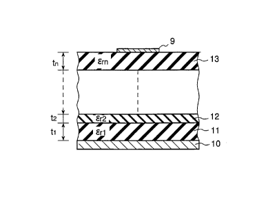
FIG. 1 is a sectional view showing the structure of an
antenna apparatus according to the embodiment 1 of the
present invention. In the drawing, numeral 9 designates a
radiating element or a major radiating conductor which is
fed. Both of feed and no-feed radiating conductors are
considered to be applied to a major radiating material of
the antenna apparatus. In the embodiment 1, a radiating
element 9 as a major radiating conductor is described for a
feed radiating conductor having feeding means such as
feeding circuit as one example for convenience' sake of
description. Numeral 10 designates a conductive plate or
ground plate; numeral 11 designates a first dielectric
layer; numeral 12 designates a second dielectric layer;
numeral 13 designates a n-th dielectric layer. The
CA 02204326 1997-0~-02
dielectric layers are n layers in total, and stacked
between the radiating element 9 and the conductive plate
10. The dielectric layers have t" tZ~ ..., tn in
thickness, and ~rl~ ~r2' ' ~rn in dielectric constant.
Note that the dielectric layers are secured by a method
such as screwing or packing after stacked.
Next, the operation will be described.
The radiating element 9 is driven by electric waves
fed through the feeding means such as feeding circuit. The
driven radiating element 9 radiates radio waves in the air.
In this case, in the antenna apparatus formed by the
minimum thickness as described below, the radiation is
conducted, which ensures a desired radiation level to a
direction of low elevation angle, and desired reflective
characteristic and operation band.
The thicknesses tl, tZ~ ..., tn of the dielectric
layers in the antenna apparatus are defined by the
following manner. The dielectric constant l~rett of the
antenna is first described. Typically, a dielectric
constant of an antenna means that of the very dielectric
layer where a dielectric layer having one layer only is
considered to be formed between the radiating element 9 and
conductive ground plate 10. In a case that a plurality of
dielectric layers are formed as shown in FIG. 1, when the
plurality of dielectric layers are replaced by a single
dielectric layer so as not to change an interval between
the radiating element 9 and conductive ground plate 10, the
size of the radiating element 9, and the operation
frequency of the radiating element 9, the dielectric
CA 02204326 1997-0~-02
constant ~reff of the single dielectric layer is
approximated by the following equation (1):
~ref f = (tl + t7 + ~ tn)/ (tl/~rl + t~ + ... + t~/~r~)
. . . (1)
On the other hand, a radiating pattern of the
radiating element 9 is defined by the dielectric constant
reff of the antenna and the configuration of the radiating
element 9. Accordingly, when the configuration of the
radiating element 9 is defined in advance, the dielectric
constant ~reff of the antenna is defined, which is required
to obtain a desired beam width (beam spread) capable of
ensuring a desired radiation level to a direction of low
elevation angle.
Next, the operation band and reflection loss of the
radiating element 9 is considered. The operation band of
the radiating element 9 in which VSWR, index of reflection
loss, is not more than "s" is expressed by the following
equation (2):
BW = (s-1)/(QT*~s) ...(2)
Note that QT is quality factor of the radiating
element 9. The QT is determined mainly by the dielectric
constant ~relf ~f the antenna, the configuration of the
radiating element 9, and an interval between the radiating
element 9 and conductive ground plate 10. Consequently,
when the configuration of the radiating element 9 is
determined in advance, the minimum interval t,j~ between the
radiating element 9 and conductive ground plate 10 is
defined by the dielectric constant Er~ of the antenna as
it is required to obtain desired operation band and
CA 02204326 1997-0~-02
reflection characteristics.
As stated above, the dielectric constant ~rei ~ f the
antenna required to obtain a desired beam width, and the
minimum interval t,in between the radiating element 9 and
conductive ground plate 10 required to obtain desired
operation band and reflection characteristics are uniquely
determined. Accordingly, determination of the thicknesses
of the dielectric layers t~-tn to satisfy the following
equations (3) and (4) can obtain the thinnest antenna
capable of ensuring desired characteristics.
2 '-- tn)/ ( tl/~r I + t2 / ~r ~ + ~ ~ ~ + tn / ~r n ) = ~ f f
...(3)
tl + t2 + ~ ~ ~ ~ tn t~in
Note that ~reff iS a dielectric constant of an antenna
defined by a desired beam width; tr~in is the minimum
interval between the radiating element 9 and conductive
ground plate 10 capable of ensuring desired operation band
and reflection characteristics in the dielectric constant
reff -
Assuming that a dielectric having desired dielectric
constant ~ref f and thickness t,in exists, the above
dielectric layer can be achieved by one layer, However,
when a convenient material is not available, a targeted
antenna can be constituted by using a combination of a
plurality of available dielectrics having different
dielectric constants from each other as in the embodiment
1.
As described above, according to the embodiment 1, the
thinnest antenna apparatus capable of ensuring a desired
CA 02204326 1997-0~-02
radiation level to a direction of low elevation angle, and
desired reflection characteristics and operation band may
be provided.
Additionally, as the prior art and the like, in a case
where the major radiating conductor of the antenna
apparatus is not the feed radiating element, but the no-
feed radiating element driven by the feed radiating
element, the aforementioned method is applied to between
the no-feed radiating element and conductive ground plate
10. Similarly, the thinnest antenna apparatus ensuring
desired characteristics can be provided.
In addition, of course, some of a plurality of
dielectric layers can be constituted by air layers as in
the prior art, attained by introducing in calculation the
dielectric constant of the air, and the thickness of the
air layers.
Embodiment 2.
FIG. 2 is a sectional view showing the structure of an
antenna apparatus according to the embodiment 2 of the
present invention. In FIG. 2, numeral 1 designates a feed
radiating element of feed radiating conductor made of
copper, aluminum, and the like formed on a film substrate
17 as described later; numeral 2 designates a no-feed
2~ radiating element or conductor which is a major radiating
conductor. ~'umeral 14 designates a first dielectric plate,
which is rigid; numeral 15 designates a second dielectric
plate, which is rigid, formed of fluorocarbon resin
trademarked by teflon, PPO (polyphenylene oxide), or the
CA 02204326 1997-0~-02
like. Numeral 16 designates a foaming material plate made
of a foaming material such as foaming polyethylene, which
is a dielectric layer also serving as a buffer material;
numeral 17 designates a film substrate formed by etching
the feed radiating element 1 and feeding circuit. These
layers are closely secured by a method, e.g. screwing,
packing, or the like after stacked. Note that parts
similar or corresponding to those denoted in FIGS. 1 and 8A
are denoted by the same reference numerals, and redundant
explanation thereof will be omitted.
In the antenna apparatus, the dielectric is
constituted by the first dielectric plate 14, second
dielectric plate 15, and foaming material plate 16; the
feed radiating element 1 and feeding circuit are
constituted on the film substrate 17. Since the film
substrate 17 is flexible, the film substrate 17 is pressed
against the first dielectric plate 14 to be closely
contacted with the foaming material plate 16 as a buffer
material through the second dielectric plate 15. Thus, it
is constituted such that the plane configuration and
arrangement precision of the film substrate 17 are
maintained. The no-feed radiating element 2 is constituted
by adhering the second dielectric plate 15 to a conductor
foil, e.g. copper foil tape or the like.
Next, the operation is described.
The operation of the antenna apparatus of the
embodiment 2 is similar to that of the prior art: the feed
radiating element 1 is driven by radio waves fed through
the feeding circuit, and the radio waves radiated from the
CA 02204326 l997-0~-02
14
driven feed radiating element 1 are electromagnetically
coupled to the no-feed radiating element 2, thus driving
the no-feed radiating element 2. The driven no-feed
radiating element 2 radiates spatially the radio waves.
The thicknesses of the first dielectric plate 14,
second dielectric plate 15, and foaming material plate 16
are defined by a desired beam width, and desired operation
band and reflection characteristics in the same manner as
shown in the above embodiment 1. In this case, though the
film substrate 17 is ignored because of its thin thickness,
the dielectric constant of the film substrate 17 can be
introduced in calculation. The thinnest antenna apparatus
that ensures a desired radiating level to a direction of
low elevation angle, a desired operation band, and low
reflection losses can be provided by setting the thickness
of such a dielectric layer.
Typically, in the antenna apparatus of the prior art,
the embodiment 1, or the like, many of the radiating
elements and feeding circuits are constructed by etching a
dielectric substrate with a conductive film which is
expensive, thus resulting in higher manufacturing cost. On
the other hand, the antenna apparatus of the embodiment 2
can control to lower manufacturing cost because of using
the film substrate 17.
Further since the film substrate 17 is flexible, it is
hard to keep the arrangement precision. However, in the
antenna apparatus of the embodiment 2, the film substrate
17 is arranged on the first dielectric plate 14 which is
rigid; the foaming material plate 16 as a buffer material
CA 02204326 1997-0~-02
is arranged on the first dielectric plate 17; the second
dielectric plate 15 which is rigid is arranged thereon to
press the film substrate 17; accordingly plane
configuration and arrangement precision of the feed
radiating element 1 in the film substrate 17 can be kept at
high precision, thereby ensuring the quality of the antenna
apparatus to conduct a desired mode drive at high
precision. In addition, lightening of the antenna
apparatus is attained by use of the foaming material plate
16 with light weight as a dielectric layer.
Embodiment 3.
FIG. 3 is a sectional view showing the structure of an
antenna apparatus according to the embodiment 3 of the
present invention. In the drawing, numeral 1 designates a
feed radiating element; numeral 2 designates a no-feed
radiating element; numeral 18 designates a feeding circuit,
formed on a first dielectric layer 11, for feeding the feed
radiating element 1. Note that parts similar or
corresponding to those denoted in FIG. 1 or 2 are denoted
by the same reference numerals, and redundant explanation
thereof will be omitted.
As stated in the above embodiment 1, the thicknesses
t,-t~ of the dielectric layers are defined by only
characteristics which are required for the radiating
element. The second to n-th dielectric layers are not
required to form the feeding circuit 18; in addition
thicknesses of the dielectric layers are concerned only at
the perimeters of the feed radiating element 1 and no-feed
CA 02204326 l997-0~-02
16
radiating element 2, while the dielectric layers are not
required electrically at the other parts. For this reason,
in the embodiment 3, the perimeters of the feed radiating
element 1 and no-feed radiating element 2 are left, while
the second to n-th dielectric layers are removed.
As described above, according to the embodiment 3, the
perimeters of the feed radiating element 1 and no-feed
radiating element 2 are left, while the second to n-th
dielectric layers are removed; accordingly, lightening can
be attained as compared with the above embodiment 1.
Though the no-feed radiating element 2 of which the
major radiating conductor is not fed is shown in the above,
it is possible to adopt a constitution such that all or
part of the dielectric layers are removed by eliminating
the perimeter of the major radiating conductor also in case
of a radiating conductor in which the major radiating
conductor is fed like the above embodiment 1, thus
attaining lightening similarly.
Embodiment 4.
FIG. 4 is a sectional view showing the structure of an
antenna apparatus according to the embodiment 4 of the
present invention. Note that parts similar or
corresponding to those denoted in FIG. 2 are denoted by the
same reference numerals, and redundant explanation thereof
will be omitted. The embodiment 4 forms thinly in such a
manner that the thickness of the second dielectric plate 15
in the above structure of the embodiment 2 is eliminated at
its perimeter.
CA 02204326 1997-0~-02
As stated in the above embodiment 3, the dielectric
layers are concerned only at the perimeters of the feed
radiating element 1 and no-feed radiating element 2, while
the dielectric layers such as the second dielectric plate
15 and foaming material plate 16
are not required electrically at the other parts. In the
embodiment 4 the second dielectric plate 15 and foaming
material plate 16 play a role to press the film substrate
17 from the top to contact closely it with the first
dielectric plate 14, thus being not eliminated completely,
just keeping the second dielectric plate 15 thinly.
As described above, according to the embodiment 4, the
thickness of the second dielectric plate 15 is formed
thinly such that the perimeter of the no-feed radiating
element 2 is eliminated. Accordingly, the same effects as
those of the above embodiment 2 are obtained; also an
antenna apparatus with lighter weight as compared with the
above embodiment 2 can be achieved.
Embodiment 5.
FIG. 5 is a sectional view showing the structure of an
antenna apparatus according to the embodiment 5. In the
drawing, numeral 19 designates a third dielectric layer;
numeral 20 designates a spacer (thickness holding
structure) provided between the first dielectric layer 11
and the third dielectric layer 19. ~ote that parts similar
or corresponding to those denoted in FIG. 1 are denoted by
the same reference numerals, and redundant explanation
thereof will be omitted. Here, the first dielectric layer
CA 02204326 l997-0~-02
18
11 and third dielectric layer 19 is constituted by a
material with high rigidity. The second dielectric layer
12 is constituted by a material with low rigidity such as
foaming material plate. The spacer 20 is made of at least
a material with at least a higher rigidity than those of
the first and second dielectric layers 11, 12. Disposition
of the spacer 20 can employ a method such that the spacer
20 is inserted into a hole or opening formed in the second
dielectric layer 12 upon stacking the second dielectric
layer 12.
As the second dielectric layer 12 shown in FIG. 5, for
the purposes of reducing dielectric losses and pressing
flexible members such as film substrate and the like, there
is a case that a material with low rigidity as a foaming
material plate or the like is used. In this case, the
dielectric layer with low rigidity, however, causes
deformation not to maintain the thickness precision,
thereby failing to ensure desired characteristics. For
this reason, in the embodiment 5, the spacer 20 is disposed
between the first dielectric layer 11 and third dielectric
layer 19. In this manner, the thickness precision of the
second dielectric layer 12 with low rigidity is maintained.
Additionally, in case of application of a spacer 20
made of a metal, when disposition place of the spacer 20 is
near the radiating element 9 to an extent such that a shape
of electric field distribution and a resonance frequency of
the radiating element 9 change, a material of the spacer 20
had better employ a dielectric instead of metals.
As stated above, according to the embodiment 5, the
CA 02204326 1997-0~-02
19
thickness precision of the second dielectric layer 12 which
is constituted by a material with low rigidity such as
foaming material plate can be maintained. With this
manner, when the dielectric layer with low rigidity such as
foaming material plate is employed, the quality of the
antenna apparatus can be maintained.
Embodiment 6.
FIG. 6 is a sectional view showing a structure of an
antenna apparatus according to the embodiment 6. In the
drawing, numeral 21 designates a caulking nut; numeral 22
designates a screw meshing with the caulking nut 21; these
caulking nut and screw form a thickness holding structure.
Note that parts similar or corresponding to those denoted
in FIG. 2 are denoted by the same reference numerals, and
redundant explanation thereof will be omitted.
In the structure of the above embodiment 2, the
embodiment 6 is constituted by disposing the caulking nut
21 in the conductor ground plate 10, contacting the head of
the caulking nut 21 with the second dielectric plate 15,
and securing the second dielectric plate 15 and caulking
nut 21 with a screw 22 through hole or groove provided in
the second dielectric plate 15. Additionally, when a metal
is employed for the caulked nut 21 and screw 22, when
disposition place of the spacer 20 is near the feed
radiating element 1 and no-feed radiating element 2 to an
extent such that a shape of electric field distribution of
and a resonance frequency due to the feed radiating element
1 and no-feed radiating element 2 change, a material of the
CA 02204326 1997-0~-02
caulking nut 21 and screw 22 had better employ a dielectric
instead of metals.
As described above, according to the embodiment 6, the
precision of the interval precision between the conductive
ground plate 10 and second dielectric plate 15 can be
maintained through the caulked nut 21, and also according
to the thickness precision of the first dielectric plate
14, the disposition precision of the film substrate 17 in
which the feed radiating element 1 and feeding circuit are
formed, and the thickness precision of the foaming material
plate 16 as a dielectric layer can be maintained, thus
keeping the quality of the antenna apparatus.
Embodiment 7.
FIGS. 7A-7C are schematic diagrams showing the
structure of an antenna apparatus according to the
embodiment 7; FIG. 7A is a longitudinal sectional view;
FIG. 7B is a sectional view along the line I-I of FIG. 7A.
In the drawing, numeral 23 designates a rotary joint;
numeral 24 designates a feeding circuit disposed on a film
substrate 17; numeral 25 designates a connection of the
rotary joint and the feeding circuit 24. The rotary joint
23 is a joint in which the top part in the drawing becomes
rotatable to the bottom part in the drawing while keeping
the connection. In the embodiment 7, it is constituted
such that the top part in the drawing of the rotary joint
23 is secured to the other parts of the antenna apparatus,
thus rotating together. Note that parts similar or
corresponding to those denoted in FIG. 2 are denoted by the
CA 02204326 1997-0~-02
21
same reference numerals, and redundant explanation thereof
will be omitted.
In the embodiment 7, the antenna apparatus of the
above embodiment 2 is constituted by an array-antenna, and
also fed through the rotary joint 23. A rotating means
such as motor for rotating the top part in the drawing is
appropriately installed at the rotary joint 23. As shown
in FIG. 7B, it is constituted such that the feed radiating
element 1 is not disposed on the connection 25 between the
rotary joint 23 and feeding circuit 24 so as to conduct
effective feeding to the other feed radiating element 1.
In this case, a constitution such that the feed radiating
element 1 disposed on the center of a feed radiating
elements 1 group facilitates a desired radiating pattern
relatively. However, selecting an element array such that
the feed radiating element 1 is disposed above the
connection 25, the feeding circuit 24 and feed radiating
element 1 have to be constituted with different layers. The
number of the parts increases to boost up the manufacturing
cost of the antenna apparatus, thus not adopting such an
element array.
As described above, according to the embodiment 7,
since the antenna apparatus is rotatable mechanically as a
structure with the rotary joint 23, the radiation direction
can be rotated freely, thereby forming an antenna apparatus
capable of utilizing for automobile mounting of vehicle
satellite communication and the like. In addition, it is
constituted such that the feed radiating element 1 is not
disposed on the connection 25 upon connecting with the
CA 02204326 1997-0~-02
rotary joint 23; accordingly, there are no needs that the
feeding circuit 24 is arranged with the feed radiating
element 1 separately, and that the connection with the
feeding circuit 24 is used with a special rotary joint off
the rotation center; the manufacturing can be performed at
low cost; a rotatable array antenna capable of feeding each
feed radiating element 1 effectively may be constituted.
In the above, shown is one example that the rotary
joint 23 is applied to an antenna apparatus having the feed
radiating element 1 and no-feed radiating element 2, which
is a major conductor. The rotary joint 23 also be applied
to an antenna apparatus in which a major radiating
conductor is a feed radiating conductor, A constitution as
shown in FIG. 7C corresponds to this example. The cross
section along the line II-II of FIG. 7C is identical to
that of FIG. 7B. In the drawing, note that parts similar
or corresponding to those in FIGS. 7A and 7B are denoted by
the same reference numerals, and redundant explanation
thereof will be omitted. Corresponding to said
constitution, the rotary joint 23 is connected to the
feeding circuit for feeding the major radiating conductor
as well, thus obtaining the similar effect.
It will be appreciated from the foregoing description
that, according to the first aspect of the present
invention, there is provided the antenna apparatus in which
n dielectric layers having tl-tn in thickness, and ~r!~~r~ in
dielectric constant are respectively stacked between the
major radiating conductor and the ground plate in turn from
CA 02204326 1997-0~-02
23
this ground plate side, the thicknesses t~-tn of the n
dielectric layers are determined so as to satisfy
substantially the following equation with respect to a
dielectric constant ~re~L of the antenna defined by a
desired beam width:
(tl + t~ + ..- + tn)/ (tl/~rL + t~/~r2 + ' + tn/~rn) ~reff
and satisfy substantially the following equation with
respect to the minimum value t~in of the thickness between
the radiating conductor and ground plate capable of
ensuring desired operation band and low reflection losses
in said dielectric constant ~reff:
tl + t~ + ... + tn t,in
Therefore, there is an effect capable of obtaining the
thinnest antenna apparatus which ensures a desired
radiation level to a direction of low elevation angle, and
desired operation band and low reflection losses.
According to the second aspect of this invention, in
the antenna apparatus in which the major radiating
conductor is a feed radiating conductor, it is constituted
such that the thicknesses t,-tn of the n dielectric layers
are defined as described in the above first aspect.
Therefore, there is an effect capable of obtaining the
thinnest antenna apparatus which ensures a desired
radiation level to a direction of low elevation angle, and
desired operation band and low reflection losses.
According to the third aspect of this invention, since
the n dielectric layers include an air layer, there is an
effect such that the total mass can be reduced.
According to the fourth aspect of this invention, in
CA 02204326 1997-0~-02
24
the antenna apparatus in which the major radiating
conductor is a no-feed radiating conductor, it is
constituted such that the feed radiating conductor for
driving the no-feed major radiating conductor and the
feeding circuit for feeding the feed radiating conductor
are arranged on a dielectric layer except the n-th layer.
Therefore, there is an effect capable of obtaining the
thinnest antenna apparatus which ensures a desired
radiation level to a direction of low elevation angle, and
desired operation band and low reflection losses.
According to the fifth aspect of this invention, it is
constituted by arranging a rigid dielectric layer by
forming the feed radiating conductor and feeding circuit
through the film substrate, arranging the buffer material
on the film substrate, and arranging the rigid dielectric
layer on the buffer material. Therefore, there are the
following effects: the manufacturing cost can be controlled
lowly as compared with a case where the feed radiating
conductor and feeding circuit are formed by etching the
dielectric substrate with a conductive film or the like;
also the plane configuration and disposition precision of
the feed radiating conductor in the flexible film substrate
can be kept at high precision by pressing the rigid
dielectric layer through the buffer material; the quality
of the antenna apparatus can be ensured so as to drive a
desired mode at high precision.
According to the sixth aspect of this invention, since
the rigid dielectric layer is made of fluorocarbon resin or
polyphenylene oxide, which is easily processed with high
CA 02204326 1997-0~-02
rigidity. Therefore, the plane configuration and
disposition precision of the feed radiating conductor in
the flexible film substrate can be kept at high precision
by pressing the rigid dielectric layer through the buffer
material, thereby having the above effect.
According to the seventh aspect of this invention,
since the buffer material is made of foaming resin, there
is an effect that commercial foaming resin can be easily
prepared, resulting in lightening the whole apparatus.
According to the eighth aspect of this invention, in
the above fifth aspect, it is constituted such that a
portion in contact with the buffer material of the rigid
dielectric layer is left, and that dielectric layers on the
side of the major radiating conductor from said portion are
removed except the perimeters of the major radiating
conductor and feed radiating conductor. Accordingly, there
are effects such that the plane configuration and
disposition precision of the feed radiating conductor are
secured against pressure to the rigid dielectric layer
ZO through the buffer material, thereby ensuring the quality
of the antenna apparatus, and that lightening of the
antenna apparatus can be attained by elimination of the
dielectrics except the portion requiring dielectric
thickness.
According to the ninth aspect of this invention, in
the above fourth aspect, since all or part of the
dielectric layers on the side of the above major radiating
conductor are removed from the feed radiating conductor and
feeding circuit except the perimeters of the major
CA 02204326 1997-0~-02
26
radiating conductor and feed radiating conductor, there is
an effect such that an antenna having lighter weight can be
achieved by elimination of the dielectrics except the
portion requiring the dielectric thickness.
According to the tenth aspect of this invention, in
the above second aspect, since it is constituted such that
all or part of the dielectric layers are removed except the
perimeters of the major radiating conductor, there is an
effect such that an antenna having lighter weight can be
achieved by elimination of the dielectrics except the
portion requiring the dielectric thickness.
According to the eleventh aspect of this invention, it
is constituted such that a thickness holding structure for
keeping almost in constant the thickness of the dielectric
layer with low rigidity is arranged on any one of the
dielectric layers except the n-th layer. Therefore, for
the purposes of reducing dielectric losses and pressing
flexible members such as film substrate and the like, even
in a case that a material with low rigidity as a foaming
material plate or the like is used, there is an effect such
that the thickness precision of the dielectric layer with
low rigidity is maintained, thereby keeping the quality of
the antenna apparatus.
According to the twelfth aspect of this invention,
since the thickness holding structure is formed by use of
the spacer that is intervened between the first dielectric
layer and the third dielectric layer which are higher in
rigidity than the second dielectric layer with low
rigidity, and that is contained in the second dielectric
CA 02204326 1997-0~-02
layer, there is an effect such that the thickness precision
of the dielectric layer with low rigidity is maintained,
thereby keeping the quality of the antenna apparatus as
described above.
According to the thirteenth aspect of this invention,
since the spacer is made of a material having a rigidity
higher than that of the second dielectric layer, there is
an effect such that the thickness precision of the
dielectric layer with low rigidity is maintained, thereby
keeping the quality of the antenna apparatus as described
above.
According to the fourteenth aspect of this invention,
since the spacer is constituted in such a manner that the
caulking nut is intervened between the first and second
dielectric layers, and that the ground plate meshes with
the screw via the opening through the third dielectric
layer from its top, there is an effect such that
cooperation between the caulking nut and screw can enhance
further the capability of keeping the thickness precision
by means of the spacer.
According to the fifteenth aspect of this invention,
since it is constituted such that the rotary joint is
connected with the feeding circuit so as to feed the major
radiating conductor, and that said major radiating
conductor is arranged to prevent the feeding circuit and
the connection with the rotary joint from overlapping, the
antenna apparatus can be pivoted mechanically to pivot
freely its radiation direction. Therefore, there is an
effect such that an antenna apparatus applicable to
CA 02204326 1997-0~-02
28
automobile mounting of vehicle satellite communication and
the like can be achieved.
According to the sixteenth aspect of this invention,
since the rotary joint is connected to the feeding circuit
for feeding the feed radiating conductor, and that the feed
radiating conductor is arranged to prevent the feeding
circuit and the rotary joint from overlappin~ at the
connection, the antenna.apparatus can be pivoted
mechanically to pivot freely its radiation direction as
described above. Therefore, there is an effect such that
an antenna apparatus applicable to automobile mounting of
vehicle satellite communication and the like can be
achieved.