Note: Descriptions are shown in the official language in which they were submitted.
CA 02204409 1994-0~-02
AMPLIFIER CIRCUIT AND METHOD OF TUNING THE
AMPLIFIER CIRCUIT
Field of the Invention
The present invention relates generally to amplifier circuits, and
more particularly to Doherty type amplifier circuits.
Background of the Invention
Conventional Doherty type amplifier circuits are well known to
those skilled in the art. "A New High Efficiency Power Amplifier for
Modulated Waves~, Proceedings of the Institute of Radio Engineers, Vol.
24, No. 9, pp. 1 163-1 182. (September 1936). However, it is also well
15 known that conventional Doherty type amplifiers typically have relatively
poor linearity. In addition, their linearity is typically inversely proportionalto their efficiency. Thus, conventional Doherty type amplifiers that
provide good efficiency have poor linearity. Due to their poor linearity,
conventional Doherty type amplifier circuits are not well suited to many
20 applications, such as multicarrier power amplifier applications in cellular
base station equipment. Accordingly, there exists a need for a Doherty
type amplifier circuit with improved linearity.
Summary of the Invention
In order to address this need, the present invention provides an
improved amplifier circuit and a method of tuning a Doherty type amplifier
circuit. According to one aspect of the present invention, the amplifier
circuit comprises a first amplifier having a carrier amplifier and a peak
30 amplifier configured in a Doherty arrangement, a second amplifier having
a carrier amplifier and a peak amplifier configured in a Doherty
arrangement, and a combination circuit responsive to the first and
second amplifier. The first amplifier produces a substantially linear first
output signal over a first frequency bandwidth. The second amplifier
35 produces a substantially linear second output signal over a second
CA 02204409 1994-0~-02
bandwidth. The combination circuit is responsive to the first and second
output signal and produces a third output signal that is substantially
linear over a third frequency bandwidth. The third frequency bandwidth
is greater then either the first or second frequency bandwidths.
According to another aspect of the present invention, the amplifier
circuit comprises a carrier amplifier producing a carrier amplifier output
signal, a peaking amplifier coupled to the carrier amplifier in a Doherty
configuration, and a combination circuit responsive to the carrier
10 amplifier and the peaking amplifier. The peaking amplifier is voltage
biased to produce an adjusted intermodulation product signal. The
combination circuit combines the adjusted modulation product signal
with the carrier amplifier output signal to produce a substantially
linearized amplifier circuit output signal.
1 5
The method of tuning a Doherty type amplifier circuit includes the
steps of providing a Doherty type amplifier, measuring intermodulation
performance of the Doherty type amplifier as a function of peaking
amplifier bias voltage, and selecting a peaking amplifier bias voltage
20 based on the measured intermodulation performance. The invention
itself, together with its attendant advantages, will best be understood by
reference to the following detailed description, taken in conjunction with
the accompanying drawings.
Brief Description of the Drawings
FIG. 1 is a circuit schematic of a Doherty type amplifier circuit.
FIG. 2 is a graph of intermodulation products for the Doherty type
amplifier of FIG. 1.
FIG. 3 is a circuit diagram of a feedforward amplifier using the
Doherty type amplifier of FIG. 1.
FIG. 4 is a block diagram illustrating a parallel Doherty type
amplifier arrangement.
FIG. 5 is a flow chart of a method of tuning a Doherty tpe amplifier.
FIG. 6 is a particular embodiment of a matching circuit.
CA 02204409 1994-0~-02
Detailed Description
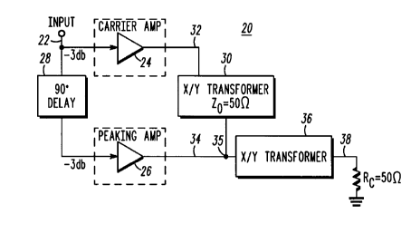
Referring to FIG.1, an amplifier circuit 20 including a carrier
amplifier 24 and a peaking amplifier 26 configured in a Doherty
arrangement is illustrated. The amplifiers 24 and 26 each receive a bias
voltage. The amplifier circuit 20 has an input 22 and an output 38. The
amplifier circuit includes a delay line 28, preferably providing a 90
degree delay, and a transformer line 30. The carrier amplifier 24
produces an output signal that is transmitted over a phasing line 32 and
over the transformer line 30. The peaking amplifier 26 provides an
output signal that is transmitted over a second phasing line 34. The
output signals from the carrier and peaking amplifiers 24 and 26 are
joined in a combination circuit 35 such as a common node, transmitted
over a transformer line 36, and finally outputted at the amplifier circuit
1 5 output 38.
The carrier amplifier 24 preferably a metal oxide semiconductor
field effect transistor (MOSFET) type amplifier, such as a MRF183 Series
amplifier available from Motorola operating in a class AB mode. The
peaking amplifier 26 is preferably a MOSFET type amplifier such as a
MRF183 Series amplifier available from Motorola operating in a class C
mode. The MRF 183 Series amplifiers are available from Motorola at
5008 E. McDowell Road, Phoneix, Arizona, 85008. The delay line 28 is
preferably implemented with microstrip or stripline technology in a
manner known to those of ordinary skill. The transformer line 30 has an
impedance of about fifty ohms and is a quarter wavelength. In the
preferred embodiment, the transformer line 36 is also quarter wavelength
and has an impedance of about thirty five ohms. The peaking amplifier
26 is responsive to the delay line 28 and is coupled to the phasing line
34. The transformer line 30 is responsive to the carrier amplifier 24 and
interconnects the outputs from the carrier and peaking amplifiers 24 and
26. During operation, the carrier amplifier 24 is voltage biased for linear
operation while the peaking amplifier 26 is voltage biased for nonlinear
operation. Over a predetermined frequency range, the peaking amplifier
- CA 02204409 1994-0~-02
26 produces intermodulation products such as third order
intermodulation products, that destructively combine with intermodulation
products from the carrier amplifier 24 such that the entire amplifier circuit
20 operates substantially linearly. However, due to fluctuations in
individual amplifiers, the amplifier circuit 20 should be tuned to improve
linearity of performance over the desired frequency range.
A preferred method of tuning the amplifier circuit 20 to be
substantially linear over a certain frequency range will now be described.
First, determine baseline intermodulation (IM) product performance by
subjecting the amplifier circuit 20 with a two tone excitation signal.
Second, based on the measured IM performance, voltage bias the carrier
amplifier 24 based on application specific design considerations such as
gain, IM performance, and efficiency. Third, sweep IM performance of the
amplifier circuit 20 as a function of the peaking amplifier 26 bias voltage.
An illustration of an exemplary peaking amplifier sweep is shown in FIG.
2. If good IM cancellation is observed, adjust the bias voltage of the
peaking amplifier 26 to finely tune amplifier circuit 20 to further reduce IM
products.
However, If no IM cancellation is observed, then rematch the
carrier amplifier 24 and/or the peaking amplifier 26, and/or adjust the
length of phasing lines 32 and 34. After adjusting components within
amplifier circuit 20, repeat steps one to three above until satisfactory IM
performance is achieved. A flow chart of the preferred method is
illustrated in FIG. 5, and an example of a Doherty amplifier that has been
tuned is disclosed in FIG. 6.
Referring to FIG. 3, another preferred embodiment of an amplifier
circuit 150 is illustrated. The amplifier circuit 150 includes first 154, a
second 156, and a third 158 Doherty type amplifiers that are preferably in
a parallel arrangement. Each of the amplifiers 154,156, and 158 is
responsive to a driver amplifier 152 that receives an input signal 164 and
produces a driver signal 160. The driver signal 160 is fed into the input
of each of the amplifiers 154,156, and 158. Each of the amplifiers 154,
CA 02204409 1994-0~-02
156, and 158 produces an amplified output that is joined at a common
node 162 and sent to an output 166 of the amplifier circuit 150. Each of
the Doherty type amplifiers 154,156, and 158 is preferably substantially
similar in construction to the amplifier 20 illustrated in FIG.1 and tuned to
5 operate substantially linearly as described by the preferred tuning
method set forth above.
However, each of the amplifiers 154,156, and 158 are designed
to operate in a substantially linear mode over a different frequency band.
10 For example, the first amplifier 154 may be designed to operate
substantially linearly between about 865 MHz and about 875 MHz, the
second amplifier 156 may be designed to operate substantially linearly
between about 875 and about 885 MHz, and the third amplifier 158 may
be designed to operate substantially linearly from about 885 MHz to
15 about 895 MHz. In the preferred embodiment of FIG. 4, the first amplifier
154 has a center frequency of about 870 MHz, the second amplifier 156
has a center frequency of about 880 MHz, and the third amplifier 158 has
a center frequency of about 890 MHz. A Doherty type amplifier may be
tuned to operate substantially linearly over a narrow frequency range.
20 The specific frequency bandwidth of linear operation may be determined
by adjusting a matching circuit within the Doherty amplifier, by adjusting
the lengths of phasing lines, such as phasing lines 32 and 34 in amplifier
20, or by adjusting bias voltages of the carrier or peaking amplifiers 24
and 26. Alternatively, each of the amplifiers 154,156, and 158, may be
25 operating at a different transition voltage leading to varying frequency
bands of linearity.
The Doherty amplifier architecture has an intrinsic bandwidth
limitation. The limitation is due to circuit loading of the carrier amplifier by30 the peaking amplifier. The degree of circuit loading is determined by the
peaking amplifier output matching circuit reactance, as well as the
intrinsic reactance of the device, and the associated parasitic reactance
of the device package. Feedforward amplifiers generally require
broadband main amplifiers to minimize time delays through active
35 devices and to facilitate broadband carrier cancellation.
CA 02204409 1994-0~-02
In the preferred embodiment where several Doherty amplifiers are
parallel combined, the intrinsic bandwidth limitation can be overcome by
using a tuning methodology which extends Doherty amplifier bandwidth
and substantially maintains intermodulation performance, gain flatness,
and high efficiency. The tuning methodology to achieve a total system
bandwidth of X MHz consists of several parts.
Each carrier amplifier and peaking amplifier stage (for N total
Doherty stages in parallel) are matched for a desired intermodulation,
efficiency, and gain flatness over a bandwidth of X/N MHz. Matching
circuits are composed of conventional discrete reactive elements such as
capacitors, inductors and/or distributed transmission lines, in both series
and parallel configurations for RF circuits. An example of a tuned
matching circuit is shown in FIG. 6. By matching carrier and peaking
amplifier stages for desirable performance over a narrower X/N MHz
bandwidth, intermodulation performance and efficiency for the total
Doherty configuration is enhanced. For example, if there are three
Doherty stages in parallel, and the total system bandwidth requirement is
30 MHz, then each of the peaking and carrier amplifiers should be
matched for a 10 MHz fractional bandwidth (X = 30 MHz, N = 3). If the
band center of the amplifier were 855 MHz, then one Doherty stage
would be matched over the 840-850 MHz band, the second Doherty
stage would be matched for the 850-860 band, and the final Doherty
stage would be matched for the 860-870 MHz band. When the stages
are paralleled, the gain responses overlap, resulting in a flat gain
response over the full X MHz bandwidth. A similar bandwidth extension
mechanism is used in developing wideband filter designs.
Each carrier amplifier and peaking amplifier in a Doherty circuit is
preferably coupled to provide proper power combining between the
amplifiers. This coupling is often achieved using a transmission line of
approximately ~/4 wavelengths. Since the transmission line (or phasing
line) is frequency sensitive, desirable coupling of the carrier and peaking
amplifier for maximum power combining occurs at a single frequency.
CA 02204409 1994-0~-02
Therefore, Doherty efficiency (dependent on peaking amplifier circuit
loading) and intermodulation performance (dependent on carrier
amplifier output loading) are enhanced when phasing line optimization is
performed over a X/N MHz bandwidth, rather than the entire X MHz
5 bandwidth. The tuning methodology thus provides that the phasing line
length of each N Doherty amplifier uses a phasing line matched for a
different X/N MHz fractional bandwidth. Using the above example, three
different phasing line lengths would be used. Referring to the above
example again, the 840-850 MHz Doherty stage would have ~/4 phasing
line length of ~845 MHz/4. The 850-860 MHz Doherty stage would have a
~/4 phasing line length of ~855 MHz/4. The 860-870 MHz Doherty stage
would have a ~/4 phasing line length of ~865 MHz/4.
Each Doherty amplifier achieves improved gain flatness and
15 intermodulation performance with an adjustment to the peaking amplifier
bias. Therefore, each Doherty amplifier of bandwidth X/N MHz has its
bias set for a desired gain flatness and intermodulation performance.
However, some parasitic loading effects due to module paralleling may
occur, perturbing the parallel configuration intermodulation and/or gain
20 flatness. The preferred embodiment for the paralleled Doherty
configuration includes a final adjustment of each Doherty amplifier's
peaking amplifier bias voltage to simultaneously adjust the Doherty main
amplifier intermodulation performance, efficiency, and gain flatness.
Since the bias adjustment involves the simultaneous optimization of
2'5 three parameters (gain, flatness, IM, efficiency), a bias adjustment
algorithm is typically used. The bias adjustment algorithm is best
described in terms of a flow chart.
Improved feedforward main amplifier Doherty amplifier
30 performance is realized when IM performance, bandwidth, gain,
efficiency, and group delay targets are all met substantially
simultaneously.
By providing a plurality of Doherty type amplifiers that each
35 operate substantially linearly over a different frequency band, the
. CA 02204409 1994-0~-02
amplifier circuit 150 may operate substantially linearly over a greater
frequency band then any of the individual Doherty amplifiers. In the
particular example of FIG. 3, the amplifier circuit 150 operates
substantially linearly over the frequency band of about 865 MHz to about
895 MHz. Accordingly, the amplifier circuit 150 has the benefit of
operating efficiently by using Doherty type amplifiers and
advantageously operates substantially linearly over a relatively wide
bandwidth.
The above described preferred embodiment provides many
benefits. For example, the group delay through a Doherty amplifier will
be higher than in a conventional amplifier due to the inherent
bandlimited nature of the Doherty circuit. The preferred embodiment
reduces the group delay through the Doherty amplifier. Also, in
multicarrier amplifier applications, it is important to "randomize" the
phase relationships as much as possible between the multiple
intermodulation products which add vectorially at a given frequency. A
phase offset (randomization) is introduced between intermodulation
products generated in each of the parallel Doherty stages. The phase
offset occurs because each Doherty stage has a unique matching
structure, a unique phasing line length, and a unique peaking amplifier
bias set point. The result is the multicarrier intermodulation products add
vectorially to a peak value less often than in a conventional parallel
amplifier design, producing a lower average intermodulation level. In
addition, the preferred X/N MHz design method increases the bandwidth
of an inherently bandlimited Doherty amplifier, which substantially
reduced impact on gain, efficiency and intermodulation performance.
FIG. 4 illustrates a preferred embodiment of a feedforward
amplifier circuit 100. The amplifier circuit 100 includes a main amplifier
106 and an error amplifier 114. The amplifier circuit 100 includes an
input 102, a first coupler 104, a second coupler 108, a third coupler 1 12,
and a fourth coupler 116. The amplifier circuit 100 further includes a first
delay line 110 and a second delay line 1 16. The first coupler 104
samples an RF input signal received at the input 102 and produces a
. CA 02204409 1994-0~-02
clean signal that is delayed by delay line 110. The second coupler 108
samples the output 120 of the main amplifier 106. The third coupler 112
receives the sampled output signal from coupler 108 and combines the
output signal from the output 120 of main amplifier 106 with the delayed
5 version of the input signal sampled by the first coupler 104. The output of
the third coupler is preferably an error signal that is amplified by error
amplifier 114 to produce an amplified error signal 118. The amplified
error signal 118 is combined by the fourth coupler 116 with a delayed
output signal 122 that is produced by the second delay line 116. By
10 combining the delayed output signal 122 with the amplified error signal
116, the resulting output 118 has a reduced level of error relative to the
output signal 120. In this manner, at least a portion of the error due to
nonlinearity due to the main amplifier 106 is cancelled by the fourth
coupler 116 to produce a more linear output 118. In the preferred
15 embodiment, the main amplifier 106 is a Doherty type amplifier, such as
the amplifier circuit 20 illustrated in FIG. 1, that has been tuned according
to the above-described tuning method.
The Doherty configured main amplifier 106 provides a significant
20 increase in direct current (DC) to RF conversion efficiency in the
feedforward amplifier circuit 100. The efficiency improvement over
conventional feed forward amplifier circuits may be about 40%, far
exceeding other conventional efficiency enhancement techniques such
as harmonic termination. For small fractional bandwidths (typically less
25 than 1 %), the Doherty configured main amplifier 106 may also improve
intermodulation performance. Further, Doherty configured main
amplifiers may be employed with large fractional bandwidths.
Further advantages and modifications of the above described
30 apparatus and method will readily occur to those skilled in the art. The
invention, in its broader aspects, is therefore not limited to the specific
details, representative apparatus, and illustrative examples shown and
described above. Various modifications and variations can be made to
the above specification without departing from the scope or spirit of the
35 present invention, and it is intended that the present invention cover all
CA 02204409 1994-0~-02
-10-
such modifications and variations provided they come within the scope of
the following claims and their equivalents.