Note: Descriptions are shown in the official language in which they were submitted.
CA 02204416 1997-OS-02
WO 96/15612 PGT/US95/14829
The present invention relates to communications systems and in
particular to computer assisted digital communications including data, fax,
digitized voice and caller identification information.
A wide variety of communications alternatives are currently
available to telecommunications users. For example, facsimile transmission of
printed matter is available through what is commonly refen~ed to as a stand-
alone fax machine. Alternatively, fax-modem communication systems are
currently available for personal computer users which combine the operation
of a facsimile machine with the word processor of a computer to transmit
documents held on computer disk. Modem communication over telephone
lines in combination with a personal computer is also known in the art where
file transfers can be accomplished from one computer to another. Also,
simultaneous voice and modem data transmitted over the same telephone line
has been accomplished in several ways.
The increased accessibility provided by telephone services and
modems raises problems for controlling access to computer systems.
Computer security systems have been developed which incorporate password
programs to control access. These programs often monitor the number of
times a particular user has logged onto a system. Systems which restrict
access by limiting the number of attempted accesses in a given time period or
by limiting the number of attempted accesses for a given password enable
iutauthorized users to "tie up" the system while they attempt to gain
unauxhotized access. When the system is tied up, authorized users may be
prohibited from accessing the system due to repeated unsuccessful attempts by
unauthorized users. In addition, such systems fail to guarantee that the
unauthorized user will not gain access by guessing a con: ect password
Another personal communications system access problem is
gracefully restricting access to the personal communications system depending
CA 02204416 1997-OS-02
7
on the date or time of day. For example, the system operator of a BBS might
want to restrict modem communications with the BBS between the hours of 8:00
a.m. and 6:00 p.m. to leave time for system maintenance duties.
One attempt at a data communications equipment security device
using caller party directory number was given in European patent 0 X81 528 by
Archibald et al. The Archibald et al. device proposes three courses of action
depending on the calling party directory number (CPDN) of a caller: 1 ) the
data
communications equipment (DCE) can answer the telephone call if the calling
party's CPDN is on the "caller pays" list; 2) the DCE can refuse to answer the
telephone call and then return the telephone call if the CPDN is on the "we
pay"
list; or 3) the DCE can simply not answer, or return, the telephone call if
the
calling party~s CPDN is not found on any of the plurality of lists. However,
the
Archibald et al. device fails to address sophisticated authorization
functions,
such as time of day, and also fails to provide a system for quickly disposing
of
unauthorized callers.
A computer-based multifunction personal communications
system was proposed by Sharma et al. in Canadian Patent 2,104,701, however.
this disclosure does not describe sophisticated caller identification
authorization
means including a means for rapidly disposing of unwanted callers.
Therefore, there is a need in the art for an access control system
for a personal communications system which quickly rejects unauthorized users,
and, preferably denies access before the unauthorized user has an opportunity
to
illegally enter the system. There is a further need for an access control
system
which screens callers without the use of a password system. Finally, there is
a
need in the art for a personal communications access system which screens
calls
based on date and time.
Summary of the Invention
The present invention solves the aforementioned problems and
shortcomings of the existing art and solves other problems not listed above
which will become apparent to those skilled in the art upon reading and
understanding the present specification and claims.
AMENDED SHEET
CA 02204416 1997-OS-02
2a
The present disclosure describes a complex computer assisted
communications system which contains multiple inventions. The subject of the
present multiple inventions is a personal communications system which includes
components of software and hardware operating in conjunction with a personal
computer. The user interface control software operates on a personal computer,
preferably within the Microsoft Windows environment. The software control
system communicates with hardware components linked to the software throu~lh
the personal computer serial communications port. The hardware components
include telephone communication equipment, digital signal processors, and
hardware to enable both fax and data communication with a hardware
components at a remote site connected through a standard telephone line. The
functions of the hardware components are controlled by control software
operating within the hardware component and from the software components
operating within the personal computer.
The major functions of the present system are a telephone
function, a voice mail function, a fax manager function, a multi-media mail
function. a show and tell function, a terminal function and an address book
~ME~dDED SHEET
CA 02204416 1997-OS-02
WO 96/15612 PCT/US95114829
3
function. These functions are described in further detail in U.S. Patent
Application Serial Number 08/002,467 filed January 8, 1993 entitled
"COMPUTER BASED MULTTFUNCTION PERSONAL
CO1~~VILJNICATTONS SYSTEM".
The hardware components of the present system include
circuitry to enable digital data communication and facsimile communication
over standard telephone lines.
The present disclosure also describes a system for personal
communications system access control using a caller ID interface ("CID
interface"). Many standard telephone carriers are encoding caller ID
information which may be n~eived before answering the telephone. One
embodiment of the present invention decodes the incoming caller ID
infon~nation and compares the present caller's identification infon~nation
with a
preprogrammed access matrix to determine if access to the modem is
appropriate. The callers' identification information can be recorded and
statistically tracked regardless of whether the callers are authorized and
regardless of whether each call is answered.
In one embodiment of the present invention, the caller ID
interface incorporates a ring detector, off hook circuit, do holding circuit,
caller )D decoder, relay switching circuit, memory, and processor. The ring
detector circuit is used to enable the caller ID decoder after the first ring,
since most caller ID carriers encode the caller ID information using fi
equency
shift keying transmission after the first telephone ring and before the second
telephone ring. The caller ID decoder is connected to the telephone line
(without answering the call) using the relay switching circuit between the
first
and second telephone ring to receive the incoming caller ID information. The
off hook circuit is used to hang up on an unwanted caller before actually
answering the telephone.
In one embodiment of the present invention the caller ID
interface acquires information about incoming calls by decoding the incoming
caller ID infornation and storing it in memory. Statistical tracking of
callers
is performed on the stored caller ID information if desired by the personal
CA 02204416 1997-OS-02
WO 96/15612 PCT/US95/14829
4
communications system owner. Another embodiment of the present invention
~s by comparing a preprogrammed access mat<-ix to details of the
call such as the caller's name, caller's phone number, the time and date the
call is made, and the number of previous accesses by that caller in a
predefined time flame. A variety of preprogrammed criteria are utilized to
control access to the personal communications system. For example, in one
embodiment, screening by name and telephone number is performed on an
inclusive (or exclusive) basis by preprogrunming the caller ID interface with
the names or telephone numbers of the callers with (or without) access
privileges. The incoming call details obtained from the caller ID information
are then corr>pared to the inclusive (or exclusive) caller list to determine
if the
callers are authorized to access the personal communications system. In an
alternate embodiment of the present invention the caller ID interface hangs up
on an unauthorized caller, preventing the unauthorized caller even brief
access.
Therefore, the present invention solves the deficiencies of the
prior art by providing an apparatus and method for rapid database creation of
incoming calls using caller ID information. One embodiment of the present
invention also quickly rejects unauthorized callers, and may hang up on them
instantly, rather than allow access to the modem The screening process of
the present invention need not use a password for caller authorization, since
the caller ID information can be used to screen out unwanted callers. Yet
another embodiment of the present invention screens incoming calls based on
date and time.
In the drawings, where like numerals describe like components
throughout the several views,
Figure 1 shows the telecommunications environment within
which the present may operate in several of the possible modes of
commuu~ication;
Figure 2 is the main menu icon for the software components
operating on the personal computer;
CA 02204416 1997-OS-02
WO 96/15612 PCT/US95/14829
Figure 3 is a block diagram of the hardware components of the
present system;
Figure 4 is a key for viewing the detailed electrical schematic
diagrams of Figures SA lOC to facilitate understanding of the interconnect
5 between the drawings;
Figures SA SC, 6A-6C, 7A-7C, 8A 8B, 9A 9C and l0A lOC
are detailed electrical schematic diagrams of the circuitry of the hardware
components of the present system;
Figure 11 is a signal flow diagram of the speech compression
algorithm;
Figure 12 is a detailed function flow diagram of the speech
compression algorithm;
Figure 13 is a detailed function flow diagram of the speech
decompression algorithm;
Figure 14 is a detailed function flow diagram of the echo
cancellation algorithm;
Figure 15 is a detailed function flow diagram of the voiceldata
multiplexing function;
Figure 16 is a general block diagram showing one embodiment
of a caller ID interface for a personal communications system;
Figure 17A is a schematic diagram of one embodiment of a
caller m interface for a personal communications system;
Figum 17B is a schematic diagram of an alternate embodiment
of a caller m interface for a personal communications system;
Figure 18 is a block diagram showing the multiple data
message format and single data message format used in standard caller m
encoded transmissions;
Figure 19 is a flowchart showing one embodiment of a caller
ID message format recognition scheme;
Figure 20 is a flowchart of the general operation of one
embodiment of the present invention; and
Figure 21 is a flowchart showing one possible implementation
CA 02204416 1997-OS-02
WO 96115612 PCT/US95114829
6
of a screening mode algorithm
_ ailed Description of the Preferred~ybodiments
In the following detailed description, references made to the
accompanying drawings which form a part hereof and in which is shown by
way of illustration specific embodiment in which the invention may be
p~i~, These embodiments are described in sufficient detail to enable
those skilled in the art to practice and use the invention, and it is to be
understood that other embodiments may be utilized in that electrical, logical,
and structural changes may be made without departing from the spirit and
scope of the present invention. The following detailed description is,
therefore, not to be taken in a limiting sense in scope of the present
invention
as defined by the appended claims
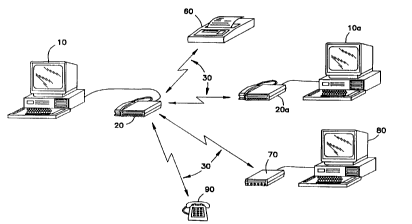
Figure 1 shows a typical arrangement for the use -of the present
system, personal computer 10 is running the software components of the
present system while the hardware components 20 include the data
communication equipment and telephone headset. Hardware components 20
communicate over a standard telephone line 30 to one of a variety of remote
sites. One of the remote sites may be equipped with the present system
including hardware components 20a and software components conning on
personal computer 10a. In one alternative use, the local hardware components
20 may be communicating over standard telephone line 30 to facsimile
machine 60. In another alternative use, the present system may be
communicating over a standard telephone line 30 to another personal
computer 80 through a remote modem 70. In another alternative use, the
present system may be communicating over a standard telephone line 30 to a
standard telephone 90. Those skilled in the art will readily recognize the
wide
variety of communication interconnections possible with the present system by
reading and understanding the following detailed description.
The ornamental featu~ of the hardware components 20 of
Figure 1 are claimed as part of Design Patent Application Number 29/001368,
filed November 12, 1992 entitled "Telephone/Modem case for a Computer-
Based Multifunction Personal Communications System" assigned to the same
WO 96/15612 7 PCT/US95/14829
assignee of the present inventions.
General Overview
The present inventions are embodied in a commercial product by the assignee,
MultiTech Systems, Inc. The software component operating on a personal
computer is sold
under the commercial trademark of MultiExpressPCST"~ personal communications
software
while the hardware component of the present system is sold under the
commercial name of
MultiModemPCST"', Intelligent Personal Communications System Modem. In the
preferred
embodiment, the software component runs under Microsoft~ Windows~ however
those
skilled in the art will readily recognize that the present system is easily
adaptable to run
under any single or mufti-user, single or mufti-window operating system.
The present system is a multifunction communication system which includes
hardware and software components. The system allows the user to connect to
remote
locations equipped with a similar system or with modems, facsimile machines or
standard
telephones over a single analog telephone line. The software component of the
present
system includes a number of modules which are described in more detail below.
Figure 2 is an example of the Windows~-based main menu icon of the
present system operating on a personal computer. The functions listed with the
icons used to
invoke those functions are shown in the preferred embodiment. Those skilled in
the art will
readily recognize that a wide variety of selection techniques may be used to
invoke the
various functions of the present system.
The telephone module allows the system to operate as a conventional or
sophisticated telephone system. The system converts voice into a digital
signal so that it can
be transmitted or stored with other digital data, like computer information.
The telephone
function supports PBX and Centrex features such as call waiting, call
forwarding, caller >D
and three-way
20676038.1
CA 02204416 1999-10-07
CA 02204416 1997-OS-02
WO 96115611 PCT/US95/14829
8
calling. This module also allows the user to mute, hold or record a
conversation. The telephone module enables the handset, headset or hands-
fi~ee speaks telephone operation of the hardware component. It includes on-
scx~n push button dialing speed-dial of stored numbers and digital recording
of two-way conversations.
The voice mail portion of the present system allows this system
to operate as a telephone answering machine by storing voice messages as
digitized voice files along with a time/date voice stamp. The digitized voice
files can be saved and sent to one or more destinations immediately or at a
later time using a queue scheduler. The user can also listen to, forward or
edit the voice messages which have been received with a powerful digital
voice editing component of the present system. This module also creates
queues for outgoing messages to be sent at preselected times and allows the
users to create outgoing messages with the voice editor.
The fax manager portion of the present system is a queue for
incoming and outgoing facsimile pages. In the preferred embodiment of the
present system, this function is tied irno the Windows "print" command once
the present system has been installed This feature allows the user to create
faxes from any Windows~ based document that uses the "print" command.
The fax manager function of the present system allows the user to view
queued faxes which are to be sent or which have been received. This module
queues for outgoing faxes to be sent at preselected times and logs
incoming faxes with time/date starr~ps.
The multi-media mail function of the present system is a utility
which allows the user to compose documents that include text, graphics and
voice messages using the message composer function of the present system,
described more fully below. The mufti-media mail utility of the present
system allows the user to schedule messages for transmittal and queues up the
messages that have been received so that can be viewed at a later time.
The show and tell function of the present system allows the
user to establish a data over voice (DOVE communications session. When the
user is transmitting data to a remote location similarly equipped the user is
CA 02204416 1997-OS-02
WO 96/15612 PC"T/US95114829
9
able to talk to the person over the telephone line while concurrently
transferring the data This voice over data function is accomplished in the
hardware components of the present system. It digitizes the voice and
transmits it in a dynamically changing allocation of voice data and digital
data
multiplexed in the same transmission. The allocation at a given moment is
selected depending on the amount of voice digital information required to be
transferned. Quiet voice intervals allocate greater space to the digital data
transmission.
The terminal function of the present system allows the user to
establish a data communications session with another computer which is
equipped with a modem but which is not equipped with the present system.
This feature of the present system is a Windows~ based data communications
program that reduces the need for issuing "AT' commands by providing menu
driven and "pop-up" window alternatives.
The address book function of the present system is a database
that is accessible from all the other functions of the present system. Zhis
database is created by the user inputting destination addresses and telephone
numbers for data communication, voice mail, facsimile transmission, modem
communication and the like. The ad~ss book function of the present system
may be utilized to broadcast communications to a wide variety of recipients.
Multiple linked databases have separate address books for different groups
and different destinations may be created by the users. The address book
function includes a textual search capability which allows fast and efficient
location of specific addresses as described more fully below.
Hardware Comb
Figure 3 is a block diagram of the hardware components of the
present system corresponding to reference number 20 of Figure 1. These
components form the link between the user, the personal computer pinning the
software component of the present system and the telephone line interface.
As will be more fully described below, the interface to the hardware
components of the present system is via a serial communications port
connected to the personal computer. The interface protocol is well ordered
CA 02204416 1997-OS-02
WO 96115612 PCT/L1S95/14829
and defined such that other software systems or programs conning on the
personal computer may be designed and implemented which would be capable
of controlling the hardware components shown in Figure 3 by using the
control and communications protocol defined below.
In the preferred embodiment of the present system three
alternate telephone interfaces are available: the telephone handset 301, a
telephone headset 302, and a hands-free microphone 303 and speaker 304.
Regardless of the telephone interface, the three alternative interfaces
connect
to the digital telephone coder-decoder (CODEC) circuit 305.
10 'Ihe digital telephone CODEC circuit 305 interfaces with the
voice control digital signal processor (DSP) circuit 306 which includes a
voice
control DSP and CODEC. This circuit does digital to analog (D/A)
conversion, analog to digital (A/D) conversion, coding/decoding, gain control
and is the interface between the voice control DSP circuit 306 and the
telephone interface. The CODEC of the voice control circuit 306 transfers
digitized voice information in a cod format to multiplexor circuit 310
to analog telephone line interface 309.
The CODEC of the voice control circuit 306 is actually an
integral component of a voice control digital signal processor integrated
circuit, as described more fully below. The voice control DSP of circuit 306
controls the digital telephone CODEC circuit 305, performs voice compression
and echo cancellation.
Multiplexor (wIUX) circuit 310 selects between the voice
control DSP circuit 306 and the data pump DSP circuit 311 for transmission
of information on the telephone line through telephone line interface circuit
309.
The data pump circuit 311 also includes a digital signal
processor (DSP) and a CODEC for communicating over the telephone line
interface 309 through MLTX circuit 310. The data pump DSP and CODEC of
circuit 311 performs functions such as modulation, demodulation and echo
cancellation to communicate over the telephone line interface 309 using a
plurality of telecommunications standards including FAX and modem
CA 02204416 1997-OS-02
WO 96/15612 PCT/US95/14829
11
protocols.
The main controller circuit 313 controls the DSP data pump
circuit 311 and the voice control DSP circuit 306 through serial input/output
and clock timer corWl (SIO/CTC) circuits 312 and dual port RAM circuit
308 respectively. The main controller circuit 313 communicates with the
voice control DSP 306 through dual port RAM circuit 308. In this fashion
digital voice data can be read and written simultaneously to the memory
portions of circuit 308 for high speed communication between the user
(through interfaces 301, 302 or 303/304) and the personal computer connected
to serial interface circuit 315 and the remote telephone connection connected
through the telephone line attached to line interface circuit 309.
As 'described more fully below, the main controller circuit 313
includes, in the preferred embodiment, a microprocessor which controls the
functions and operation of all of the hardware components shown in Figure 3.
The main controller is connected to RAM circuit 316 and an prog<arr>ir>able
and electrically erasable read only memory (PEROM) circuit 317. The
PEROM circuit 317 includes non-volatile memory in which the exetx,~table
control programs for the voice control DSP circuits 306 and the main
controller circuits 313 operate.
The RS232 serial interface circuit 315 communicates to the
serial port of the personal computer which is running the soflvvare components
of the present system. 'Ihe RS232 serial interface circuit 315 is connected to
a serial input/output circuit 314 with main controller circuit 313. SIO
circuit
314 is in the preferred embodiment, a part of SIO/CTC circuit 312.
Eu?ctional_ On~ration of t_h_e Hardware Components
Refen-ing once again to Figure 3, the multiple and selectable
functions described in conjunction with Figure 2 are all implemented in the
hardware components of Figure 3. Each of these functions will be discussed
in tum.
The telephone function 115 is implemented by the user either
selecting a telephone number to be dialed from the address book 127 or
manually selecting the number through the telephone menu on the personal
CA 02204416 1997-OS-02
WO 96115612 PCT/US95/14829
12
computer. The telephone niuriber to be dialed is downloaded from the
personal computer over the serial interface and received by main controller
313. Main controller 313 causes the data pump DSP circuit 311 to seize the
telephone line and transmit the DT1VIF tones to dial a number. Main
controller 313 configures digital telephone CODEC circuit 305 to enable
either the handset 301 operation, the microphone 303 and speaker 304
operation or the headset 302 operation. A telephone connection is established
through the telephone line interface circuit 309 and communication is enabled.
The user's analog voice is transmitted in an analog fashion to the digital
telephone CODEC 305 where it is digitized. The digitized voice patterns are
. passed to the voice control circuit 306 where echo cancellation is
accomplished, the digital voice signals are reconstructed into analog signals
and passed through multiplexor circuit 310 to the telephone line interface
circuit 309 for analog trursmission over the telephone line. The incoming
analog voice from the telephone connection through telephone connection
circuit 309 is passed to the integral CODEC of the voice control circuit 306
where it is digitized. The digitized incoming voice is then passed to digital
telephone CODEC circuit 305 where it is reconverted to an analog signal for
transmission to the selected telephone interface (either the handset 301, the
microphone/speaker 303/304 or the headset 302). Voice Control DSP circuit
306 is programmed to perform echo cancellation to avoid feedback and echoes
between transmitted and received signals, as is more fully described below.
In the voice mail function mode of the present system, voice
messages may be stored for later transmission or the present system may
operate as an answering machine receiving incoming messages. For storing
digitized voice, the telephone interface is used to send the analog speech
patterns to the digital telephone CODEC circuit 305. Circuit 305 digitizes the
voice patterns and passes them to voice control circuit 306 where the
digitized
voice patterns are digitally compressed. The digitized and compressed voice
patterns are passed through dual port ram circuit 308 to the main controller
circuit 313 where they are transferred through the serial interface to the
personal computer using a packet protocol defined below. The voice patterns
CA 02204416 1997-OS-02
WO 96/15612 PCT/OS95/14829
13
are then stored on the disk of the personal computer for later use in multi-
media mail, for voice mail, as a pre-recorded answering machine message or
for later predetermined transmission to other sites.
For the present system to operate as an answering machine, the
hardware components of Figure 3 are placed in answer mode. An incoming
telephone ring is detected through the telephone line interface circuit 309
and
the main controller circuit 313 is alerted which passes the information off to
the personal computer through the RS232 serial interface circuit 315. The
telephone Iine interface circuit 309 seizes the telephone line to make the
telephone crnvlection. A pre-recorded message may be sent by the personal
computer as compressed and digitized speech through the RS232 interface to
the main controller circuit 313. The compressed and digitized speech from
~e P~~1 c°mPute~' is Passed from main controller circuit 313 through
dual
port ram circuit 308 to the voice control DSP circuit 306 where it is
uncorr~pressed and converted to analog voice patterns. These analog voice
P~~ ~ passed through multiplexor circuit 310 to the telephone line
interface 309 for transmission to the caller. Such a message may invite the
caller to leave a voice message at the sound of a tone. The incoming voice
messages are received through telephone line interface 309 and passed to
voice control circuit 306. The analog voice patterns are digitized by the
integral CODEC of voice control circuit 306 and the digitized voice patterns
are corripressed by the voice control DSP of the voice control circuit 306.
The digitized and compressed speech patterns are passed through dual port
ram circuit 308 to the main controller circuit 313 where they are transferred
using packet protocol described below through the RS232 serial interface 315
to the personal computer for storage and later retrieval. In this fashion the
hardware components of Figure 3 operate as a transmit and receive voice mail
system for implementing the voice mail function 117 of the present system.
The hardvvane com~n~~ of Figure 3 may also operate to
facilitate the fax manager function 119 of Figure 2. In fax receive mode, an
incoming telephone call will be detected by a ring detect circuit of the
telephone Iine interface 309 which will alert the main controller circuit 313
to
CA 02204416 1997-OS-02
WO 96/15612 PGT/US95/14829
14
the incoming call. Main controller circuit 313 will cause line interface
circuit
309 to seize the telephone line to receive the call. Main controller circuit
313
will also concurrently alert the operating programs on the personal computer
through the RS232 interface using the packet protocol described below. Once
the telephone line interface seizes the telephone line, a fax carrier tone is
transmitted and a return tone and handshake is received from the telephone
line and detected by the data pump circuit 311. The reciprocal transmit and
receipt of the fax tones indicates the imminent receipt of a facsimile
transmission and the main controller circuit 313 configures the hardware
components of Figure 3 for the receipt of that information. The necessary
handshaking with the remote facsimile machine is accomplished through the
data pump 311 under control of the main controller circuit 313. The
incoming data packets of digital facsimile data are received over the
telephone
line interface and passed through data pump circuit 311 to main controller
1 S circuit 313 which forwards the information on a packet basis (using the
packet
protocol described more fully below) through the serial interface circuit 315
to
the personal computer for storage on disk. Those skilled in the art will
readily recognize that the FAX data could be transferred from the telephone
line to the personal computer using the same path as the packet transfer
except using the normal AT stream mode. Thus the incoming facsimile is
automatically received and stored on the personal computer through the
hardware components of Figure 3.
A facsimile transmission is also facilitated by the hardware
components of Figure 3. The transmission of a facsimile may be immediate
or queued for later transmission at a predetermined or preselected time.
Control packet information to configure the hardware components to send a
facsimile are sent over the RS232 serial interface between the personal
computer and the hardware components of Figure 3 and are received by main
controller circuit 313. The data pump circuit 311 then dials the recipient's
telephone number using DTMF tones or pulse dialing over the telephone line
interface circuit 309. Once an appropriate connection is established with the
remote facsimile machine, standard facsimile handshaking is accomplished by
CA 02204416 1997-OS-02
WO 96/15612 PCT/US95/14829
the data pump circuit 311. Once the facsimile connection is established, the
digital facsimile picture infonmation is received through the data packet
protocol transfer over serial line interface circuit 315, passed through main
controller circuit 313 and data pump circuit 311 onto the telephone line
5 through telephone line interface circuit 309 for receipt by the remote
facsimile
machine.
The operation of the mufti-media mail function 121 of Figure 2
is also facilitated by the hardware components of Figure 3. A multimedia
transmission consists of a combination of picture infon~nation, digital data
and
10 digitized voice information. For example, the type of multimedia
infonmation
transferred to a remote site using the hardware components of Figure 3 could
be the multimedia fornat of the MicroSoft~ Multimedia Wave~ fon~nat with
the aid of an Intelligent Serial Interface (ISI) card added to the personal
computer. The multimedia may also be the type of multimedia infonmation
15 assembled by the software component of the present system which is
described more fully below.
The multimedia package of information including text, graphics
and voice messages (collectively called the multimedia document) may be
transmitted or received through the hardware components shown in Figure 3.
For example, the transmission of a multimedia document through the
hardware components of Figure 3 is accomplished by transferring the
multimedia digital information using the packet protocol described below over
the RS232 serial interface between the personal computer and the serial line
interface circuit 315. The packers are then transferred through main
controller
circuit 313 through the data pump circuit 311 on to the telephone line for
receipt at a remote site through telephone line interface circuit 309. In a
similar fashion, the multimedia documents received over the telephone line
from the remote site are received at the telephone line interface circuit 309,
passed through the data pump circuit 311 for receipt and forwarding by the
main controller circuit 313 over the serial line interface circuit 315.
The show and tell function 123 of the present system allows the
user to establish a data over voice communication session. In this mode of
CA 02204416 1997-OS-02
WO 96/15611 PCTIUS95/14829
16
operation, full duplex data transmission may be accomplished simultaneously
with the voice communication between both sites. This mode of operation
assumes a like configured remote site. The hardware components of the
present system also include a means for sending voiceldata over cellular
links.
The protocol used for transmitting multiplexed voice and data include a
supervisory packet described more fully below to keep the link established
through the cellular link. This supervisory packet is an acknowledgement that
the link is still up. The supen~isory packet may also contain link information
to be used for adjusting various link parameters when needed. This
supeNisory packet is sent every second when data is not being sent and if the
packet is not acknowledged after a specified number of attempts, the protocol
would then give an indication that the cellular link is down and then allow
the
modem to take action The action could be for example; change speeds,
retrain, or hang up. The use of supervisory packets is a novel method of
maintaining inherently intermittent cellular links when transmitting
multiplexed voice and data.
The voice portion of the voice over data transmission of the
show and tell function is accomplished by receiving the user's voice through
the telephone interface 301, 302 or 303 and the voice information is digitized
by the digital telephone circuit 305. The digitizxd voice information is
passed
to the voice control circuit 306 where the digitized voice information is
compressed using a voice compression algorithm described more fully below.
The digitized and compressed voice information is passed through dual port
RAM circuit 308 to the main controller circuit 313. During quiet periods of
the speech, a quiet flag is passed fiom voice control circuit 306 to the main
controller 3I3 through a packet transfer protocol described below by a dual
port RAM circuit 308.
Simultaneous with the digitizing compression and packetizing
of the voice information is the receipt of the packetized digital information
fiom the personal computer over interface line circuit 315 by main controller
circuit 313. Main controller circuit 313 in the show and tell function of the
present system must efficiently and effectively combine the digitized voice
CA 02204416 1997-OS-02
wo 96nssi2
PGT/US95/14829
17
information with the digital information for transmission over the telephone
line via telephone line interface circuit 309. As described above and as
described more fully below, main controller circuit 313 dynamically changes
the amount of voice information and digital information transmitted at any
given period of time depending upon the quiet times during the voice
transmissions. For example, during a quiet moment where there is no speech
information being transmitted, main controller circuit 313 ensures t~ a
. higher volume of digital data information be transmitted over the telephone
line interface in lieu of digitized voice information.
Also, as described more fully below, the packets of digital data
transmitted over the telephone line interface with the transmission packet
protocol described below, requires 100 percent accuracy in the transmission of
the digital data, but a lesser standard of accuracy for the transmission and
receipt of the digitized voice information. Since digital information must be
transmitted with 100 percent accuracy, a co~p~ packet of digital
information received at the remote site must be re-transmitted, A
retransmission signal is communicated back to the local site and the packet of
digital information which was com~pted during t~s~ssion is retransmitted.
If the packet transmitted contained voice data, however, the remote site uses
the packets whether they were corrupted or not as long as the packet header
was intact. If the header is corrupted, the packet is discarded. Thus, the
voice information may be corrupted without requesting retransmission since it
is understood that the voice information must be transmitted on a real time
basis and the com>ption of any digital information of the voice signal is not
critical. In contrast to this the transmission of digital data is critical and
ret<ansmission of corrupted data packets is requested by the remote site.
The transmission of the digital data follows the CCITT V.42
standard, as is well known in the industry and as described in the CCITT Blue
Book, volume VIII entitled Data Communication over the Telephone Network,
1989. The voice data packet information also follows the CCITT V.42
_ standard, but uses a different header format so the receiving site
recognizes
~e difference between a data packet and a voice packet. The voice packet is
CA 02204416 1997-OS-02
w0 96/15612 PCT/US95/14829
18
distinguished from a data packet by using undefined bits in the header (80
hex) of the V.42 standard The packet protocol for voice over data
transmission during the show and tell function of the present system is
described more fully below.
Since the voice over data communication with the remote site is
full-duplex, incoming data packets and incoming voice packets are received
by the hardware components of Figure 3. The incoming data packets and
voice packets are received through the telephone line interface circuit 309
and
passed to the main controller circuit 313 via data pump DSP circuit 311. The
incoming data packets are passed by the main controller circuit 313 to the
serial interface circuit 315 to be passed to the personal computer. The
incoming voice packets are passed by the main controller circuit 313 to the
dual port RAM circuit 308 for receipt by the voice control DSP circuit 306.
The voice packets are decoded and the compressed digital information therein
is uncorrlpressed by the voice control DSP of circuit 306. The uncompressed
digital voice information is passed to digital telephone CODEC circuit 305
where it is reconverted to an analog signal and retransmitted through the
telephone line interface circuits. In this fashion full-duplex voice and data
transmission and reception is accomplished through the hardware components
of Figure 3 during the show and tell functional operation of the present
system
Tenninal operation 125 of the present system is also supported
by the hardware components of Figure 3. Terminal operation means that the
local personal computer simply operates as a "dumb" terminal including file
transfer capabilities. Thus no local processing takes place other than the
handshaking protocol required for the operation of a dumb terminal. In
terminal mode operation, the remote site is assumed to be a modem connected
to a personal computer but the remote site is not necessarily a site which is
configured according to the present system. In terminal mode of operation,
the command and data information from personal computer is transferred over
the RS232 serial interface circuit 315, forwarded by main controller circuit
313 to the data pump circuit 311 where the data is placed on the telephone
wo 96nssi2
CA 02204416 1997-OS-02
PCT/US95/14829
19
line via telephone line interface circuit 309.
In a reciprocal fashion, data is received from the telephone line
over telephone line interface circuit 309 and simply forwarded by the data
pump circuit 311, the main controller circuit 313 over the serial line
interface
circuit 315 to the personal computer.
As described above, and more fully below, the address book
function of the present system is primarily a support function for providing
telephone niunbers and addresses for the other various functions of the
present
system.
The detailed electrical schematic diagrams comprise Figures
SA-C, 6A-C, 7A-C, 8A-B, 9A C and l0A C. Figure 4 shows a key on how
the schematic diagrams may be conveniently arranged to view the passing of
signals on the electrical lines between the diagrams. The electrical
connections between the electrical schematic diagrams are through the
designators listed next to each wire. For example, on the right side of Figure
SA, address lines AO-A19 are attached to an address bus for which the
individual electrical lines may appear on other pages as AO-A19 or may
collectively be connected to other schematic diagrams through the designator
"A" in the circle connected to the collective bus. In a like fashion, other
electrical lines designated with symbols such as RNGL on the lower left-hand
side of Figure SA may connect to other schematic diagrams using the same
signal designator RNGL.
Beginning with the electrical schematic diagram of Figure 7C,
the telephone line connection in the prefen-ed embodiment is through
connector J2 which is a standard six pin modular RJ-11 jack. In the
schematic diagram of Figure 7C, only the tip and ring connections of the first
telephone circuit of the RJ-11 modular connector are used Ferrite beads FB3
and FB4 are placed on the tip and ring wires of the telephone line connections
to remove any high frequency or RF noise on the incoming telephone line.
Whe incoming telephone line is also overvoltage protected through
S1DACTbR R4. The incoming telephone line may be full wave rectified by
CA 02204416 1997-OS-02
WO 96/15612 PGT/US95/14829
the full wave bridge comprised of diodes CR27, CR28, CR29 and CR31.
Switch S4 switches between direct connection and full wave rectified
connection depending upon whether the line is a non-powered leased line or a
standard telephone line. Since a leased line is a "dead" line with no voltage,
5 the full-wave rectification is not needed.
Also connected across the incoming telephone line is a ring
detect circuit. Optical isolator U32 (part model number CNY17) senses the
ring voltage threshold when it exceeds the breakdown voltages on zener
diodes CRl and CR2. A filtering circuit shown in the upper right comer of
10 Figure 7C a long RC delay to sense the constant presence of an AC
ring voltage and buffers that signal to be a binary signal out of operational
amplifier U25 (part model number TL082). Thus, the RNGL and J1RING
signals are binary signals for use in the remaining portions of the electrical
schematic diagrams to indicate a presence of a ring voltage on the telephone
15 line.
The present system is also capable of sensing the caller B7
information which is transmitted on the telephone line between rings.
Between the rings, optically isolated relays U30, U31 on Figure 7C and
optically isolated relay U33 on Figure 7B all operate in the period between
20 the rings so that the FSK modulated caller ID information is connected to
the
CODEC and data pump DSP in Figures 8A and 8B, as described more fully
below.
Refen~ing now to Figure 7B, more of the telephone line filtering
circuitry is shown. Some of the telephone line buffering circuitry such as
inductor Ll and resistor Rl are optional and are connected for various
telephone line standards used around the word to meet local requirements.
For example, Switzerland requires a 22 millihenry inductor and 1K resistor in
series the line. For all other countries, the 1K resistor is replaced with a 0
ohm resistor.
Relay U29 shown in Figure 7B is used to accomplish pulse
dialing by opening and shorting the tip and ring wires. Optical relay X2 is
engaged during pulse dialing so that the tip and ring are shorted directly.
CA 02204416 1997-OS-02
WO 96/15612 PCT/US95/14829
21
Transistors Q2 and Q3 along with the associated discrete resistors corr>prise
a
holding circuit to provide a current path or current loop on the telephone
line
to grab the line.
Figure 7A shows the telephone interface connections between
the hardware components of the present system and the handset, headset and
microphone.
The connections Tl and T2 for the telephone line from Figure
7B are connected to transformer TRl shown in the electrical schematic
diagram of Figure 8B. Only the AC components of the signal pass through
transformer TRl. The connection of signals attached to the secondary of TRl
is shown for both transmitting and_ receiving information over the telephone
line.
Incoming signals are buffered by operational amplifiers U27A
and U27B. The first stage of buffering using operational amplifier U27B is
used for echo suppression so that the transmitted information being placed on
the telephone line is not fed back into the receive portion of the present
system. The second stage of the input buffering through operational amplifier
U27A is configured for a moderate amount of gain before driving the signal
into CODEC U35.
CODEC chip U35 on Figure 8B, interface chip U34 on Figure
8A and digital signal processor (DSP) chip U37 on Figure 8A comprise a data
pump chip set manufactured and sold by AT&T Nficroelectronics. A detailed
description of the operation of these three chips in direct connection and
cooperation with one another is described in the publication entitled "AT&T
V.32bis/V.32/FAX High-Speed Data Pump Chip Set Data Book" published by
AT&T Nficroelect<nnics, December 1991. This AT&T data pump chip set
comprises the core of an integrated, two-wire full duplex modem which is
capable of operation over standard telephone lines or leased lines. The data
pump chip set conforms to the telecommunications specifications in CCITT
recommendations V.32bis, V.32, V.22bis, V.22, V.23, V.21 and is compatible
with the Bell 212A and 103 modems. Speeds of 14,400, 9600, 4800, 2400,
1200, 600 and 300 bits per second are supported. This data pump chip set
CA 02204416 1997-OS-02
WO 96/15612 PCT/US95/14829
22
consists of a ROM-coded DSP16A digital signal processor U37, and interface
chip U34 and an AT&T T7525 linear CODEC U35. The AT&T V.32 data
pump chip set is available from AT&T Nficroelectronics.
The chip set U34, U35 and U37 on Figures 8A and 8B perform
all AlD, D/A, modulation, demodulation and echo cancellation of all signals
placed on or taken from the telephone line. The CODEC U35 perfon~ns
DTMF tone generation and detection, signal analysis of call progress tones,
etc. The transmission of infon-nation on the telephone line from CODEC U35
is through buffer U28A, through CMOS switch U36 and through line buffer
U25. The CMOS switch U36 is used to switch between the data pump chip
set ~CODEC of circuit 310 (shown in Figure 3) and the voice control CODEC
of circuit 306 (also shown in Figure 3). The signal lines AOUTN and
AOUTP correspond to signals received from the voice control CODEC of
circuit 306. CODEC U35 is part of circuit 311 of Figure 3.
The main controller of controller circuit 313 and the support
circuits 312, 314, 316, 317 and 308 are shown in Figures SA SC. In the
prefen-~ed embodiment of the present system, the main corrtroller is a 280180
eight-bit microprocessor chip. In the preferred implementation,
microcontroller chip U17 is a 280180 microprocessor, part number Z84C01
by Zilog, Inc. of Campbell, California (also available from Hitachi
Semiconductor as part number HD64180Z). The Zilog 280180 eight-bit
microprocessor operates at 12 MHz internal clock speed by means of an
external crystal XTAL, which in the prefen~ed embodiment, is a 24.576 MHz
crystal. The crystal circuit includes capacitors C4 and CS which are 20 pf
capacitors and resistor R28 which is a 33 ohm resistor. The crystal and
support circuitry is connected according to manufacture's specifications found
in the Zilog Intelligent Peripheral Controllers Data Book published by Zilog,
Inc. The product description for the Z84C01 280180 CPU from the Z84C01
280 CPU Product Specification pgs. 43-73 of the Zilog 1991 Intelligent
Peripheral Controllers databook
The 280180 microprocessor in microcontroller chip U17 is
intimately connected to a serial/parallel I/O counter timer chip U15 which is,
CA 02204416 1997-OS-02
WO 96/15612 PCT/US95I14829
23
in the preferred embodiment, a Zilog 84C90 CMOS 280 KIO
seriaUparallel/counter/timer integrated circuit available from Zilog, Inc.
This
multi-function I/O chip U15 combines the functions of a parallel input/output
port, a serial input/output port, bus control circuitry, and a clock timer
circuit
in one chip. The Zilog Z84C90 product specification describes the detailed
internal operations of this circuit in the Zilog Intelligent Peripheral
Controllers
1991 Handbook available from Zilog, Inc. Z84C90 CMOS Z80KI0 Product
specification pgs. 205-224 of the Zilog 1991 Intelligent Peripheral
Controllers
databook.
Data and address buses A and B shown in Figure SA connect
the 280180 microprocessor in microcontroller U17 with the 280 KIO circuit
U15 and a gate array circuit U19, and to other portions of the electrical
schematic diagrams. The gate array U19 includes miscellaneous latch and
buffer circuits for the present system which normally would be found in
discrete SSI or MSI integrated circuits. By combining a wide variety of
miscellaneous st~ppoit circuits into a single gate array, a much reduced
design
complexity and manufacturing cost is achieved. A detailed description of the
internal operations of gate array U19 is described more fully below in
conjunction with schematic diagrams of Figures lOA IOC.
The memory chips which operate in conjunction with the 280
microprocessor in microcontroller chip U17 are shown in Figure SC. The
connections A, B correspond to the connections to the address and data buses,
respectively, found on Figure SA. Memory chips U16 and U13 are read-only
memory (ROM) chips which are electrically alterable in place. These
progcamrnable ROMs, typically referred to as flash PROMS or Programmable
Erasable Read Only Memories (PEROMs) hold the program code and
operating parameters for the present system in a non-volatile memory. Upon
power-up, the programs and operating parameters are transferred to the voice
control DSP RAM U12, shown in Figure 9B.
In the preferred embodiment, RAM chip U14 is a pseudostatic
RAM which is essentially a dynamic RAM with a built-in refresh. Those
skilled in the art will readily recognize that a wide variety memory chips may
CA 02204416 1997-OS-02
WO 96/15612 PCT/US95/14829
24
be used and substituted for pseudo-static RAM U14 and flash PROMS U16
and U13.
Referring once again to Figure 3, the main controller circuit
313 communicates with the voice control DSP of circuit 306 through dual port
RAM circuit 308. The digital telephone CODEC circuit 305, the voice
cornrol DSP and CODEC circuit 306, the DSP RAM 307 and the dual port
RAM 308 are all shown in detailed elect<-ical schematic diagrams of Figures
9A 9C.
Referring to Figure 9A, the DSP RAM chips U6 and U7 are
shown with associated support chips. Support chips Ul and U2 are in the
preferred embodiment part 74HCT244 which are TTL-level latches used to
capture data from the data bus and hold it for the DSP RAM chips U6 and
U7. Circuits U3 and U4 are also latch circuits for also latching address
information to control DSP RAM chips U6 and U7. Once again, the address
bus A and data bus B shown in Figure 9A are mufti-wire connections which,
for the clarity of the drawing, are shown as a thick bus wire representing a
grouping of individual wires.
Also in Figure 9A, the DSP RAMS U6 and U7 are connected to
the voice control DSP and CODEC chip U8 as shown split between Figures
9A and 9B. DSP/CODEC chip U8 is, in the preferred embodiment, part
number WEB DSP16C, digital signal processor and CODEC chip
manufactured and sold by AT&T lVhcroelectronics. This is a 16-bit
programmable DSP with a voice band sigma-delta CODEC on one chip.
Although the CODEC portion of this chip is capable of analog-to-digital and
digital-to-analog signal acquisition and conversion system, the actual D/A and
A/D functions for the telephone interface occur in digital telephone CODEC
chip U12 (corresponding to digital telephone CODEC circuit 305 of Figure 3).
Chip U8 includes circuitry for sampling, data conversion, anti-aliasing
filtering and anti-imaging filtering. The prograrnn~able control of
DSP/CODEC chip U8 allows it to receive digitized voice from the telephone
interface (through digital telephone CODEC chip U12) and store it in a
digitized form in the dual port RAM chip Ul 1. The digitized voice can then
CA 02204416 1997-OS-02
WO 96/15612 PCT/US95/14829
be passed to the main controller circuit 313 where the digitized voice may be
transmitted to the personal .computer over the RS232 circuit 315. In a similar
fashion, digitized voice stored by the main controller circuit 313 in the dual
port RAM Ul l may be transferred through voice control DSP chip U8,
5 converted to analog signals by telephone CODEC U12 and passed to the user.
Digital telephone CODEC chip U12 includes a direct telephone handset
interface on the chip.
The connections to DSP/CODEC chip U8 are shown split
across Figures 9A and 9B. Address/data decode chips U9 and U10 on Figure
10 9A serve to decode address and data information from the combined
address/data bus for the dual port RAM chip Ul l of Figure 9B. The
interconnection of the DSP/CODEC chip U8 shown on Figures 9A and 9B is
described more fully in the WEB DSP16C Digital Signal Processor/CODEC
Data Sheet published May, 1991 by AT&T Nficroelectronics.
15 The Digital Telephone CODEC chip U12 is also shown in
Figure 9B which, in the prefen:ed embodiment, is part number T7540 Digital
Telephone CODEC manufachuud and sold by AT&T Microelectronics. A
more detailed description of this telephone CODEC chip U12 is described in
the T7540 Digital Telephone CODEC Data Sheet and Addendum published
20 July, 1991 by AT&T Nficroelectronics.
Support circuits shown on Figure 9C are used to facilitate
communication between CODEC chip U12, DSP/CODEC chip U8 and dual
port RAM Ul 1. For example, an 8 kHz clock is used to synchronize the
operation of CODEC U12 and DSP/CODEC U8.
25 The operation of the dual port RAM Ul l is controlled both by
DSP U8 and main controller chip U17. The dual port operation allows
writing into one address while reading from another address in the same chip.
Both processors can access the exact same memory locations with the use of a
contention protocol such that when one is reading the other cannot be writing.
In the preferred embodiment, dual port RAM chip Ul l is part number
CYZC131 available from C~pws Semiconductor. This chip includes built in
contention control so that if two processors try to access the same memory
CA 02204416 1997-OS-02
w0 96/15612 PCT/US95114829
26
location at the same time, the first one making the request gets control of
the
address location and the other processor must wait. In the preferred
embodiment, a circular buffer is arranged in dual port RAM chip Ul l
comprising 24 bytes. By using a circular buffer configuration with pointers
into the buffer area, both processors will not have a contention problem.
The DSP RAM chips U6 and U7 are connected to the DSP
chip U8 and also connected through the data and address buses to the Zilog
microcontroller U17. In this configuration, the main controller can download
the control programs for DSP U8 into DSP RAMs U6 and U7. In this
fashion, DSP control can be changed by the main controller or the operating
programs on the personal computer, described more fully below. The control
programs stored in DSP chips U6 and U7 originate in the flash PEROM chips
U16 and U17. The power-up control routine operating on controller chip U17
downloads the DSP control routines into DSP RAM chips U6 and U7.
The interface between the main controller circuit 313 and the
personal computer is through SIO circuit 314 and RS232 serial interface 315.
These interfaces are described more fully in conjunction with the detailed
electrical schematic diagrams of Figure 6A C. RS232 connection Jl is shown
on Figure 6A with the associated control circuit and interface circuitry used
to
generate and receive the appropriate RS232 standard signals for a serial
communications interface with a personal computer. Figure 6B is a detailed
electrical schematic diagram showing the generation of various voltages for
powering the hardware components of the electrical schematic diagrams of
hardware components 20. The power for the present hardwat a components is
received on connector JS and controlled by power switch S34. From this
circuitry of Figure 6B, plus and minus 12 volts, plus five volts and minus
five
volts are derived for operating the various RAM chips, controller chips and
support circuitry of the present system. Figure C shows the interconnection of
the status LED's found on the front display of the box 20.
Finally, the "glue logic" used to support various functions in
the hardware components 20 are described in conjunction with the detailed
electrical schematic diagrams of Figures l0A-IOC. The connections between
CA 02204416 1997-OS-02
WO 96/15612 PGT/US95/14829
27
Figures l0A and lOC and the previous schematic diagrams is made via the
labels for each of the lines. For example, the LED status lights are
controlled
and held active by direct addressing and data control of latches GAl and
GA2. For a more detailed description of the connection of the glue logic of
Figures l0A IOC, the gate array U19 is show connected in Figures SA and
SB.
A special packet protocol is used for communication between
the hardware components 20 and the personal computer (PC) 10. The
protocol is used for transferring different types of information between the
two devices such as the transfer of DATA, VOICE, and QUALIFIED
infon;nation. The protocol also uses the BREAK as defined in CCITT X28 as
a means to maintain protocol synchronization. A description of this BREAK
sequence is also described in the Statutory Invention Registration entitled
"ESCAPE METHODS FOR MODEM COl~~VICJNICATIONS", to Timothy D.
Gunn filed January 8, 1993.
The protocol has two modes of operation. One mode is packet
mode and the other is stream mode. The protocol allows mixing of different
types of information into the data stream without having to physically switch
modes of operation. The hardware component 20 will identify the packet
received from the computer 10 and perfonm the appropriate action according
to the specifications of the protocol. If it is a data packet, then the
controller
313 of hardware component 20 would send it to the data pump circuit 311. If
the packet is a voice packet, then the controller 313 of hardware component
20 would distribute that information to the Voice DSP 306. This packet
transfer mechanism also works in the reverse, where the controller 313 of
hardware component 20 would give different information to the computer 10
without having to switch into different modes. The packet protocol also
allows commands to be sent to either the main controller 313 directly or to
the Voice DSP 306 for controlling different options without having to enter a
corritnand state.
CA 02204416 1997-OS-02
WO 96/15612 PCTlUS95114829
28
Packet mode is made up of 8 bit asynchronous data and is
identified by a beginning synchronization character (Ol hex) followed by an
ID/LI character and then followed by the inforn~ation to be sent. In addition
to the ID/LI character' codes defined below, those skilled in the art will
readily
~~ fat other ID/L,I character codes could be defined to allow for
additional types of packets such as video data, or alternate voice compression
algorithm packets such as Codebook Excited Linear Predictive Coding (CELP)
algorithm, GSM', RPE, VSELP, etc.
Stream mode is used when large amounts of one type of packet
(VOICE, DATA, or QUALIFIED) is being sent. The transmitter tells the
receiver to enter stream mode by a unique command. Thereafter, the
transmitter tells the receiver to terminate stream mode by using the BREAK
command followed by an "AT' type command. The command used to
terminate the stream mode can be a command to enter another type of stream
mode or it can be a command to enter back into packet mode.
C~urently there are 3 types of packets used: DATA, VOICE,
and QUAI IFIED. Table 1 shows the common packet parameters used for all
three packet types. Table 2 shows the three basic types of packets with the
sub-types listed.
TABLE 1: Pxket Parameters
1. Asynchronous transfer
2. 8 bits, no parity
3. Maximum packet length of 128 bytes
- IDentifier byte = 1
- InFon~ation = 127
4. SPEED
- variable from 9600 to 57600
- default to 19200
CA 02204416 1997-OS-02
WO 96/15612 PGTIUS95I14829
29
TABIE 2: Packet Types
S 1. Data
2. Voice
3. Qualified:
a COI~~llVIAND
b. RESPONSE
c. STATUS
d FLOW CONTROL
e. BREAK
f. ACK
g. NAK
h. STREAM
A Data Packet is shown in Table 1 and is used for normal data
transfer between the controller 313 of hardware component 20 and the
computer 10 for such things as text, file transfers, binary data and any other
type of information presently being sent through modems. All packet
transfers begin with a synch character O1 hex (synchronization byte). The
Data packet begins with an ID byte which specifies the packet type and
packet length. Table 3 describes the Data Packet byte stivcture and Table 4
describes the bit structure of the ID byte of the Data Packet. Table 5 is an
example of a Data Packet with a byte length of 6. The value of the LI field
is the actual length of the data field to follow, not counting the ID byte.
TABIE 3: Data Packet Byte ShuchQe
byte 1 - O 1 h (sync byte)
byte 2 - 1D/LI (ID byte/length indicator)
bytes 3-127 - data (depending on LI)
I ,___
i , ;.
SYNC ~ LI f; data III data ~~ data ~ data idata
,'
CA 02204416 1997-OS-02
WO 96115612 PGT/US95114829
TABLE 4: m Byte of Data Packet
5 Bit 7 identifies the type of packet
Bits 6 - 0 contain the LI or length indicator
portion of the ID byte
7 6 5 4 3 2 1 0
10 ~ , --~ - ,
i
0 ~ LI (Length Indicator) - 1 to 127
20 TABLE 5: Data Packet F~a~le
LI (length indicator) = 6
of os ~ i
SYNC ~, ID ~! data ~i data i~ data data data .. data
The Voice Packet is used to transfer compressed VOICE
messages between the controller 313 of hardware component 20 and the
computer 10. The Voice Packet is similar to the Data Packet except for its
length which is, in the preferred embodiment, currently fixed at 23 bytes of
data. Once again, all packets begin with a synchronization character chosen
in the preferred embodiment to be Ol hex (OlI-~. The ID byte of the Voice
Packet is completely a zero byte: all bits are set to zero. Table 6 shows the
ID byte of the Voice Packet and Table 7 shows the Voice Packet byte
stcuctiu~e.
TABLE 6: m Byte of Voice Packet
7 6 5 4 3 2 1 0
~ ~ - ,
I 0 LI (Length Indicator) - 0
i
SO
CA 02204416 1997-OS-02
WO 96/15612 PCT/US95/14829
31
w TABLE 7: Voice Packet Byte Shucdue
LI (length indicator) = 0
23 bytes of data
!' oo ;' i; ,,
~ SYNC ~: ID data j~ data ~ data data data i
i,
_ _ __ i
The Qualified Packet is used to transfer commands and other
non-data/voice related inforn~ation between the controller 313 of hardware
component 20 and the computer 10. The various species or types of the
Qualified Packets are described below and are listed above in Table 2. Once
again, all packets start with a synchronization character chosen in the
prefen~ed embodiment to be O1 hex (OII~. A Qualified Packet starts with two
bytes where the first byte is the ID byte and the second byte is the
QUALIFIER type identifier. Table 8 shows the ID byte for the Qualified
Packet, Table 9 shows the byte structure of the Qualified Packet and Tables
10-12 list the Qualifier Type byte bit maps for the three types of Qualified
Packets.
TABIE 8: m Byte of Qualified Packet
7 6 5 4 3 2 1 0
i 1 j ~ ~~~ Tnrli cator) _ 1 to 127
The Length Identifier of the ID byte equals the amount of data
which follows including the QUALIFIER byte (QUAL byte + DATA). If LI
= 1, then the Qualifier Packet contains the Q byte only.
CA 02204416 1997-OS-02
WO 96/15612 PCT/US95/14829
32
TABLE 9: Qualifier Packet Byte Struch»e
~ ,; , _
n ~~ '
O1 ~~ 85 ii Q~.~ ~'
.. SYNC '' ID G BYTE ' data ~ data ' data , i' data j
n ,~ , i :.
The bit maps of the Qualifier Byte (QUAL BYTE) of the
Qualified Packet are shown in Tables 10-12. The bit map follows the pattern
whereby if the QUAL byte = 0, then the command is a break. Also, bit 1 of
the QUAL byte designates ack/nak, bit 2 designates flow control and bit 6
designates stream mode command. Table 10 describes the Qualifier Byte of
Qualified Packet,.Group 1 which are immediate commands. Table 11
describes the Qualifier Byte of Qualified Packet, Group 2 which are stream
mode commands in that the command is to stay in the designated mode until
a BREAK + INIT command string is sent. Table 12 describes the Qualifier
Byte of Qualified Packet, Group 3 which are information or status commands.
TABLE 10: Qualifier Byte of Qualified Packet: Group 1
7 6 5 4 3 2 1 0
x x x x x x x x
0 0 0 0 0 0 0 0 = break
0 0 0 0 0 0 1 0 = ACK
0 0 0 0 0 0 1 1 = NAK
0 0 0 0 0 1 0 0 = xoff or stop sending
data
0 0 0 0 0 1 0 1 = xon or resume sending
data
0 0 0 0 1 0 0 0 = cancel fax
CA 02204416 1997-OS-02
WO 96/15612 PCT/US95/14829
33
TABIE 11: Qualifier Byte of Qualified Packet: (~vup 2
7 6 S 4 3 2 1 0
x x x x x x x x
0 1 0 0 0 0 0 1 = stream command mode
0 10 0 0 0 1 0 = stream data
0 10 0 0 0 1 1 = st< eam voice
0 10 0 0 1 0 0 = stream video
0 10 0 0 1 0 1 = stream A
0 10 0 0 1 1 0 = stream B
0 10 0 0 1 1 1 = stream C
The Qualifier Packet indicating stream mode and BREAK
attention is used when a large of amount of information is sent (voice,
data...)
to allow the highest throughput possible. This command is mainly intended
for use in DATA mode but can be used in any one of the possible modes. To
change from one mode to another, a break init sequence would be given A
break "AT...<cr>" type command would cause a change in state and set the
serial rate from the "AT' comrr~and
TABIE 12: Qualifier Byte of Qualified Packet: (soup 3
7 6 5 4 3 2 1 0
x x x x x x x x
1 0 0 0. 0 0 0 0 = commands
1 0 0 0 0 0 0 1 = responses
1 0 0 0 0 0 1 0 = status
.Pll 1 r yervisoty Packet
In order to determine the status of the cellular link, a
supervisory packet shown in Table 13 is used. Both sides of the cellular link
will send the cellular supervisory packet every 3 seconds. Upon receiving the
cellular supervisory packet, the receiving side will acknowledge it using the
ACK field of the cellular supervisory packet. If the sender does not receive
CA 02204416 1997-OS-02
WO 96/15612 PCT/US95/14829
34
an acknowledgement within one second, it will repeat sending the cellular
supervisory packet up to 12 times. After 12 attempts of sending the cellular
supervisory packet without an acknowledgement, the sender will disconnect
the line. Upon receiving an acknowledgement, the sender will restart its 3
second timer. Those skilled in the art will readily recognize that the timer
values and wait times selected here may be varied without departing from the
spirit or scope of the present invention.
TABIE 13: Cellular Supervisory Packet Byte Structure
8F ~ ID i; LI 1 ACK ~ , data data ? data ~_
The Speech Compression algorithm described above for use in
transmitting voice over data accomplished via the voice control circuit 306.
Referring once again to Figure 3, the user is talking either through the
handset, the headset or the microphone/speaker telephone interface. The
analog voice signals are received and digitized by the telephone CODEC
circuit 305. The digitized voice infon~nation is passed from the digital
telephone CODEC circuit 305 to the voice control circuits 306. The digital
signal processor (DSP) of the voice control circuit 306 is programmed to do
the voice compression algorithm. The DSP of the voice control circuit 306
cod the speech and places the compressed digital representations of
the speech into special packets described more fully below. As a result of the
voice compression algorithm, the compressed voice information is passed to
the dual port ram circuit 308 for either forwarding and storage on the disk of
the personal computer via the RS232 serial interface or for multiplexing with
conventional modem data to be transmitted over the telephone line via the
telephone line interface circuit 309 in the voice-over-data mode of operation
Show and Tell function 123.
CA 02204416 1997-OS-02
WO 96/15612 PCT/US95/14829
~neech Conrmression Algorithm
To multiplex high-fidelity speech with digital data and transmit
both over the over the telephone line, a high available bandwidth would
nonmally be required. In the present invention, the analog voice information
5 is digitized into 8-bit PCM data at an 8 kHz sampling rate producing a
serial
bit stream of 64,000 bps serial data rate. This rate cannot be transmitted
over
the telephone line. With the Speech Compression algorithm described below,
the 64 kbs digital voice data is compressed into a 9500 bps encoding bit
stream using a fixed-point (non-floating point) DSP such that the compressed
10 speech can be transmitted over the telephone line multiplexed with
asynchronous data. This is accomplished in an efficient manner such that
enough machine cycles remain during real time speech compression to allow
to allow for echo cancellation in the same fixed-point DSP.
A silence detection function is used to detect quiet intervals in
15 the speech signal which allows the data processor to substitute
asynchronous
data in lieu of voice data packets over the telephone line to efficiently time
multiplex the voice and asynchronous data transmission. The allocation of
time for asynchronous data transmission is constantly changing depending on
how much silence is on the voice channel.
20 The voice compression algorithm of the present system relies
on a model of human speech which shows that human speech contains
redundancy inherent in the voice patterns. Only the incremental innovations
(changes) need to be transmitted. The algorithm operates on 128 digitized
speech samples (20 milliseconds at 6400 Hz), divides the speech samples into
25 time segments of 32 samples (5 milliseconds) each, and uses predicted
coding
on each segment. Thus, the input to the algorithm could be either PCM data
sampled at 6400 Hz or 8000 Hz If the sampling is at 8000 Hz, or any other
selected sampling rate, the input sample data stream must be decimated from
8000 Hz to 6400 Hz before processing the speech data. At the output, the
30 6400 Hz PCM signal is interpolated back to 8000 Hz and passed to the
CODEC.
With this algorithm, the current segment is predicted as best as
CA 02204416 1997-OS-02
WO 96/15612 PCT/US95/14829
36
possible based on the past recreated segments and a difference signal is
determined. The difference values are corm to the stored difference
values in a lookup table or code book, and the address of the closest value is
sent to the remote site along with the predicted gain and pitch values for
each
segment. In this fashion, the Mire 20 milliseconds of speech can be
represented by 190 bits, thus achieving an effective data rate of 9500 bps.
To produce this compression, the present system includes a
unique Vector Quantization (VQ) speech compression algorithm designed to
provide maximum fidelity with minimum compute power and bandwidth. The
VQ algorithm has two major components. The first section reduces the
dynamic range of the input speech signal by removing short term and long
term redundancies. This reduction is done in the waveform domain, with the
synthesized part used as the reference for determining the incremental "new"
content. The second section maps the residual signal into a code book
1 S optimized for preserving the general spectral shape of the speech signal.
Figure 11 is a high level signal flow block diagram of the
speech compression algorythm used in the present system to compress the
digitized voice for transmission over the telephone line in the voice over
data
mode of operation or for storage and use on the personal computer. The
transmitter and receiver components are implemented using the profile
voice control DSP/CODEC circuit 306 shown in Figure 3.
The DC removal stage 1101 receives the digitized speech signal
and removes the D.C. bias by calculating the long-term average and
subtracting it from each sample. This ensures that the digital samples of the
speech are centered about a zero mean value. The pre-emphasis stage 1103
whitens the spectral content of the speech signal by balancing the extra
energy
in the low band with the reduced energy in the high band.
The system finds the innovation in the current speech segment
by subtracting 1109 the prediction from reconstructed past samples
synthesized from synthesis stage 1107. This process requires the synthesis of
the past speech samples locally (analysis by synthesis). The synthesis block
1107 at the transmitter performs the same function as the synthesis block
CA 02204416 1997-OS-02
w0 96/15612 PCT/US95/14829
37
1113 at the receiver. When the reconsr<vcted previous segment of speech is
subtracted from the present segment (before prediction), a difference term is
produced in the form of an error signal. This residual error is used to find
the
best match in the code book 1105. The code book 1105 quantizes the error
signal using a code book generated from a representative set of speakers and
environments. A minimum mean squared error match is determined in
segments. In addition, the code book is designed to provide a quantization
error with spectral rolloff (higher quantization error for low frequencies and
lower quantization en:or for higher frequencies). Thus, the quantization noise
spectrum in the reconstructed signal will always tend to be smaller than the
underlying speech signal.
The channel corresponds to the telephone line in which the
cod speech bits are multiplexed with data bits using a packet format
described below. The voice bits are sent in packets of S frames each, each
frame corresponding to 20ms of speech in 128 samples. The size of the
packets depends upon the type of compression used. Three compression
algorithms are described which will be called 8K, 9.6K and 16K. The 8K and
9.6K algorithms results in a 24 byte packet while the 16K algorithm produces
a packet of 48 bytes for each 20 ms speech segment.
Each flame of 20ms is divided into 4 sub-blocks or segments of
Sms each. In each sub-block of the data consists of a plurality of bits for
the
long tern predictor, a plurality of bits for the long tern predictor gain, a
plurality of bits for the sub-block gain, and a plurality of bits for each
code
book entry for each Sms. The bits for the code book entries consists of four
or five table entries in a 256 long code book of 1.25 ms duration. In the code
book block, each 1.25ms of speech is looked up in a 256 word code book for
the best match. The table entry is transmitted rather than the actual samples.
The code book entries are pre-computed from representative speech segments,
as described more fully below.
On the receiving end 1200, the synthesis block 1113 at the
receiver performs the same function as the synthesis block 1107 at the
transmitter. The synthesis block 1113 reconstructs the original signal from
the
CA 02204416 1997-OS-02
WO 96/15612 PCT/US95/14829
38
voice data packets by using the gain and pitch values and code book address
corresponding to the error signal most closely matched in the code book. The
code book at the receiver is similar to the code book 1105 in the transmitter.
Thus the synthesis block recreates the original pre-emphasized signal. The
de-emphasis stage 1115 inverts the pre-emphasis operation by restoring the
balance of original speech signal.
The complete speech compression algorithm is summarized as
follows:
a) Digitally sample the voice to produce a PCM sample bit
stream sampled at 16,000 samples per second, 9600 samples
per second or 8,000 samples per second.
b) Decimate the sampled data to produce a common
sampling rate of 8,000 samples per second from all of the
1 S actual sample rates.
c) Remove any D.C. bias in the speech signal.
d) Pre-emphasize the signal.
e) Find the innovation in the current speech segment by
subtracting the prediction from reconstivcted past samples.
This step.hequires the synthesis of the past speech samples
locally (analysis by synthesis) such that the residual error is fed
back into, the system.
f) Quantize the error signal using a code book generated
from a representative set of speakers and environments. A
minimum mean squared error match is determined in Sms
segments. In addition, the code book is designed to provide a
quantization error with spectral rolloff (higher quantization
error for low frequencies and lower quantization error for
higher frequencies). Thus, the quantization noise spectrum in
the reconst<ucted signal will always tend to be smaller than the
underlying speech signal.
g) At the transmitter and the heceiver, reconstnlct the
speech from the quantized error signal fed into the inverse of
the function in step (e) above. Use this signal for analysis by
synthesis and for the output to the reconstivction stage below.
h) Use a de-emphasis filter to reconstruct the output.
CA 02204416 1997-OS-02
WO 96/15612 PCT/US95/14829
39
The major advantages of this approach over other low bit-rate
algorithms are that there is no need for any complicated calculation of
reflection coefficients (no matrix inverse or lattice filter computations).
Also,
the quantization noise in the output speech is hidden under the speech signal
and there are no pitch tracking artifacts: the speech sounds "natural", with
only minor increases of background hiss at lower bit-rates. The computational
load is reduced significantly corripared to a VSELP algorithm and variations
of the present algorithm thus provides bit rates of 8, 9.6 and 16 Kbit/s, and
can also provide bit rates of 9.2kbits/s, 9.Skbits/s and many other rates. The
total delay through the analysis section is less than 20 milliseconds in the
prefen:ed embodiment. The present algorithm is accomplished completely in
the waveform domain and there is no spectral information being computed
and there is no filter computations needed
The speech compression algorithm is described in greater detail
with reference to Figures 12 through 15, and with reference to the block
diagram of the hardware components of the present system shown at Figure 3.
The voice compression algorithm operates within the programmed control of
the voice control DSP circuit 306. In operation, the speech or analog voice
signal is received through the telephone interface 301, 302 or 303 and is
digitized by the digital telephone CODEC circuit 305. The CODEC for
circuit 305 is a companding ~-law CODEC. The analog voice signal from the
telephone interface is band-limited to about 3,000 Hz and sampled at a
selected sampling rate by digital telephone CODEC 305. The sample rates in
the preferred embodiment of the present invention are 8kb/s, 9.6kb/s and
l6kb/s. Each sample is encoded into 8-bit PCM data producing a serial
64kb/s, 76.8kb/s or 128kb/s signal, respectively. The digitized samples are
passed to the voice control DSP/CODEC of circuit 306. There, the 8-bit ~-
law PCM data is converted to 13-bit linear PCM data. The 13-bit
representation is necessary to accurately represent the linear version of the
logarithmic 8-bit ~-law PCM data With linear PCM data, simpler
mathematics may be performed on the PCM data.
CA 02204416 1997-OS-02
WO 96/15612 PCT/US95/14829
The voice control DSP/CODEC of circuit 306 correspond to the
single integrated circuit U8 shown in Figures 9A and 9B as a WL~' DSP16C
Digital Signal Processor/CODEC from AT&T lVficroelectronics which is a
combined digital signal processor and a linear CODEC in a single chip as
S described above. The digital telephone CODEC of circuit 305 corresponds to
integrated circuit U12 shown in Figure 9(b) as a T7540 companding p-law
CODEC.
The sampled and digitized PCM voice sigrials from the
telephone p-law CODEC 305 shown in Figure 3 are passed to the voice
10 control DSP/CODEC circuit 308 via direct data lines clocked and
synchronized to a clocking frequency. The sample rates in CODEC 305 in the
prefer ed embodiment of the present invention are 8kb/s, 9.6kb/s and 16kb/s.
The digital samples are loaded into the voice control DSP/CODEC one at a
time through the serial input and stored into an internal queue held in RAM,
15 converted to linear PCM data and decimated to a sample rate of 6.4bb/s. As
the samples are loaded into the end of the queue in the RAM of the voice
control DSP, the samples at the head of the queue are operated upon by the
voice compression algorithm The voice compression algorithm then produces
a greatly compressed representation of the speech signals in a digital packet
20 form. The corr~pressed speech signal packets are then passed to the dual
port
RAM circuit 308 shown in Figure 3 for use by the main controller circuit 313
for either transferring in the voice-over-data mode of operation or for
transfer
to the personal computer for storage as compressed voice for functions such
as telephone answering machine message data, for use in the multi-media
25 documents and the like.
In the voice-over-data mode of operation, voice control
DSP/CODEC circuit 306 of Figure 3 will be receiving digital voice PCM data
from the digital telephone CODEC circuit 305, compressing it and transfenvig
it to dual port RAM circuit 308 for multiplexing and transfer over the
30 telephone line. This is the transmit mode of operation of the voice control
DSP/CODEC circuit 306 corresponding to transmitter block 1100 of Figure 11
and corresponding to the compression algorithm of Figure 12.
CA 02204416 1997-OS-02
WO 96/15612 PCT/US95/14829
41
Concun ent with this transmit operation, the voice control
DSP/CODEC circuit 306 is receiving compressed voice data packets from
dual port RAM circuit 308, uncorr~pressing the voice data and transfen-ing the
uncompressed and reconstructed digital PCM voice data to the digital
telephone CODEC 305 for digital to analog conversion and eventual transfer
to the user through the telephone interface 301, 302, 304. This is the receive
mode of operation of the voice control DSP/CODEC circuit 306
corresponding to receiver block 1200 of Figure 11 and corresponding to the
decompression algorithm of Figure 13. Thus, the voice-control DSP/CODEC
circuit 306 is processing the voice data in both directions in a full-duplex
fashion.
The voice control DSP/CODEC circuit 306 operates at a clock
frequency of approximately 24.576MHz while processing data at sampling
rates of approximately 8KHz in both directions. The voice
compressionldecornpression algorithms and packetization of the voice data is
accomplished in a quick and efficient fashion to ensure that all processing is
done in real time without loss of voice information. This is acxomplished in
an efficient manner such that enough machine cycles remain in the voice
control DSP circuit 306 during real time speech compression to allow real
time acoustic and line echo cancellation in the same fixed point DSP.
In programmed operation, the availability of an eight-bit sample
of PCM voice data from the ~-law digital telephone CODEC circuit 305
causes an interrupt in the voice control DSP/CODEC circuit 306 where the
sample is loaded into internal registers for processing. Once loaded into an
internal register it is transferned to a RAM address which holds a queue of
samples. The queued PCM digital voice samples are converted from 8-bit ~-
law data to a 13-bit linear data format using table lookup for the conversion.
Those skilled in the art will readily recognize that the digital telephone
CODEC circuit 305 could also be a linear CODEC.
~e Decimation
The sampled and digitized PCM voice signals from the
telephone ~-law CODEC 305 shown in Figure 3 are passed to the voice
CA 02204416 1997-OS-02
WO 96/15612 PCTIUS95/14829
42
control DSP/CODEC circuit 308 via direct data lines clocked and
synchronizxd to a clocking frequency. The sample rates in the preferred
embodiment of the present invention are 8kb/s, 9.6kb/s and l6kb/s. The
digital samples for the 9.6K and 8K algorithms are decimated using a digital
decimation process to produces a 6.4K and 6K sample rate, respectively. At
the 16K sampling rate for the 16K algorithm, no decimation is needed for the
voice compression algorithm
ltefen-ing to Figure 11, the decimated digital samples are shown
as speech entering the transmitter block 1100. The transmitter block, of
course, is the mode of operation of the voice-control DSP/CODEC circuit 306
operating to receive local digitizxd voice information, compress it and
packetize it for transfer to the main controller circuit 313 for transmission
on
the telephone line. The telephone line connected to telephone line interface
309 of Figure 3 corresponds to the channel 1111 of Figure 11.
A frame rate for the voice compression algorithm is 20
milliseconds of speech for each compression. This correlates to 128 samples
to process per frame for the 6.4K decimated sampling rate. When 128
samples are accumulated in the queue of the internal DSP ltAlV>; the
compression of that sample frame is begun.
Data Flow Description
The voice-control DSP/CODEC circuit 306 is programmed to
first remove the DC component 1101 of the incoming speech. The DC
removal is an adaptive function to establish a center base line on the voice
signal by digitally adjusting the values of the PCM data. This corresponds to
the DC removal stage 1203 of the software flow chart of Figure 12. The
formula for removal of the DC bias or drift is as follows:
32735
x(n) = s(n) - s(rfl) + a * x (o-1) where a =
32768
and where n = sale aiunber,
s(n) is die cmre~rt sample, and
x(n) is the sample with die DC bias removed
CA 02204416 1997-OS-02
WO 96/15612 PCT/US95/14829
43
The removal of the DC is for the 20 millisecond frame of voice
which amounts to 128 samples at the 6.4K decimated sampling rate which
corresponds to the 9.6K AL,GORIT~L The selection of a is based on
empirical observation to provide the best result.
Referring again to Figure 12, the voice compression algorithm
in a control flow diagram is shown which will assist in the understanding of
the block diagram of Figure 11. Figure 14 is a simplified data flow
description of the flow chart of Figure 12 showing the sample rate decimator
1241 and the sample rate incrementor 1242. The analysis and compression
begin at block 1201 where the 13-bit linear PCM speech samples are
accumulated until 128 samples (for the 6.4K decimated sampling rate)
representing 20 milliseconds of voice or one frame of voice is passed to the
DC removal portion of code operating within the programmed voice control
DSP/CODEC circuit 306. The DC removal portion of the code described
above approximates the base line of the frame of voice by using an adaptive
DC removal technique.
A silence detection algorithm 1205 is also included in the
programmed code of the DSP/CODEC 306. The silence detection function is
a swntr>ation of the square of each sample of the voice signal over the frame.
If the power of the voice frame falls below a preselected threshold, this
would
indicate a silent frame. The detection of a silence frame of speech is
important for later multiplexing of the V-data (voice data) and C-data
(asynchronous computer data) described below. Doting silent portions of the
speech, the main controller circuit 313 will transfer conventional digital
data
(C-data) over the telephone line in lieu of voice data (V data). The formula
for computing the power is
128-1
PWR = ~ x (n) * x (n)
n=0
where n is the sample number, and
x (n) is the sample value
CA 02204416 1997-OS-02
WO 96/15612 PCT/US95/14829
44
If the power PWR is lower than a preselected threshold, then
the present voice flame is flagged as containing silence. The 128-sample
silent flame is still processed by the voice compression algorithm; however,
the silent frame packets are discarded by the main controller circuit 313 so
that asynchronous digital data may be transfen~ed in lieu of voice data The
rest of the voice compression is operated upon in segments where there are
four segments per frame amounting to 32 samples of data per segment. It is
only the DC removal and silence detection which is accomplished over an
entire 20 millisecond flame.
The pre-emphasis 1207 of the voice compression algorithm
shown in Figure 12 is the next step. The sub-blocks are first passed through a
pre-emphasis stage which whitens the spectral content of the speech signal by
balancing the extra energy in the low band with the reduced energy in the
high band. 'Ihe pre-emphasis essentially flattens the signal by reducing the
dynamic range of the signal. By using pre-emphasis to flatten the dynamic
range of the signal, less of a signal range is required for compression making
the compression algorithm operate more eflaciently. The formula for the pre-
emphasis is
x(n)=x(n)-p*x(n-1) wherep=0.5
and where n is the sample number,
x (n) is the sannple
Fach segment thus amounts to five milliseconds of voice which
is equal to 32 samples. Pre-emphasis then is done on each segment. The
selection of p is based on empirical observation to provide the best result.
The next step is the long-term prediction (LTP). The long-term
prediction is a method to detect the innovation in the voice signal. Since the
voice signal contains many redundant voice segments, we can detect these
redundancies and only send information about the changes in the signal from
one segment to the next. This is accomplished by comparing the speech
samples of the current segment on a sample by sample basis to the
CA 02204416 1997-OS-02
WO 96/15612 PC"T/US95/14829
reconsr<vcted speech samples from the previous segments to obtain the
innovation infon~nation and an indicator of the error in the prediction.
The longterm predictor gives the pitch and the LTP-Gain of
the sub-block which are encoded in the transmitted bit stream. In order to
5 predict the pitch in the current segment, we need at least 3 past sub-blocks
of
reconst<vcted speech. This gives a pitch value in the range of MIN PITCH
(32) to MAX PITCH (95). This value is coded with 6-bits. But, in order to
accommodate the comprised data rate within a 9600 bps link, the pitch for
segments 0 and 3 is encoded with 6 bits, while the pitch for segments 1 and 2
10 is encoded with 5 bits. When performing the prediction of the Pitch for
segments 1 and 2, the correlation lag is adjusted around the predicted pitch
value of the previous segment. This gives us a good chance of predicting the
correct pitch for the current segment even though the entire range for
prediction is not used The computations for the long-term correlation lag
15 PITCH and associated LTP gain factor (3 j (where j = 0, 1, 2, 3
corresponding
to each of the four segments of the frame) are done as follows:
For j = min_pitch .... max~itch, first perform the following
computations between the current speech samples x(n) and the past
20 reconstructed speech samples x'(~
31
S,~, (~) _ ~ x (i) * x' (i + MAX PITCH - j)
r~
31
S,~, (~) _ ~ x' (i + MAX PITCH; j) * x' (i+MAX PITCH j)
- -
The Pitch j is chosen as that which maximizes
S z
S
CA 02204416 1997-OS-02
WO 96/15612 PCT/US95/14829
46
Since (3 j is positive, only j with positive S,~.~ is considered
Since the Pitch is encoded with different number of bits for
each sub-segment, the value of min~tch and max~itch (range of the
synthesizxd speech for pitch prediction of the current segment) is computed as
follows:
if (se~number = 0 or 3)
{
min pitch = MIN PITCH
max-pitch ~ = MAX PITCH
if (seg~number = 1 or 2)
{
min~itch = prev_pitch - 15
if (prev~itch < M>T1 PITCH + 15)
min~itch = MITT PITCH
if (prev-pitch > MAX PITCH + 15)
min pitch = MAX PITCH - 30
max~pitch = min pitch + 30
The prev~itch parameter in the above equation, is the of the
pitch of the previous sub-segment. The pitch j is the encoded in 6 bits or 5
bits as:
encoded bits = j - min~itch
The LTP-Gain is given by
CA 02204416 1997-OS-02
WO 96/15612 PCT/US95/14829
47
Ss~' ~)
(3 = for Sxx~l)~0
Ssx' ~)
The value of the (i is a normalized quantity between zero and
unity for this segment where ~i is an indicator of the correlation between the
segments. For example, a perfect sine wave would produce a (3 which would
be close to unity since the correlation between the current segments and the
previous reconstructed segments should be almost a perfect match so ~i is one.
The LTP gain factor is quantized from a LTP Gain Encode Table. This table
is characterized in Table 14. The resulting index (bcode) is transmitted to
the
. far end. At the receiver, the LTP Gain Factor is retrieved from Table 15, as
follows:
(3q = dlb tab[bcode]
TABLE 14: LTP Gain Encode Table
0.1 0.3 0.5 0.7 0.9
bcode= 0 1 2 3 4 5
Tnnr.F 15: LTP Gain Decode Table
Vii= 0.0 0.2 0.4 0.5 0.8 1.0
lxode=0 1 . 2 3 4 5
After the Long Term Prediction, we pass the signal through a
pitch filter to whiten the signal so that all the pitch effects are removed.
The
pitch filter is given by:
a (n) =x (n) - (3q * x' (n j)
where j is the Lag, and
(3q is the associated Gain.
Next, the error signal is normalized with respect to the
maximum amplitude in the sub-segment for vector-quantization of the error
CA 02204416 1997-OS-02
w0 96/15612 PCT/L1S95I14829
48
signal. The maximum amplitude in the segment is obtained as follows:
G=~{le(n)~~
The maximum amplitude (G) is encoded using the Gain Encode
Table. This table is characterized in Table 16. The encoded amplitude
(goods) is transmitted to the far end At the receiver, the maximum amplitude
is retrieved from Table 17, as follows:
G9 = dlg tab~gcodeJ
The enror signal e(n) is then normalized by
e(n)
e(n) _
G9
TABLE 16: Gain F~code Table
G=16 32 64 128 256 512 1024 2048 4096 8192
0 1 2 3 4 5 6 7 8 9
(gcode)
TABLE 17: Gain Decode Table
G=16 32 64 128 256 512 1024 2048 4096 8192
0 1 2 3 4 5 6 7 g g
(gcode)
From the Gain and LTP Gain Encode tables, we can see that
we would require 4 bits for gcode and 3 bits for bcode. This results in total
of 7 bits for both parameters. In order to reduce the bandwidth of the
corripressed bit stream, the gcode and bcode parameters are encoded together
in 6 bits, as follows:
wo 9s/is6iz
CA 02204416 1997-OS-02
PCT/US95/14829
49
BGCODE = 6 * gcode + bcode
The encoded bits for the G and LTP-Gain (~ at the receiver
can be obtained as follows:
gcode = BGCODE / 6
boode = BGCODE - 6 * gcode
Each segment of 32 samples is divided into 4 vectors of 8
samples each. Each vector is corr~paied to the vectors stored in the CodeBook
and the lndex of the Code Vector that is closest to the signal vector is
selected. The CodeBook consists of 512 entries (512 addresses). The index
chosen has the least difference according to the following minimalization
formula:
7
~~ (x i - Yil
i~
where x; = the input vector of 8 samples, and
y; = the code book vector of 8 samples
The minimization computation, to find the best match between
the subsegment and the code book entries is computationally intensive. A
brute force comparison may exceed the available machine cycles if real time
processing is to be accomplished. Thus, some shorthand processing
approaches are taken to reduce the computations required to find the best fit.
The above formula can be computed in a shorthand fashion as follows.
By expanding out the above formula, some of the unnecessar5~
terms may be removed and some fixed terms may be pre-computed:
(xi - Y~~ _ (x; - Yi)*O - Yi)
(xi2 - xiYi - xiYi + y 2)
(xi2 ~i ~' Yi2)
where x 2 is a constant so it may be dropped from the formula,
and the value of -'/2 ~y;2 may be precomputed and stored as the 9th value in
the code book so that the only real-time computation involved is the following
wo 96ns6iz
CA 02204416 1997-OS-02
PCTYUS95/14829
formula:
M~~~(x~Y.)
Thus, for a segment of 32 samples, we will transmit 4
CodeBook Indexes (9 bits each) corresponding to 4 subsegments of 8 samples
10 each. This means, for each segment, we have 36 bits to transmit.
After' the appropriate index into the code book is chosen, the
mP~ h samples are replaced by the corresponding vectors in the chosen
indexes. These values are then multiplied by the Gq to denormalize the
synthesized en or signal, e'(n). This signal is then passed through the
Inverse
15 Pitch Filter to reintroduce the Pitch effects that was taken out by the
Pitch
filter. ~ The Inverse Pitch Filter is performed as follows:
Y(n) = e~(n) + ~q * x' (n -J)
20 where (3 q is the decoded LTP-Gain from Table 16, and j is the Lag.
The Inverse Pitch Filter output is used to update the synthesized
speech buffer which is used for the analysis of the next sub-segment. The
update of the state buffer is as follows:
25 x' (k) =x' (k +MIN PITCF~
where k = 0, ... , (MAX PITCH -1~ PIE - 1
x ~~) =Y(n)
where I = MAX PITCH - MIN PITCH, ...,- MAX PITCH - 1
The signal is then passed through the deemphasis filter since
preerrlphasis was performed at the beginning of the processing. In the
CA 02204416 1997-OS-02
w0 96/15612 PGT/US95/14829
51
analysis, only the preemphasis state is updated so that we properly satisfy
the
Analysis-by-Synthesis method of performing the compression. In the
Synthesis, the output of the deemphasis filter, s' (n), is passed on to the
D/A
to generate analog speech. The deemphasis filter is implemented as follows:
S
s'(n) = y (n) + p * s' (n - I) where p = 0.5
The voice is reconstructed at the receiving end of the voice-
over data link according to the reverse of the compression algorithm as shown
as the decompression algorithm in Figure 13.
If a silence flame is received, the decompression algorithm
simply discards the received frame and initializx the output with zeros. If a
speech frame is received, the pitch, LTP-Gain and GAIN are decoded as
explained above. The error signal is reconstructed from the codebook
1 S indexes, which is then denom~alized with respect to the GAIN value. This
signal is then passed through the Inverse filter to generate the reconstructed
signal. The Pitch and the LTP-Gain are the decoded values, same as those
used in the Analysis. The filtered signal is passed through the Daernphasis
filter whose output is passed on to the D/A to put out analog speech.
The compressed flame contains 23 8-bit words and one 6-bit
word. Thus a total of 24 words. Total number of bits tr~nsfen~ed is 190,
which corresponds to 9500 bps as shown in Table 18.
CA 02204416 1997-OS-02
WO 96/15612 PCT/US95/14829
52
S
7 6 5 4 3 2 1 0 Bit Number
S S pos po4 Po3 Po2 Po' Po Comp Frame[0]
V2g V~g V p,4 p,3 P,2 pl' p, Comp Frame[1]
g
V58 V48 V38 ~4 p23 p22 ~1 p2 Comp Frame[2]
V,g V6g pas p34 p33 p32 P3' p3 Comp Frame[3]
V98 Vgg BGs BGo4 BG BG BG' BG Comp Frame[4]
3 2
V"8 V,og BG,s BG14 BG,3 BG12 BG,' BG, Comp_Frame[5]
V,28 BG2s BG24 BG23 BG22 BG2' BGZ Comp Frame[6]
V,sg V,4g BG3s BG34 BG33 BG32 BG3' BG3o Comp Frame[7J
V V 6 V V o4 V V o2 VQ' VQ Comp Frame[8]
' os 3 -
LS 8 bits VQ[0]
VQl VQ16 VQIS VQI VQ13 VQ12 VQl VQ1 Comp Frame[9]
-
LS 8 bits VQ[
1 ]
VQ14 VQi4 VQ14 VQ14 VQ14 VQI4 VQ14 VQ14 ~mp_Fr'ame[22]
7 6 5 4 3 2 ' LS 8 bits VQ[
14]
VQIS VQIS VQIS VQIS VQIS VQIs VQIS VQIS ~mP_Frame[23]
7 6 5 4 3 2 ' LS 8 bits VQ[
15]
where BG = Beta/G~in, P = itch, VQ = CodeBook Index and S = Spare
Bits
CA 02204416 1997-OS-02
WO 96/15612 PCT/US95/14829
53
Table 19 describes the forn~at of the code book for the 9.6K algorithm.
The code book values in the appendices are stored in a signed floating point
format which is converted to a Q22 value fixed point digital format when
stored in the lookup tables of the present invention. There are 256 entries in
each code book corresponding to 256 different speech segments which can be
used to encode and reconstruct the speech.
Code Book Entries - %2 Sum2 Constant----
8 entries 1 ~tiy
For the 9.6K algorithm, the code book comprises a table of
nine columns and 256 rows of floating point data The first 8 rows
correspond to the 8 samples of speech and the ninth entry is the precomputed
constant described above as -%2 E y;2. An example of the code book data is
shown in Table 20.
0.786438 1.1328751.2083751.2067501.1142500.9376880.7720620.5832503.93769
0.609667 1.0191670.9091670.9577500.9998330.8543331.0056670.9112503.36278
0.614750 1.1507501.4777501.5487501.4347501.3042501.3497501.4282506
95291
0.6570001.1329091.2799091.2047271.3356361.2808181.1620000.958818.
5.24933
0.592429 0.8975711.1017141.3372861.3235711.3490001.3048571.3471435.6239
0.325909 0.7741821.0357271.2636361.4564551.3562731.0762730.8728184.628
The code books are converted into Q22 format and stored in
PROM memory accessible by the Voice DSP as a lookup table. The table
data is loaded into local DSP memory upon the selection of the appropriate
algorithm to increase access speed. The code books comprise a table of data
CA 02204416 1997-OS-02
w0 96/15612 PCT/L1S95114829
54
in which each entry is a sequential address from 000 to 511. For the 9.6K
algorithm, a 9 X 512 code book is used For the 16K algorithm, a 9 X 512
code book is used and for the 8K algorithm, a 9 X 512 code book is used.
Depending upon which voice compression quality and compression rate is
selected, the con~esponding code book is used to encode/dacode the speech
samples.
The code books are generated statistically by encoding a wide
variety of speech patterns. The code books are generated in a learning mode
for the above-described algorithm in which each speech segment which the
. compression algorithm is first exposed to is placed in the code book until
512
entries are recorded Then the algorithm is continually fed a variety of speech
patterns upon which the code book is adjusted. As new speech segments are
encountered, the code book is searched to find the best match. If the error
between the observed speech segment and the code book values exceed a
predetermined threshold, then the closest speech segment in the code book
and the new speech segment is averaged and the new average is placed in the
code book in place of the closest match. In this learning mode, the code book
is continually adjusted to have the lowest difference ratio between observed
speech segment values and code book values. The learning mode of operation
may take hours or days of exposure to different speech patterns to adjust the
code books to the best fit.
The code books may be exposed to a single person's speech
which will result in a code book being tailored to that particular persons
method of speaking. For a mass market sale of this product, the speech
patterns of a wide variety of speakers of both genders are exposed to the code
book learning algorithm for the average fit for a given language. For other
languages, it is best to expose the algorithm to speech patterns of only one
language such as F~glish or Japanese.
VOice Over Data P ckPr Protocol
As described above, the present system can transmit voice data
and conventional data concurrently by using time multiplex technology. The
CA 02204416 1997-OS-02
WO 96115612 PCT/US95/14829
digitized voice data, called V-data carries the speech information. The
conventional data is referred to as C-data. The V data and C-data multiplex
transmission is achieved in two modes at two levels: the transmit and receive
modes and data service level and multiplex control level. This operation is
5 shown dia~cally in Figure 15.
In transmit mode, the main controller circuit 313 of Figure 3
operas in the data service level 1505 to collect and buffer data from both the
personal computer 10 (through the RS232 port interface 315) and the voice
control DSP 306. In multiplex control level 1515, the main controller circuit
10 313 multiplexes the data and transmits that data out over the phone line
1523.
In the receive mode, the main controller circuit 313 operates in the multiplex
control level 1515 to de-multiplex the V-data packets and the C-data packets
and then operates in the data service level 1505 to deliver the appropriate
data
packets to the correct destination: the personal computer 10 for the C-data
1 S packets or the voice control DSP circuit 306 for V-data
In transmit mode, there are two data buffers, the V data buffer
1511 and the C-data buffer 1513, implemented in the main controller RAM
316 and maintained by main controller 313. When the voice control DSP
20 circuit 306 engages voice operation, it will send a block of V data every
20
ms to the main controller circuit 313 through dual port RAM circuit 308.
Each V-data block has one sign byte as a header and 23 bytes of V data
The sign byte header of the voice packet is transferred every
frame from the voice control DSP to the controller 313. The sign byte header
25 contains the sign byte which identifies the contents of the voice packet.
The
sign byte is defined as follows:
00 hex = the following V-data contains silent sound
O1 hex = the following V-data contains speech information
If the main controller 313 is in uansmit mode for V data/C-data
30 multiplexing, the main controller circuit 313 operates at the data service
level
to perform the following tests. When the voice control DSP circuit 306 starts
to send the 23-byte V-data packet through the dual port RAM to the main
CA 02204416 1997-OS-02
WO 96/15612 PCTIUS95/14829
56
cor>xroller circuit 313, the main controller will check the V-data buffer to
see
if the buffer has room for 23 bytes. If there is sufficient room in the V-data
buffer, the main controller will check the sign byte in the header preceding
the V-data packet. If the sign byte is equal to one (indicating voice
information in the packet), the main controller circuit 313 will put the
following 23 bytes of V-data into the V-data buffer and clear the silence
counter to zero. Then the main controller 313 sets a flag to request that the
V-data be sent by the main controller at the multiplex control level.
If the sign byte is equal to zero (indicating silence in the V
data packet), the main controller circuit 313 will increase the silence
counter
by 1 and check if the silence counter has reached 5. When the silence
counter reaches 5, the main controller circuit 313 will not put the following
23 bytes of V-data into the V-data buffer and will stop increasing the silence
counter. By this method, the main controller circuit 313 operating at the
service level will only provide non-silence V-data to the multiplex control
level, while discarding silence V-data packets and preventing the V data
buffer from being overwritten.
'Ihe operation of the main controller circuit 313 in the
multiplex control level is to multiplex the V-data and C-data packets and
transmit them through the same channel. At this control level, both types of
data packets are transmitted by the HDLG protocol in which data is
transmitted in synchronous mode and checked by CRC error checking. If a
V-data packet is received at the remote end with a bad CRC, it is discarded
since 100% accuracy of the voice channel is not ensured. If the V-data
packets were re-sent in the event of comiption, the real-time quality of the
voice transmission would be lost. In addition, the C-data is transmitted
following a modem data communication protocol such as CCITT V.42.
In order to identify the V-data block to assist the main
controller circuit 313 to multiplex the packets for transmission at his level,
and to assist the remote site in recognizing and de-multiplexing the data
packets, a V-data block is defined which includes a maximum of five V data
packets. The V-data block size and the maximum number of blocks are
CA 02204416 1997-OS-02
WO 96/15612 PCT/US95/14829
$7
defined aS fO110W5:
The V-data block header = 80h;
The V-data block size = 23;
The maximum V-data block size = $;
The V-data block has higher priority to be transmitted than C- -
data to sure the integrity of the real-time voice transmission. Therefore, the
main controller circuit 313 will check the V-data buffer first to determine
whether it will transmit V-data or C-data blocks. If V-data buffer has V-data
of more than 69 bytes, a transmit block counter is set to $ and the main
controller circuit 313 starts to trm~smit V data from the V-data buffer
through
the. data pump citruit 311 onto the telephone line. Since the transmit block
counter indicates $ blocks of V-data will be transmitted in a continuous
stre'arn, the transmission will stop either at finish the 11$ bytes of V-data
or if
the V-data buffer is empty. If V-data buffer has V-data with number more
1$ than 23 bytes, the transmit block counter is set 1 and starts transmit V-
data.
This means that the main controller circuit will only transmit one block of V
data. If the V-data buffer has V-data with less than 23 bytes, the main
controller circuit services the transmission of C-data.
Doting the transmission of a C-data block, the V-data buffer
condition is checked before transmitting the first C-data byte. If the V data
buffer contains more than one V-data packet, the current transmission of the
C-data block will be terminated in order to handle the V-data.
Receive Mode
On the receiving end of the telephone line, the main controller
2$ circuit 313 operates at the multiplex control level to de-multiplex
received
data to V-data and C-data. The type of block can be identified by checking
the first byte of the incoming data blocks. Before receiving a block of V
data, the main controller circuit 313 will initialize a receive V-data byte
counter, a backup pointer and a temporary V data buffer pointer. The value
of the receiver V-data byte counter is 23, the value of the receive block
counter is 0 and the backup pointer is set to the same value as the V-data
receive buffer pointer. If the received byte is not equal to 80 hex (80h
CA 02204416 1997-OS-02
WO 96/15612 PCT/US95/14829
$8
indicating a V-data packet), the receive operation will follow the current
modem protocol since the data block must contain C-data. If the received
byte is equal to 80h, the main controller circuit 313 operating in receive
mode
will process the V-data
$ For a V-data block received, when a byte of V-data is received,
the byte of V- data is put into the V-data receive buffer, the temporary buffer
pointer is increased by 1 and the receive V-data counter is decreased by 1. If
the V-data counter is down to zero, the value of the temporary V-data buffer
pointer is copied into the backup pointer buffer. The value of the total V-
data
counter is added with 23 and the receive V-data counter is reset to 23. The
value of the receive block counter is increased by 1. A flag to request
service
of V-data is then set. If the receive block counter has reached $, the main
controller circuit 313 will not put the incoming V-data into the V-data
receive
buffer but throw it away. If the total V-data counter has reached its
1$ maximum value, the receiver will not put the incoming V-data into the V
data
receive buffer but throw it away.
At the end of the block which is indicated by receipt of the
CRC check bytes, the main controller circuit 313 operating in the multiplex
control level will not check the result of the CRC but instead will ch~k the
value of the receive V-data counter. If the value is zero, the check is
finished, otherwise the value of the backup pointer is copied back into the
current V-data buffer pointer. By this method, the receiver is insured to de-
multiplex the V-data from the receiving channel 23 bytes at a time. The main
controller circuit 313 operating at the service level in the receive mode will
2$ monitor the flag of request service of V data. If the flag is set, the main
controller circuit 313 will get the V-data from the V data buffer and transmit
it to the voice control DSP circuit 306 at a rate of 23 bytes at a time. After
sending a block of V-data, it decreases 23 from the value in the total V-data
counter.
Negotiation of Voice on~ression i~atP
The modem hardware component 20 incorporates a modified
packet protocol for negotiation of the speech compression rate. A modified
CA 02204416 1997-OS-02
WO 96/15612 PCT/US95/14829
59
supervisory packet is formatted using the same open flag address, CRC, and
closing flag forn>atting bytes which are found in the CCITT V.42 standard
data supervisory packet, as is well known in the industry and as is described
in the CCITT Blue Book, volume VIII entitled Data Communication over the
S Telec~hone Network 1989 referenced above. In the modified packet protocol
embodiment, the set of CCITT standard header bytes (control words) has been
extended to include nonstandard control words used to signal transmission of
a nonstandard communication command The use of a nonstandard control
word should cause no problems with other data communication terminals, for
exarr~ple, when communicating with a non-PCS modem system, since the
nonstandard packet will be ignored by a non-PCS system.
Table 21 offers one embodiment of the present invention
showing a modified supervisory packet structure. It should be noted that
Table 21 does not depict the CCITT standard formatting bytes: open flag,
address, CRC, and closing flag, but such bytes are inherent to using the
CCITT standard. The modified supervisory packet is distinguished from a
V.42 standard packet by using a nonstandard control word, such as 80 hex, as
the header.
CA 02204416 1997-OS-02
WO 96/15612 PC'T/US95/14829
TABLE 21: Modified
Supervisory Packet Structure
!~ 80h'~ ID i LI ;ACK v data ~ data data ~~
~i ~ _ ._ i
The modified supervisory packet is transmitted by the HDLC
protocol in which data is transmitted in synchronous mode and checked by
CRC error checking. The use of a modified supervisory packet eliminates the
need for an escape command, sent over the telephone line to interrupt data
communications, providing an independent channel for negotiation of the
compression rate.. The channel may also be used as an alternative means for
progrunniing standard communications parameters.
The modified supervisory packet is encoded with different
function codes to provide an independent communications channel between
hardware components. 'Ibis provides a means for real time negotiation and
programming of the voice compression rate throughout the transmission of
voice data and conventional data without the need for conventional escape
routines. The modified supervisory packet is encoded with a function code
using several methods. For example, in one embodiment, the function code is
embedded in the packet as one of the data words and is located in a
predetermined position. In an alternate embodiment, the supervisory packet
header itself serves to indicate not only that the packet is a nonstandard
supervisory packet but also the compression rate to be used between the sites.
In such an embodiment, for example, a different nonreserved header is
assigned to each function code. These embodiments are not limiting and
other methods known to those skilled in the art may be employed to encode
the function code into the modified supervisory packet.
Refen-ing once again to Figure 1, a system consisting of PCS
modem 20 and data terminal 10 are connected via phone line 30 to a second
PCS system cod of PCS modem 20A and data terminal 10A.
Therefore, calling modem 20 initializes communication with receiving modem
20A. In one embodiment of the present invention, a speech compression
CA 02204416 1997-OS-02
WO 96/15611 PCT/US95/14829
61
command is sent via a modified supervisory data packet as the request for
speech compression algorithm and ratio negotiation. Encoded in the speech
a compression comrrtand is the particular speech compression algorithm and the
speech compression ratio desired by the calling PCM modem 20. Several
methods for encoding the speech compression algorithm and compression _
ratio exist. For example, in embodiments where the fimction is embedded in
the header byte, the first data byte of the modified supervisory packet could
be used to identify the speech compression algorithm using a binary coding
scheme (e.g., OOh for Vector Quantization, Olh for CELP+, 02h for VCELP,
and 03h for TrueSpeech, etc.). A second data byte could be used to encode
the speech compression ratio (e.g., OOh for 9.5 KI-Iz, Olh for 16 KHz, 02h for
BKH~ etc.). This embodiment of the speech compression command
supervisory packet is shown in Table 22.
TABIE 22:
Speech Compression Comrr~and Supen~isory Packet
80hj' ID li LI ; AQC ;Algthmi CRatio;; - __ Vita
:. .. ,. ,
Alternatively, as stated above, the fimction code could be stored
in a predetermined position of one of the packet data bytes. It should be
t that other fimction code encoding methods could be used. Again,
these methods are given only for illustrative purposes and not limiting.
In either case, the receiving PCS modem 20A will recognize
the speech compression command and will respond with an acknowledge
packet using, for instance, a header byte such as hex 81. 'Ihe acknowledge
packet will alert the calling modem 20 that the speech compression algorithm
and speech compression ratio selected are available by use of the ACK field
of the supervisory packet shown in Table 22. Receipt of the acknowledge
° supervisory packet will cause the calling modem 20 to transmit all
voice over
data inforn~ation according to the selected speech compression algorithm and
compression ratio.
The frequency of which the speech compression command
CA 02204416 1997-OS-02
WO 96/15612 PCT/US95/14829
62
supervisory packet is transmitted will vary with the application. For moderate
quality voice over data applications, the speech compression algorithm need
only be negotiated at the initialization of the phone call. For applications
requiring more fidelity, the speech compression command supervisory packet
may be renegotiated during the call to accommodate new parties to the
communication which have different speech compression algorithm limitations
or to actively tune the speech compression ratio as the quality of the
communications link fluctuates.
Therefore, those skilled in the art will recognize that other
applications of the speech compression command supervisory packet may be
employed which allow for varying transmission rates of the speech
compression command supervisory packet and different and more elegant
methods of speech compression algorithm and compression ratio negotiation,
depending on the available hardware and particular application. Additionally,
a number of encoding methods can be used to encode the supervisory packet
speech compression algorithm and the speech compression ratio, and this
method was demonstrated solely for illustrative purposes and is not limiting.
Of course a new supervisory packet may be allocated for use as
a means for negotiating multiplexing scheme for the various types of
information sent over the communications link. For example, if voice over
data mode is employed, there exist several methods for multiplexing the voice
and digital data. The multiplexing scheme may be selected by using a
modified supervisory packet, called a multiplex supervisory packet, to
negotiate the selection of multiplexing scheme.
Similarly, another supervisory packet could be designated for
remote control of another hardware device. For example, to control the baud
rate or data format of a remote modem, a remote control supervisory packet
could be encoded with the necessary selection parameters needed to program
the remote device.
Those skilled in the art will readily appreciate that there exist
numerous other unidirectional and bidirectional communication and control
applications in which the supervisory packet may be used. The examples
CA 02204416 1997-OS-02
WO 96/15612 PCT/US95/14829
63
given are not limiting, but are specific embodiments of the present invention
offered for illustrative purposes.
Figure 16 shows one embodiment of the present invention in
which a personal communications system (PCS) 1600 is the interface between
a standard telephone line service 1610 and a computer system 1620 using
telephone lines 1630. Caller ID interface ("CID interface") 1650 provides
caller ID fimctionality to personal communications system 1600.
Figure 17A shows one embodiment of the personal
communications system 1600 with caller ID interface 1650 as shown in Figure
16. Caller ID interface 1650 includes ring detector 1710, off hook circuit
1720, DC holding circuit 1730, caller ID relays 1740, caller ID decoder 1750,
processor 1770, and memory 1780. In this embodiment processor 1770 is the
personal communications system processor and memory 1780 is a portion of
memory in the personal communications system Alternate embodiments may
employ separate pons and memory for the interface without departing
from the scope and spirit of the present invention.
Ring detector 1710 signals processor 1770 on signal line 1772
when an incoming call is received on telephone lines 1702 and 1704.
Processor 1770 signals caller ID relays 1740 on signal Iine 1774 to decode the
caller ID information as transmitted by the telephone company between the
first and second telephone rings. Caller ID relays 1740 route signals on
telephone lines 1702 and 1704 to caller ID decoder 1750 via isolation device
1782 when signal 1774 is pulled to a logic "0" state. When signal 1774 is
logic low, transistor 1745 conducts and normally open optoisolated relays
1742 and 1743 close briefly while normally closed optoisolated relay 1744
opens. The switching period only needs to be long enough to receive the
frequency shift keying caller ID transmissions between the first and second
telephone rings. Rectifier 1794 ensures that the telephone line polarity to
the
do holding circuit 1730 is consistent regardless of the polarity of the
telephone
service connections to lines 1702 and 1704.
An access ma~ri~t is preprogrammed into the interface memory
CA 02204416 1997-OS-02
WO 96/15612 PCT/US95/14829
64
1780 WIlICh SpeClfieS the pat'lllletef'S aSSOClated Wlth 11'1 authOrlZ.ed
Caller
(Further details on the access matrix and screening modes are discussed
below.) If the incoming caller ID information and the access matrix
parameters indicate that the caller is authorized, then processor 1770 answers
the telephone call by asserting a logic "0" on iine 1776 and engaging the
telephone current loop using signal 1777 to activate DC holding circuit 1730.
When these circuits are activated caller ID relays 1740 are progralrlmed to
pass telephone signals 1732 and 1734 through caller ID decoder 1750 to
personal communications system electronics 1760 for demodulation and data
processing.
If the caller is not authorized access, the caller ID interface
1650 can hang up on the caller by momentarily taking the personal
communications system off hook and returning to on-hook by toggling signal
line 1776. In this way, the caller ID interface can hang up on an unwanted
caller without providing access to the caller.
R,efenring now to Figures 3, 7B, and 7C, in this embodiment of
the present invention telephone line interface 309 includes the caller ID
interface 1650 hardware as shown in Figure 17. Therefore, personal
communications system electronics 1760, processor 1770 and memory 1780 of
Figure 17 is amount to the hardware shown in Figure 3 excluding telephone
line interface 309. In this embodiment:
ring detector 1710 is optical isolator U32 (CNY17) and zener diodes
CRl and CR2 of Figure 7C;
caller ID relays 1742, 1743, and 1744 are relays U30, U31, (of Figure
7C) and U33 (of Figure 7B), respectively;
caller ID decoder 1750 is chip set U34, U35, and U37 of Figures 8A
and 8B (tJ34 is the interface chip 315, U35 is the Codec 311, and U37 is the
DSP/Data Pump 311 as shown in Figure 3);
do holding circuit 1730 is CR19, R73, C71, CR20, CR26, R74, R75,
R76, and transistors Q2 and Q3;
off hook circuit 1720 is optoisolated relay U29, transistor Q4, resistor
R15, and resistor R69 of Figure 7B;
CA 02204416 1997-OS-02
WO 96/15612 PCT/US95/14829
processor 1770 is main controller 313, which is a Zilog 280180
microprocessor, part number Z84C01 by Zilog, Inc. of Campbell, California;
and
memory 1780 is the combination of RAM 316 and PEPROM 317.
5 Isolation device 1782 electrically isolates the caller ID interface from the
PCS
electronics 1760. Isolation device 1782 is typically a transformer, however,
alternate embodiments employ and optocoupler device. The detailed operation
of this circuitry is discussed above in the section entitled: "Detailed
Electrical
Schematic Diag<arns".
10 An alternative embodiment of the caller ID interface 1652 is
described in Figure 17B. The operation of caller ID interface 1652, shown in
Figure 17B, is similar to the caller ID interface 1650 of Figure 17A, however,
the caller ID interface 1652 incorporates a single relay 1790 to activate do
holding circuit 1730 for purposes of answering the telephone call. The on-
15 hook condition of caller ID interface 1652 is characterized by off hook
relay
1720 (normally open) being open and relay 1790 being open. The caller ID
infon~nation from telephone lines 1702 and 1704 is decoded after the first
ring
by closing ofd hook relay 1720 to pass the frequency shift keying caller ID
signals through capacitor 1792 to caller ID decoder 1750. Therefore capacitor
20 1792 serves as a do blocking element to create an ac path to caller ID
decoder
1750. Closing off hook relay 1720 connects the ac loop for frequency shift
keying demodulation and decoding and the call is not answered as long as
relay 1790 remains open. If the caller ID information indicates an authorized
caller, then closing relay 1790 creates the off hook condition for connecting
25 the caller to the personal communications system 1600. If the caller ID
infonmation in conjunction with the access matrix indicates that the caller is
maurhorized a quick hang up can be accomplished by briefly toggling relay
1790 and off hook relay 1720 to answer the call and then hang up.
In yet another embodiment, caller ID decoder 1750 is the lVfitel
30 MT'8841 Calling Number Identification Circuit as specified in the lVfitel
IVficroeleetronics DigitaUAnalog Communications Handbook, Doc. No. 9161-
952-007 NA, issue 9 (1993). Processor 1770 is the Zilog 2182
CA 02204416 1997-OS-02
WO 96/15612 PCT/IJS95/14829
66
lVficroprocessor as specified in the 2180 Family Nficroprocessors and
Peripherals Databook, Doc No. Q2/94 DC 8322-00.
Those skilled in the art will readily recognize that other caller
ID decoders and processors may be used without departing from the scope
S and spirit of the present invention. Alternate embodiments use
sophisticated,
multifunction decoding devices and data pumps to perform the functions of
caller ID decoder 1750. Additionally, processor 1770 may be replaced with
combinational logic to control the operation of the caller ID interface.
Finally, alternate relay switching embodiments may be constructed which do
not depart from the scope and spirit of the present invention.
In standard telephone caller ID systems the caller ID
information is transmitted between the first and second telephone ring. The
caller ID infon~nation includes a message-type byte, a length byte, and data
bytes consisting of date, time, telephone number with area code, telephone
owners name, and check sum byte and is sent using frequency shift keying
between the first and second ring. Several industry protocols for caller 1D
are
being developed by telecommunications vendors, including.
1. Bellcore's single data message frame format and multiple data
message frame forn~at as described in Bellcore Technical Reference
TR NWT-000030, Issue 2, October 1992;
2. Rockwell's Calling Number Delivery (CND) as described in
Rockwell Application Note, Document No. 29800N73, Order No. 873,
October 1991; and
3. AT&Ts Caller ID as described in the AT&T Microele~onics
Modem Designers Guide, June 3, 1993, Doc. MN92-026DMOS.
Figure 18 stunrnarizes the three caller ID protocols described above. The
Bellcore multiple data message fr ame forn~at 1810 is distinguished from the
AT&T or Rockwell single data message frame format 1820 by examining the
leading bytes 1811 (OlI-~ and 1821 (04I~.
Figure 19 shows an algorithm which distinguishes between the
different protocols for proper decoding of the incoming caller ID information
CA 02204416 1997-OS-02
WO 96/15612 PCT/US95/14829
67
in one embodiment of the present invention. The caller m infonmation is
retrieved from the caller ID decoding hardware 1902 and the first byte is
decoded to determine the message type 1904. If the first byte is OlH (1906),
then the caller ID protocol is the multiple data message fon~nat 1810 of
Figure
18 (1910) and the message data is read after skipping the delimiters (1912,
1914). If the first byte is 04H ( 1908) then the caller ID infonmation is in
the
single data message format 1820 of Figure 18 ( 1920) and the message data
can be read directly ( 1922). If the first byte is neither O 1 H or 04I~ then
the
caller ID infonmation is being transmitted by another protocol or an error has
been made in the decoding or transmission 1930. Since the above mentioned
protocols are the most widely used, the present algorithm provides for
automatic switching between fonmats to ensure that both formats are properly
read.
Those skilled in the art would readily recognize that this
method could be modified for accommodating future caller ID message
protocols without departing from the scope and spirit of the present
invention,
and that the protocols presented were not intended in an exclusive or limiting
In one embodiment of the present invention the quick hang
feature allows the personal communications system to hang up immediately
on an unwanted caller by placing the personal communications system off
hook for a duration of one second (using off hook circuit 1720), and then
place the personal communications system back "on hook" again. The
personal communications system is then ready to accept another call. This
feature minimizes the amount of time an invalid user can tie up a phone line.
Other durations are possible without departing from the spirit and scope of
the
present invention.
CA 02204416 1997-OS-02
w0 96/15612 PCT/US95/14829
68
Tir_r~ of Dav~vnch_mnirarion Usi_n_ ller ID
In one embodiment of the present invention time
sync)~nni~ation can be accomplished by using the decoded caller 117
infonnation which identifies the time of day to synchronize an on-board time-
of-day clock
The information available from decoding caller 1D information
allows the caller ID interface to screen users by a variety of parameters as
specified in a preprog<ammed access matrix. The flowchart shown in Figure
20 describes the overall operation of the screening function. The program
access matrix is programmed by specifying the screening mode and specifying
the operative parameters to perform the screening, such as caller name, caller
telephone number, time and day frames for receiving calls, and number of
accesses (2002). In one embodiment of the present invention the receiving
personal communications system operates in the following modes or
combination of modes which will be described further in the "Screening
Modes Using Caller 1D" section below:
1. Number Only Mode;
2. Blacklist Mode;
3. Day Only Mode;
4. Time Only Mode;
5. Name Only Mode;
6. S Register 50 Mode; and
7. Hybrid Modes
The caller ID interface then detects a ring 2004, decodes the
caller ID information 2006, and corrrpares the caller ID inforn~ation with the
access matrix (a function of the screening mode, as described below) 2008,
and determines whether the caller is authorized to access the personal
communications system 2010. If the caller is not authorized an exit routine is
performed 2020 which may be a number of operations including, but not
limited to, a friendly error message and a quick hang up 2022. If the personal
communications system is compiling a database of callers, the database can be
wo 9sns6i2
CA 02204416 1997-OS-02
PCT/US95/14829
69
updated with the received caller 117 information 2024 before waiting for
another call 2004. If the caller is authorized, access is enabled 2014 and
allowed until the call is terminated 2016. The hang up procedure 2022 is
followed by an database update 2024 before refiatning to the wait state for
another call 2004. The step of determining whether access is authorized 2010
is discussed in detail in the below section on Screening Modes.
The following modes are used in one embodiment of the
present invention to control access to a personal communications system
connected to the caller ID interface. The parameters of each mode become
part of the preprogrammed access , A nmn~. of examples will be
ogered following a brief description of the various modes of this embodiment:
In the number only mode, the personal communications system
1 S compares an incoming ~1~. m n~~. to phone numbers on a "number
only" list. Only incoming calls with numbers matching the phone numbers on
the list will be answa~ed. The number. list is part of the access matrix which
is preprogrammed into the caller ID interface memory.
In the blacklist mode, the pet~onal communications system
comb an incoming caller ID number to a list of callers on a "blacklist."
Any call which matches a phone number on the "blacklist" will be denied
access to the device and the incoming call will be terminated immediately
using a preprogrammed exit routine, such as the "quick hang" feature
described above. The blacklist and desired exit routine can be tailored
depending on the particular blacklisted caller. For example, a BBS might
want to quick hang up on a blacklisted abuser of the bulletin board, but only
give a "late dues" message to a blacklisted user who is merely late in paying
dues. The access matrix contains all of the blacklist parameters.
Dav~y MndP
In the day only mode, the access matrix is programmed to
authorize calls only on specific days.
CA 02204416 1997-OS-02
WO 96115612 PGT/US95/14829
In the time only mode, the personal communications system
only answers calls during a certain preprogrammed times of the day and
ignores calls outside of those specified times. For example, this feature
5 enhances the security to a computer network provided by the present
invention
during non-business hours.
Name On x Mode
The name only mode authorizes access only to callers whose
. names are preprogrammed in a name table in the access matrix. This is a
10 means for inclusively authorizing access to the personal communications
system (The blacklist mode is an exclusive means for authorizing access to
the personal communications system.)
'Ihe S Register 50 mode provides a limited number of accesses
15 by a particular user. The access matrix is preprogrammed with a
predetermined number of calls allowed to a user before that user is black
listed. 'Ibis feature is especially useful for electronic bulletin board
service
operators because it allows them to screen out unwanted users as soon as the
S Register number is reached The S Register mode also allows for limiting
20 the number of accesses made by a new user of the bulletin board, since in
one
embodiment of the present invention a new user can be assigned a position in
the access matrix and subject to a maximum number of accesses, similar to
the known users. This is known as a Temporary Blacklist mode, since after
the pred~ermined number of accesses, the user is temporarily blacklisted until
25 the access counter for that user is reset by the system administrator.
Any combination of the above modes provides a specialized
access matrix based on each listed user. For example, access authority can be
given to Mr. X at only 6:00 to 7:00 p.m. by programming Mr. xs name and
30 the access times as illustrated in the examples below.
Several access matrix examples for a BBS and their associated
CA 02204416 1997-OS-02
WO 96/15612 PCT/L1S95/14829
71
interpretations are described below for each entry in the table, according to
one embodiment of the present invention.
TABLE 23 BLACI~.IST MODE
DAY/ TIME
quick hang
(b) 333-3333
(b) Mr. J "Illegal Access"
Table 23 shows two examples of the blacklist mode. Any
caller from 333-3333 will receive a quick hang immediately on attempt to
access the BBS personal communications system. Additionally, any time Mr.
J attempts to call (from any of his phones), the message "Illegal Access" will
be displayed prior to hang up by the BBS.
TABLE 24 NAME ONLY MODE
~ DAY/ TIME ~Q5
Mr. Z
Ms. B
Table 24 shows that only Mr. and Ms. B can access the BBS
personal communications system, regardless of telephone number or day.
TABLE 25 NUMBER ONLY MODE
DAY/ TIME ~Q EXfT ROUTINE
123-4567
676-8888
Table 25 shows that only callers from 123-4567 and 676-8888
can access the BBS personal communications system, regardless of name or
time of day.
TABLE 26 TIME ONLY MODE
DEB ~ I2AY/ TIME ~5Q
/9-17
Table 26 shows that any caller between 9:00 a.m. and 5:00 p.m.
can access the BBS personal communications system (24 hour time format
CA 02204416 1997-OS-02
WO 96/15612 pCT'/US95/14829
72
used in this example).
TABLE 27 HYBRID MODES
~ E,~~T ROUIINh
333-3333 Mr. A Ivl-W/6-13, 14-15 5 quick hang
4q4-4444 Ms. B ALIJ 9-17
555-5555 M F/9-17 10 "PAY DUES"
Mr. C M W/ 3
Table 27 provides four examples of access matrix entries. In
the first line, Mr A. can access the BBS personal communications system
from Monday to Wednesday and at the times of 6:00 am. to 1:00 p.m and
2:00 p.m. to 3:00 p.m. Mr. A can only access the BBS personal
communications system five (5) times before access is denied and the system
administrator is notified Mr. A will get a quick hang up on his sixth attempt
to access the BBS personal communications system, and attempts thereafter,
until his access register is reset by the system administrator.
Ms. B can access the BBS personal communications system all
days of the week, but only between the hours of 9:00 am. to 5:00 p.m. Ms.
B can access the BBS personal communications system an unlimited number
of times.
Any caller from phone number 555-5555 can acxess the BBS
personal communications system from Monday to Friday between the hours of
9:00 am. to 5:00 p.m A "Pay Dues" message will be displayed to the user
before a hang up on the eleventh attempt to access the BBS personal
communications system, and subsequent attempted accesses. The system
administrator must reset the access counter for fimu a access authorization.
Mr. C can access the BBS personal communications system
from any of his phone numbers, and can access at any time on Monday
through Wednesday. After three accesses, Mr. C's exit routine will be
whatever the default exit routine for the BBS happens to be.
The described screening modes are not limiting and not
exclusive. One skilled in the art would readily recognize that other' modes
and variations of these modes are possible without departing from the scope
CA 02204416 1997-OS-02
w0 96/15612 PG'f/US95/14829
73
and spirit of the present invention.
The previously described screening modes are not exclusive or
limiting to the present invention. Neither is the particular interaction of
the
screening modes. The following is only one embodiment of a screening
algorithm offered to demonstrate the interaction between screening modes in
one embodiment of the present invention.
Figure 21 illustrates one embodiment of the authorization
process using the above described screening modes. The caller ID interface
waits for a call 2102, and gets the caller ID infonr~ation upon detecting an
incoming call 2104, 2106. The caller ID information is verified against the
access matrix, in this example the caller's telephone number is verified 2110,
2112. If the munber is on the list, then the time of day is verified 2114 and
the date is verified 2116 before the personal communications system is
allowed to answer the call 2118. The personal communications system is
engaged in the call as long as it is connected 2120 and the call is complete
after the connection is lost 2122. The personal communications system then
quick hangs up 2140 and disconnects 2142 before waiting for the next call
2102. If the time of day or date is invalid the quick hang procedure is
automatically initiated If the telephone number is not on the number list
2110 the user's number of accesses is checked to ensure that the maximum is
not exceeded 2130 and if the number is not on the temporary blacklist 2132 it
is added 2136 prior to answering the call 2118. If the number is on the
blacklist 2132, a separate S Register 50 for the blacklist is checked 2134 and
quick hang is initiated 2140, 2142 if the maximum number of accesses is
exceeded, else the register for this caller is incremented 2138 and the call
answered 2118, 2120, and 2122. The quick hang procedure, 2140 and 2142,
is again followed by waiting for the next call 2102.
The present invention was described in terms of a personal
communications system interface, however, the methods and apparatus are
applicable to a number of data exchange devices. For example, the present
CA 02204416 1997-OS-02
WO 96/15612 PCT/US95/14829
74 '
invention could be adapted to any system with caller identification
information, including, but not limited to applications in the fiber
superhighway and similar applications.
Although specific embodiments have been illustrated and
described herein, it will be appreciated by those of ordinary skill in the art
that any arrangement which is calculated to achieve the same purpose may be
substituted for the specific embodiment shown. This application is intended
to cover any adaptations or variations of the present invention. Therefore, it
is manifestly intended that this invention be limited only by the claims and
equivalents thereof.