Note: Descriptions are shown in the official language in which they were submitted.
CA 0220448~ 1997-0~-0~
File: 145P22CA-1
FIELD OF THE lNV ~:N'l'lON
This invention relates to a leaky coaxial cable
and in particular to an improved leaky coaxial cable
that can be used in an intruder detector.
S BACKGROUND TO THE INVENTION
Leaky coaxial cables are used as sensors in
intruder detectors such as guided radar intruder
detectors. A pair of such cables is buried in a trench
or in parallel trenches. An R.F. signal such as at
40.68 MHz is transmitted by one cable and is received by
the other cable. The presence of a body such as an
intruder in the electromagnetic field surrounding the
cables changes the phase and magnitude of the received
signal relative to the transmitted signal, which phase
and magniude change can be detected and indicated as an ~;
intrusion. J
The medium in which the cables are buried
affects the sensitivity of the system as a whole. For
example, different media such as wet earth, dry earth,
20 frozen earth, peat, concrete, gravel, clay, air, etc.
affect the electromagnetic field differently from each
other. While the sensitivity of the electronic detector
connected to the receiving cable could be adjusted if
the burial medium were homogeneous, when the cable
25 trench passes through nonhomogeneous burial media, such
as passing through wet clay and gravelly earth over
different parts of its length, an electronic receiver
sensitivity adjustment cannot be done to make the
detection sensitivity the same over the entire length of
30 the cables. Thus there can be overly sensitive regions
which may be prone to false alarms, and overly
insensitive regions which may provide avenues for
intrusion without detection.
It has thus been an objective to make a cable
35 sensor which is relatively insensitive to burial media
CA 0220448~ 1997-0~-0~
variations. It had been determined, for example as
taught in U.S. Patent 4,987,394, assigned to Senstar
Corporation that a sensor cable can be improved by
employing a second external shield of helically wrapped
S mumetal tape or stainless seel tape or wires, which
second shield is said to stop the electric field but
allows the electromagnetic field to pass out of the
slot.
U.K. Patent 1,466,171 to Johannessen, published
March 2, 1977 describes a radiating coaxial cable having
a single gapped shield, in which there is a layer
outside the gap of the shield which is made of
electrically conducting material having a conductivity
which is less than that of the center conductor of the
lS cable. This patent states that the reason for including
the layer of material having electrical conductivity
which is less than that of the outer conductor, is that
current flowing in the outer surface is attenuated and
hence the secondary mode is attenuated, and that this
should lead to a reduction in the standing wave pattern.
SUMMARY OF THE INVENTION
The present invention has been found to be a
considerable improvement over the structure described in
the aforenoted U.S. patent for leaky coaxial cables
2S which have long cable length (e.g. 100 - 200 meters).
The present invention considerably reduces capacitive
coupling but substantially maintains inductive coupling
into or out of the cable. The result is a leaky coaxial
cable which can be used as a sensor, but which has
substantially reduced sensitivity to burial media
variations, since the capacitive coupling can be out of
phase with the inductive coupling producing destructive
cancellation and non-uniformities. Also capacitive
coupling is affected by the external environment making
it variable over the cable length if installation passes
CA 0220448~ 1997-0~-0~
through different media. This distinguishes from the
Johannessen reference which requires the outer conductor
only to be covered with a surface wave attenuating
material, and does not deal with the problem of reducing
S or eliminating capacitive coupling while maintaining
inductive coupling.
~ dditional advantages over the structure
described in the aforenoted U.S. patent are that
inductive coupling is an order of magnitude greater than
the capacitive coupling. Therefore, capacitive coupling
cannot cancel inductive coupling which results in
sensitivity variations; capacitive coupling is reduced
without the second external shield consisting of the
aforenoted helical wrap of steel tape or wires, and the
design is suitable for an automated one pass extrusion
process.
In the present invention a leaky (gapped)
coaxial cable has a layer overlying the gap or gaps
which has a conductivity and thickness such that the
skin depth at an operating frequency of the cable is
much greater than the thickness of the layer, and that
the inductive coupling into or out of the cable through
the gap or gaps is at least an order of magnitude
greater than the capacitive coupling into or out of the
cable at an operating frequency of the cable.
In accordance with an embodiment of the
invention, a sensor cable is comprised of a center
conductor surrounded by dielectric material, a first
layer comprised of a gapped conductive material
surrounding the dielectric material, a second layer
having predetermined conductivity at least covering the
gaps in the conductive material of the first layer, the
predetermined conductivity and thickness of the second
layer being such that the skin depth in the second layer
at an operating frequency of the cable is much greater
CA 0220448~ 1997-0~-0~
than the thickness of the second layer, and inductive
coupling into or out of the cable through gaps in the
second layer is at least an order of magnitude greater
than capacitive coupling into or out of the cable
S through gaps in the second layer.
In accordance with another embodiment, in a
leaky coaxial cable that includes a gapped shield, a
semiconductor layer overlies gaps in the shield, the
conductivity and thickness of the semiconductor material
being selected such that inductive coupling into or out
of the cable is much greater than capacitive coupling
into or out of the cable at an operating frequency of
the cable.
BRIEF INTRODUCTION TO THE DRAWINGS
A better understanding of the invention will be
obtained by considering the detailed description below,
with reference to the following drawings, in which:
Figure 1 is a side and partly cut-away view of
the cable in accordance with an embodiment of the
invention,
Figure 2 is a graph of coupling vs volume
conductivity of a cable in accordance with an embodiment
of the present invention, and
Figure 3 is a graph of skin depth vs volume
conductivity of an embodiment of the present invention.
DETAILED DESCRIPTION OF AN EMBODIMENT OF THE INVENTION
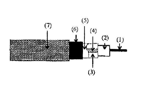
Turning first to Figure 1, a center conductor 1
is surrounded by a dielectric material 2. This
dielectric material 2 is in turn surrounded by gapped
foil 3 which can be a metallic laminate such as aluminum
and Mylar~ . A drain braid 4 is preferably included to
provide power handling capability and to improve
connector crimping. The drain braid 4 is located
opposite to the gap in the foil 3. A flooding compound
5 surrounds the dielectric, metallic laminate and drain
CA 0220448~ 1997-0~-0~
braid assembly to reduce damage to the cable in the
event of moisture penetrating the jacket through any
holes caused by accidental damage to the external
jackets 6 and 7.
S Semi-conductive polyethylene jacket 6 surrounds
the cable assembly. The purpose and exact properties of
the semi-conductive jacket 6 is to promote inductive
coupling as o~po~~~ to capacitive coupling between
transmit and receive cables. This is further discussed
below. Jacket 7 is a second high density polyethylene
protective jacket. This second high density
polyethylene jacket protects the cable against
incidental damage which could occur when the cable is
buried.
lS The semi-conductive jacket 6 serves two
purposes. First and foremost, this jacket promotes
inductive coupling between transmit and receive cables.
Second, this jacket provides some degree of protection
to the cable. This jacket can be replaced with a strip
of conductive material which surrounds the cable or
simply covers the gap in the foil 3 in which case
inductive coupling is still promoted but the protective
aspect is only provided by the high density polyethylene
protective jacket.
The value of the conductivity chosen for the
semi-conductive jacket 6 is critical to the invention.
The conductivity must ensure that the inductive coupling
is much greater than the capacitive coupling. At the
same time the conductivity must not be so high as to
reduce the inductive coupling and in order to accomplish
this the thickness of the jacket must be much less than
a skin depth at the operating frequency of the cable,
e.g. 40.68 MHz. These two factors set a range of
conductivities for which the sensor will work.
CA 0220448~ 1997-0~-0~
To address the first condition, the jacket 6
must be conductive enough to ensure that inductive
coupling is at least an order of magnitude greater than
capacitive coupling. The conductive jacket reduces
S inductive and capacitive coupling resulting in
inductive and capacitive insertion losses. The
insertion losses are determined by the following
equations.
lo Inductive Insertion Loss=2010g(1+jw~/K1) Equation [1]
Capacitive Insertion Loss=20log(1+j~/wK2) Equation [2]
where w=2~f, and f is the operating frequency
and ~ is the surface conductivity given by
~ = jacket thickness/volume resistivity of
the jacket
K1 and K2 are constants.
Figure 2 illustrates how the inductive and
capacitive coupling vary as jacket conductivity is
increased.
Note that the plotted range of volume
conductivity for the jacket is 0 to 4 S/m (Siemens per
meter). For values of volume conductivity greater than
1 S/m the inductive coupling is an order of magnitude
greater than the capacitive coupling as desired.
Next, the skin depth is calculated for the
conductive jacket, where
skin depth ~ = Sqrt(1/~f~)
Skin depth is plotted in Figure 3 vs. volume
conductivity ~.
It is desirable to make the skin depth much
greater than the jacket 6 thickness, for example a skin
depth at least 10 times greater than the jacket
thickness ensures that the signal is not attenuated by
the jacket. For a practical jacket thickness in the
CA 0220448~ 1997-0~-0~
range of 0.5 mm to 2 mm the skin depth must be greater
than 0.02 meters. The line in Figure 3 represents a
skin depth of 0.02 meters and-corresponds to a volume
conductivity of less than 15 S/m.
The range for practical values of volume
conductivity has now been set as:
1 S/m<Volume Conductivity < 15 S/m
It has been found that a semi-conductive
polyethylene jacket with a volume conductivity between
1 S/m and 15 S/m results in an excellent sensor cable
design.
A person understanding this invention may now
conceive of alternative structures and embodiments or
variations of the above. All those which fall within
the scope of the claims appended hereto are considered
to be part of the present invention.