Note: Descriptions are shown in the official language in which they were submitted.
CA 02204679 2000-OS-09
-1-
Self Testing Transceiver
Field of the Invention
The present invention relates generally to the field of radio frequency
transceivers and more particularly to a radio transceiver incorporating self
testing
capabilities.
Background of the Invention
One application for the use of Radio Frequency (RF) transceivers is to
transmit and receive RF signals for radio ports used in wireless
communications systems.
Presently, these radio frequency transceivers adapted for radio port use
within a wireless
communication system are not integrated units with respect to the performance
of certain
important functions. For instance, vital functions, such as self testing of
the transceiver,
are performed by various other external hardware components. Moreover, these
other
external components may be utilized to measure those radio channels in use by
other
nearby radio ports to assist in neighbor list construction of a radio port.
This reliance on
external components used in connection with present day transceivers leads to
higher
design costs due to the increased complexity of an interface between the
transceiver and
the external components and the inclusion of the external components
themselves. Such
a design may also increase the chances for radio port failure leading to
higher
maintenance costs.
Accordingly, there is a need for a fully integrated transceiver unit which
performs vital transceiver functions such as self testing and measuring active
radio
channels from other radio transceivers internally without reliance on other
external
components.
Summary of the Invention
In accordance with one aspect of the present invention there is provided an
integrated radio frequency transceiver apparatus adapted for use with a radio
port utilized
for communication within a wireless communication system, comprising: a
transmitter
operable for transmitting radio frequencies within a given frequency band; a
diversity
receiver having first and second receiver paths for receiving radio
frequencies within a
given frequency band, said transmitter being operable to transmit a self test
signal for
CA 02204679 2000-OS-09
-2-
receipt over at least one of said first and second receiver paths in response
to a self test
command, wherein a receipt of said self test signal from said at least one
receiver path
verifies proper operation of said transmitter and said at least one receiver
path, said first
receiver path receiving communications signals intended for said radio port
and said
second receiver path receiving communications signals transmitted from
transceivers of
other radio ports whereby a neighbor of said other radio ports may be
maintained based
on reception of said communication signals for other radio ports.
In accordance with another aspect of the present invention there is
provided an integrated radio frequency transceiver apparatus adapted for use
with a radio
I O port utilized for communications within a wireless communication system,
comprising: a
transmitter operable for transmitting radio frequencies within a given
frequency band; a
diversity receiver for receiving radio frequencies within a given frequency
band, said
transmitter being operable to transmit a self test signal for receipt at a
first receiver path
therein in response to a self test command, wherein a receipt of said test
signal verifies
proper operation of said transmitter and said receiver path; wherein said
diversity receiver
includes a second receiver path; wherein said first receiver path is for
receiving
communications signals intended for said radio port and said second receiver
path is for
receiving communications signals transmitted from transceivers of other radio
ports,
whereby a neighbor listing of other radio ports may be maintained based on
reception of
said communications signals for other radio ports.
In accordance with an illustrative embodiment of the present invention,
there is disclosed an integrated radio frequency transceiver comprising a
diversity
receiver and transmitter capable of performing a self test operation to
determine if the
receiver and transmitter paths are properly operational. The diversity
receiver includes
two receiver paths, a first path for receiving communications having a
permitted
bandpass, and a second receiver path for receiving radio signals from other
radio
frequency transceivers.
In an embodiment, the transmitter includes a quadrature modulator
adapted to receive local oscillator signals from a frequency synthesizer and
an
intermediate frequency synthesizer for generating proper transmission
frequencies. The
transmit path of the transmitter is duplexed via a bandpass filter with the
second receiver
CA 02204679 2000-OS-09
-2a-
path. A frequency synthesizer also supplies a local oscillator signal for a
mixing process
in the first receiver path. The first receiver path, which includes two
parallel bandpass
paths for receiving two frequency ranges, also receives a local oscillator
signal from the
frequency synthesizer for mixing with an incoming signal.
In an embodiment, for self testing purposes, the transmitter is adapted to
transmit a test signal which is routed by an internal switch to each of the
receiver paths.
An accurate reception of the test signal indicates properly operational
transmitter and
receiver paths. The second alternate receiver path, permits the radio
frequency
transceiver to detect radio signals from other radio frequency transceivers in
the wireless
communications system to maintain a list of active radio frequency
transceivers.
Brief Description of the Drawings
A more complete understanding of the present invention may be obtained from
consideration of the following description in conjunction with the drawings in
which:
FIG. 1 is a schematic block diagram showing one exemplary embodiment of an
intelligent radio port according to the present invention; and
FIG. 2 is a schematic block diagram of one exemplary embodiment of an
integrated transceiver module according to the present invention.
Detailed Description
Referring now to FIG. 1 there is shown a schematic block diagram of an
Intelligent Radio Port (IRP) unit module 10 in accordance with the present
invention. As
shown, the IRP unit includes a transceiver module 12 which is coupled to a
digital control
module 14. As would be understood by a person skilled in the art, in the shown
embodiment the transceiver module 12 is a single board transceiver that is a
part of the
Intelligent Radio Port (IRP) unit 10. The primary function of the transceiver
module 12
is to transmit and receive digitally modulated radio frequency (RF) control
signals and
information signals to and from mobile wireless communications devices. As
will be
explained, the transceiver has built-in test circuitry in order to test itself
in response to
signals generated from the digital control module 14. In addition, the
transceiver 12 is
capable of detecting radio frequency interference signatures from other
intelligent radio
ports (IRPs) i.e., sniffing, to thereby construct a neighbor list of these
nearby radio ports.
CA 02204679 2000-OS-09
-2b-
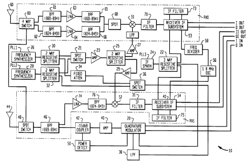
Referring to FIG. 2, the transceiver 12 is shown as an RF circuit module
that is part of an intelligent radio port of a wireless communications system.
In one
preferred embodiment, the transceiver transmits in the 869 to 894 MHz and can
CA 02204679 1997-OS-07
-3-
receive in either the 824 to 849 MHz band or 869 to 894 MHz band, however as
would be understood by a person skilled in the art, other bands may also be
utilized.
The operational capabilities of the transceiver enable the device to perform
in the
following functional modes: transmitter, diversity receiver, synthesizer, self-
test,
and sniffing mode, each of which modes will be discussed in greater detail
herein.
As set forth herein, the present description addresses only the radio
frequency signal processing aspect of the invention, as performed by the
transceiver
12. The digital control portion of the transceiver is provided by the digital
control
module (shown in FIG. 1 ), which is adapted to interface with the transceiver
module
12, as would be understood by a person skilled in the art. All signals except
the two
RF signals directly interface to the digital control module board.
Referring still to FIG. 2, the transmitter portion of the present invention
transceiver includes a quadrature modulator 20 which operates for example at
5.0
volts and produces a power output of approximately -3 dBm (decibels below 1
milliwatt). Quadrature modulation, i.e., the modulation of two Garner
components
90 degrees apart in phase by separate modulating functions, is well known to
those
skilled in the art. In the context of the present invention, such modulation
signals are
referred to as I ~ and Q IN signals for transmission operations and I o~ 1I 1
p~ and
Q o~ /Q 10~ signals for receive operations. The quadrature modulator 20 of the
present invention includes a built in power control wherein output power can
be
attenuated by approximately 50 dB. A complementary metal oxide
semiconductor/transistor transistor logic (CMOS/TT'I,) compatible input allows
the
device to go into power down mode when less than 10 micro-amps supply current
is
consumed. The quadrature modulator of the present invention can be found, for
example, in a single chip integrated circuit package model No. W2011 from AT&T
Corp.
In the shown embodiment of FIG. 2, the quadrature modulator 20 is a
direct conversion modulator with a built in offset mixer which prevents an
external
voltage controlled oscillator (VCO) from being pulled down by a large transmit
signal. The transmitter requires low level local oscillator (LO) signals to
eliminate
the use of an amplifier on the synthesizers. The transmitter receives one LO
signal at
82.2 MHz, via a 3-way splitter 22, from an intermediate frequency (IF)
synthesizer
24. The transmitter also receives another LO signal at 745-770 MHz or 787-811
MHz from agile frequency synthesizers 26, 28 based on the transmit frequency
thereby enabling outputs of the upper sideband to produce the desired
frequency. As
can be seen, the LO signals from the agile synthesizers 26, 28 arrive via
resistive
CA 02204679 1997-OS-07
-4-
splitters 30, 32 a fixed attenuator 34, SPDT switch 36 and a low pass filter
38. The
use of frequency synthesizers, which provide multiple frequency outputs, are
well
known to those skilled in the art. As would be understood, the agile frequency
synthesizers 26, 28 utilized herein, may be programmed and controlled by a
processor, for example, a microprocessor (not shown), to achieve the desired
LO
signals.
In one preferred embodiment of the present invention, the output from
the quadrature modulator 20 is input to the first stage of an amplifier 40
which boosts
the output signal by a given amount, e.g., l8dB. The output of this amplifier
40
enters a final power amplifier stage which adds another 7dB of gain to this
signal.
The output of the amplifier 40 next enters a -lSdB directional coupler 42 to
monitor
the power output to antenna 44. That is, after traveling through a bandpass
filter
(BPF~ duplexer 46 and SPDT switch 48, the Im/Q~ processed power signal is
directed out to the antenna 44 to be radiated. The SPDT switch 48 directs the
RF
power to the antenna 44 or other receiver paths for loopback tests as will be
described.
The intelligent radio ports used with the present invention integrated
transceiver 12 require the transmit power to be reduced in 4 dB steps from the
maximum rated transmit power the transceiver can transmit. To achieve a flat
characteristic independent of the gain spread in the amplifier stages, a power
leveling
loop, including power detector 50, external to the amplifier 40 is used. The
output of
the transmitter is adjusted by changing the control voltage to a gain control
input of
the transmitter. A pulse width modulation (PWM) signal, from a microcontroller
within the power detector, is low pass filtered to produce such a DC control
signal.
The transmitter can then be calibrated by using an external power meter to
find a
corresponding PWM number for each power level. A problem, however, is that
with
small variations in gain or load impedance, the power output can fluctuate as
well.
Also if the antenna 44 is accidentally removed with the unit in operation,
reverse
power may damage the unit. To address this problem, the power feedback loop
fed
into the -15 dB directional coupler 42 is adapted to sense the reverse power
and
rectify it. This signal is, in effect, added to the DC control signal output
from the
microcontroller. Accordingly, the loop will settle such that the output of the
detector
diode in the directional coupler 42 will be equal to the reference level. The
reference
level is then derived directly from the microcontroller and is set according
to the
required output power.
CA 02204679 1997-11-27
-5-
As would be understood, one must be careful to recognize that for the
self test purposes the transmitter transmits at 824-896 MHz, but the input to
the
bandpass filter (BPF) duplexer 46 accepts frequencies only from 869-894 MHz,
which
causes a loss of signal that could be as high as 60 dB. Therefore, for each
transceiver
unit calibration the exact signal arriving at the receiver must be found.
Also, the
channel used for making the self test should preferably be the channel not
used by the
mobile wireless communication devices.
Regarding the diversity receive function of the transceiver 12, it would be
understood that the receiver is to receive digitally modulated RF control and
information signals from mobile wireless communication devices and deliver
baseband
signals to a baseband processing unit. The receiver handles signals from -
lSdBm to
-102dBm or 87dBm of dynamic range. The receiver employs a double heterodyne
approach in each of the receive channels, i.e. two mixing processes, one at
mixer 51, 52
and another at the receiver IF subsystems 53, 54, respectively. Two
intermediate
frequencies are used, one at 82.2 MHz from the agile frequency synthesizers
26, 28 and
the IF synthesizer 24, and another at 455 kHz. The intermediate frequencies
from the
agile frequency synthesizers follow paths through the resistive sputters 30,
32 to
switch 21, to amplifier 23 to sputter 25 through amplifiers 27, 29 to either
mixer 51 or
mixer 52, respectively. The local oscillator source for the 455 kHz frequency
is derived
from a crystal oscillator 56 at 1.82 MHz, which is frequency divided by four
at
frequency divider 58 prior to input at the receiver IF subsystems.
The diversity receiver consists of two identical receivers, a first receiver
RXO and second receiver RX1. Both RXO and RX1 include RF amplification,
downconversion, IF bandpass filtering, IF amplification, gain control,
demodulation and
baseband circuits. As can be seen, both the RXO and RX1 receiver, include like
components. The RXO path, specifically, includes antenna 60, BPF 61 to LNA 63
to
BPF 65 or BPF 62 to LNA 64 to BPF 66, SPDT switch 68, MIXER 51, IF Filter 70
to
Receiver IF Subsystem 53 in conjunction with IF filter 73, to provide IouT and
QouT
signals. The RX1 Path, specifically, includes antenna 44, SPDT switch 48, BPF
duplexer 46, LNA 74, BPF 76, Mixer 52, IF Filter 31 to Receiver IF Subsystem
54 in
conjunction with IF Filter 79, to provide IlouT and QlouT signals.
CA 02204679 1997-11-27
- Sa -
Regarding the RXO receiver, the RF amplification circuit includes a 4-way
switch 80 which can connect the received signal to the appropriate receive
path
bandpass filter (BPF), i.e., 869-894 (MHz) or 824-849 (MHz), respectively. The
CA 02204679 1997-OS-07
-6-
switch 80 can also route a self-test signal from the transmitter to the 869-
894 MHz
bandpass filter 61. These signals, amplified by the low noise amplifier (LNA)
64
which has a typical noise figure of about 3dB, and the LNA 63 which has a
noise
figure of about 2.5 dB, are routed to the mixer 51 by the SPDT switch 68. The
LNA
64 has a 1dB compression point of 21 dBm to address high level band B signals
without saturating the amplifier, as would be understood by a person skilled
in the
art.
The down converter circuit of the RXO receiver includes a double
balanced mixer 51 which combines the incoming receive signals from the RF
amplification circuit with an agile LO frequency to produce the first IF at
82.2 MHz.
A second mixer in the IF subsystem 53 combines the first IF at 82.2 MHz with
an
82.2 MHz LO frequency from IF Synthesizer 24 to produce a third IF at 455 kHz.
Finally this 455 kHz signal is mixed with a fixed 455 kHz LO to produce Iout
an
Qout signals.
The IF bandpass filter 70 of the RXO receiver provides the channel
separation function for the receiver. In the shown embodiment, the 3 dB
bandwidth
of the filter is 30 kHz. As would be understood by a person skilled in the
art, the
filter 70 passes the tuned channel and rejects all other channels. A first IF
filter 70 is
an 82.2 MHz surface acoustic wave filter and requires input /output matching
to 50
ohms. The other IF bandpass filter 73 is at 455 kHz with a 3 dB bandwidth of
28 kHz
and 20 kHz respectively. This filter 73 is preferably a ceramic filter with
low group
delay response, the nominal impedance being 1000 ohms to 1500 ohms.
The receiver IF subsystem 53 is a low power IF subsystem for operation
at IF frequencies as high as 500 MHz and second IF frequencies as high as 22
MHz.
The subsystem 53, preferably includes a mixer, IF amplifiers, I and Q
demodulators,
a phase locked quadrature oscillator, an automatic gain control (AGC)
detector, and
a biasing system with external power down, where in one preferred embodiment
the
subsystem is an AD607 single chip IC from Analog Devices, Inc. The IF
subsystem
includes a low noise high intercept input mixer that is a doubly balanced
Gilbert-Cell
type and operates linearly for RF inputs spanning -102 to -15 dBm. The mixer
section also includes a local oscillator preamplifier, which lowers the drive
to -16
dBm. The single sided IF output can directly drive a bandpass filter with an
impedance of 200 ohm or greater. A gain control input can serve as either
manual
gain input or an automatic gain control voltage-based radio signal strength
indicator
(RSSI) output.
CA 02204679 1997-11-27
_7_
The diversity receiver path RX 1 is similar to receive path RXO, except
for the 2-way SPDT 48 switch that can route the transmit signal to either the
antenna 44 or to the RXO receiver path for a self-test. The BPF based duplexer
46
provides isolation between the transmit and receive paths.
As shown in FIG. 2, the synthesizer functional group of the present
invention transceiver 12 consists of an agile IF synthesizer 24 providing an
82.2
MHz LO source, a fixed 1.82 MHz crystal oscillator 56 which is divided by four
to
produce the 455 kHz signal and two frequency agile synthesizers 26 and 28. All
three synthesizers 24, 26, and 28 are programmed and controlled by a
microprocessor (not shown), so that the outputs from the frequency
synthesizers are
coherently locked to a reference frequency of 15 MHz. The chip used for phase
locked loop (PLL) operation is preferably an LMX 2332 from National
Semiconductor Corp. which has dual synthesizers including prescalers. Each
chip is
used to generate one RF and one IF local oscillator signal. Since the
transceiver has
to transmit at two different bands and receive at two different bands. The
number of
PLLs required will be at least four if a direct upconversion transmitter is
used. In the
shown embodiment an offset transmitter is used so that only two RF LOs are
required.
As has been discussed, transceiver 12 of the present invention may
operate in a self-test mode, in which the receiver essentially tests itself on
command
from a central processing unit on the digital control module to find any
failed
components in the transmit or receive path. The transmitter transmits a test
signal,
for instance a specially encoded message, from 824-849 MHz which is routed by
the
SPDT switch 48 to both the receivers RXO and RX1. A detection by the
processing
unit of a successful reception of the test signal at a separate port of the
digital control
module for each receiver indicates proper operating transmit and receive paths
in the
transceiver 12. Although the duplexer filter 46 at the transmit output is from
869-894 MHz, the filter will still pass the test signal with about 60 dB of
attenuation,
sufficient for test purposes. Another unique feature of the present invention
is that
the transmit signal is generated from heterodyning the receive local
oscillator with
the 82.2 MHz IF signal which in turn eliminates the use of two synthesizers.
The present invention transceiver may also operate in a sniffing mode to
detect radio interference signatures from other intelligent radio ports
(IRPs). The
SPDT switch 48 is operable to route RF transmissions received from other IRPs
to
the alternate receive path RX1. Based on this received signal at the control
module
each IRP maintains a list of active IRPs in the neighborhood which is stored
in
CA 02204679 1997-OS-07
_g_
memory in the control module. Since the signals from the other IRPs are not
going
to be very large a low noise amplifier 74 used in this path can have a low 1dB
compression point, therefore, an appropriate low noise amplifier is used.
From the above, it should be understood that the embodiments
described, in regard to the drawings, are merely exemplary and that a person
skilled
in the art may make variations and modifications to the shown embodiments
without
departing from the spirit and scope of the invention. All such variations and
modifications are intended to be included within the scope of the invention as
defined in the appended claims.