Note: Descriptions are shown in the official language in which they were submitted.
CA 02204798 1997-0~-08
Specification
Title of the Invention
ATM Switch
Background of the Invention
The present invention is used for ATM
(Asynchronous Transfer Mode) communication. The present
invention relates to a technique of simplifying
connection of the internal links of an ATM switch. The
present invention also relates to a technique of
constituting an ATM switch using an optical device. The
present invention also relates to a technique of coping
with traffic localization.
Figs. 16 to 18 explain a conventional ATM
switch. Fig. 16 shows the arrangement of a 4 x 4 (m
inputs and n outputs are represented by "m x n") basic
switch. Fig. 17 shows the detailed arrangement of a
cross point in the basic switch. Fig. 18 shows the
arrangement of a 16 x 16 ATM switch using eight 4 x 4
basic switches. The ATM switch is described in detail
in reference "Illustrated standard ATM textbook, ASCII
Shuppansha".
The arrangement of the basic switch will be
described with reference to Figs. 16 and 17. An input
buffer type basic switch will be described below. This
basic switch comprises input buffers 51-1 to 51-4 for
temporarily storing arriving cells, a controller 52 for
CA 02204798 1997-0~-08
controlling the congestion of cells, cross points 53 for
transferring ATM cells output from the input buffers
51-1 to 51-4 to desired output ports, and output
highways 54-1 to 54-4 to which ATM cells are
transferred. The controller 52 communicates with the
respective input buffers 51-1 to 51-4 to permit cell
transmission so as not to transfer the cells from the
input buffers 51-1 to 51-4 to the same one of the output
highways 54-1 to 54-4. The cross point 53 has an
address filter AF, as shown in Fig. 17, and transfers an
input cell to the corresponding one of the output
highways 54-1 to 54-4 on the basis of the information in
the header of the cell.
The conventional ATM switch is constituted
using a plurality of basic switches shown in Figs. 16
and 17. Fig. 18 shows a 16 x 16 ATM switch constituted
using eight 4 x 4 basic switches 71 to 78. The basic
switches 71 to 74 are individually connected to the
basic switches 75 to 78 through links so that a cell
from an arbitrary input line can be output to an
arbitrary output line.
When the ATM switch is to be constituted using
a plurality of basic switches, a number of links are
required to mutually connect the respective basic
switches. In addition, wires for connection are
intertwined with each other to result in a complex
structure. In the example shown in Fig. 18, 16 links
CA 02204798 1997-0~-08
are necessary. An actual large-scale ATM switch uses
several ten or several hundred basic switches, and the
number of links therebetween is enormous.
The links are constituted using optical
fibers. The process of connecting the wires requires a
long time. In addition, the check process for
preventing erroneous interconnection increases the
apparatus cost and the work time. Every time the number
of basic switches is increased/decreased,
interconnections between the wires must be changed for
all the basic switches, so the degree of freedom in
increasing/decreasing the number of basic switches is
low.
When the traffics localize in routes from the
basic switch 71 to the basic switch 75 and from the
basic switch 72 to the basic switch 76, the links
connecting these switches congest. This situation is
shown in Fig. 19. Fig. 19 shows the congestion
situation of the 16 x 16 ATM switch. This largely
degrades the throughput of the switch.
Summary of the Invention
It is the principal object of the present
invention to provide an ATM switch capable of flexibly
coping with an increase/decrease in the number of
input/output lines.
It is another object of the present invention
to provide an ATM switch capable of solving the
CA 02204798 1997-0~-08
conventional complex link connection to reduce the
quantity of hardware.
It is still another object of the present
invention to provide an ATM switch capable of solving
traffic localization generated in the respective lines.
It is still another object of the present
invention to provide an ATM switch applicable to a
large-scale ATM switch structure.
In order to achieve the above objects of the
present invention, there is provided an ATM switch for
distributing cells arriving from a plurallty of input
lines to a plurality of output lines, comprising a
plurality of input line corresponding units each
connected to the plurality of input lines, a plurality
of output line corresponding units each connected to the
plurality of output lines, and wavelength shifting
means, arranged between the input line corresponding
units and the output line corresponding units, for
shifting optical signals having different wavelengths
included in a plurality of wavelength-multiplexed
optical signals arriving from the input line
corresponding units and outputting the
wavelength-multiplexed optical signals, wherein each of
the input line corresponding units includes an
input-side basic switch for distributing N (N is a
positive integer) cells which are respectively input to
a plurality of input ports to N lines, electro-optic
CA 02204798 1997-0~-08
conversion means for converting the cells distributed to
the N lines into optical signals having different
wavelengths in units of lines, and a multiplexer for
multiplexing the optical signals converted in units of
lines into one wavelength-multiplexed optical signal,
and each of the output line corresponding units includes
a demultiplexer for demultiplexing in units of
wavelengths the wavelength-multiplexed optical signal
obtained by wavelength-multiplexing the optical signals
having N wavelengths, opto-electric conversion means for
converting outputs from the demultiplexer into
electrical signals, respectively, and an output-side
basic switch for distributing the cells converted into
the electrical signals to a plurality of output ports.
The present invention is characterized in that
basic switches are connected through wavelength
multiplexing links such that the basic switches are
connected through wavelength shifting means for
distributing signals on the respective multiplexing
links in units of wavelengths. The present invention is
different from the prior art in that the number of links
is reduced by wavelength multiplexing, the output-side
basic switch is selected in units of wavelengths, and
one output-side basic switch is connected to the
respective input-side basic switches through links with
different wavelengths.
-- 5
CA 02204798 1997-0~-08
In addition, the present invention is
characterized in that some output ports of the output
line corresponding units are connected to the
corresponding input ports of the input line
corresponding units, respectively, or some output ports
of a certain input line corresponding unit are connected
to input ports of another input line corresponding unit
such that bypass routes for avoiding congestion can be
set.
More specifically, the first gist of the
present invention is an ATM switch for distributing
cells arriving from a plurality of input lines to a
plurality of output lines.
According to the present invention, there is
provided an ATM switch comprising a plurality of input
line corresponding units each connected to the plurality
of input lines, a plurality of output line corresponding
units each connected to the plurality of output lines,
each of the input line corresponding units including an
input-side basic switch for distributing cells which are
respectively input to a plurality of input ports to N
lines, electro-optic conversion means for converting the
cells distributed to the N lines into optical signals
having different wavelengths in units of lines, and a
multiplexer for multiplexing the optical signals
converted in units of lines into one
wavelength-multiplexed optical signal, and each of the
CA 02204798 1997-0~-08
output line corresponding units including a
demultlplexer for demultiplexing in units of wavelengths
the wavelength-multiplexed optical signal obtained by
wavelength-multiplexing the optical signals having N
wavelengths, opto-electric conversion means for
converting outputs from the demultiplexer into
electrical signals, respectively, and an output-side
basic switch for distributing the cells converted into
the electrical signals to a plurality of output ports,
and wavelength shifting means, arranged between the
input line corresponding units and the output line
corresponding units, for shifting the optical signals
having different wavelengths included in a plurality of
wavelength-multiplexed optical signals arriving from the
input line corresponding units and outputting the
wavelength-multiplexed optical signals.
Preferably, the wavelength shifting means
includes a barrel shifter which distributes an optical
signal having a pth (p = 0, 1, 2,..., (N - 1))
wavelength in an nth (n = 0, 1, 2,..., (the number of
input line corresponding units - 1))
wavelength-multiplexed optical signal to the (n + p)th
output and distributes the optical signal to the output
of an ordinal number obtained by subtracting the number
of output line corresponding units from (n + p) when n +
p is equal to or larger than the number of output line
corresponding units.
-- 7
CA 02204798 1997-0~-08
With this arrangement, the cells arriving from
the plurality of input lines can be distributed to the
output lines determined in units of wavelengths. At
this time, use of the wavelength shifting means such as
S a barrel shifter allows to omit complex interconnections
and increases the degree of freedom in
increasing/decreasing the number of lines. More
specifically, one output-side basic switch is connected
to the respective input-side basic switches through
links with different wavelengths when viewed from this
output-side basic switch.
The number of input line corresponding units
can be made equal to that of output line corresponding
units. The numbers of input line corresponding units or
output line corresponding units can be arbitrarily set.
For this reason, an ATM switch having a high degree of
freedom in design can be realized.
Wavelength multiplexing links are preferably
arranged between the output terminals of the
multiplexers and the wavelength shifting means and
between the wavelength shifting means and the input
terminals of the demultiplexers. With this arrangement,
the number of links input/output to/from the wavelength
shifting means can be reduced, so that an ATM switch
which can omit complex interconnections can be realized.
The number of basic switches can be easily changed by
increasing/decreasing the number of links input/output
CA 02204798 1997-0~-08
to/from the wavelength shifting means. More
speciflcally, the number of basic switches can be easily
changed by increasing/decreasing not the number of
outputs of the basic switches but the number of links
input/output to/from the wavelength shifting means in
correspondence with the number of basic switches
themselves.
At least some input ports of the plurality of
input line corresponding units may be connected to lines
from any routes from other input line corresponding
units to the plurality of output line corresponding
units. With this arrangement, a plurality of routes via
feedback routes can be selected as a route for
transferring a cell from a certain input line to a
certain output line. Therefore, in case of traffic
localization, a bypass route can be formed to cope with
the traffic localization.
To obtain simple and regular interconnections,
at least some output ports of each output-side basic
switch are preferably connected to input ports of an
input-side basic switch corresponding to the output-side
basic switch. Alternatively, at least some output ports
of each input-side basic switch may be connected to
input ports of the input-side basic switch of another
input line corresponding unit.
Alternatively, for a combination of at least
one input line corresponding unit and an output line
CA 02204798 1997-0~-08
corresponding unit corresponding to this input line
corresponding unit, the output ports of the output line
corresponding unit may be connected to the input ports
of the input line corresponding unit. The combination
of an input line corresponding unit and an output line
corresponding unit corresponding to this input line
corresponding unit is specialized to form bypass routes,
and the remaining input line corresponding units and
output line corresponding units can have the basic
arrangement. With this arrangement, the degree of
freedom in increasing/decreasing the number of
input/output lines can be increased.
Electro-optic conversion means for converting
cells into optical signals having different wavelengths
in units of inputs and a multiplexer for multiplexing
the optical signals converted in units of inputs into
one wavelength-multiplexed optical signal may be
arranged. This multiplexer is connected to the input
side of the wavelength shifting means. The plurality of
output line corresponding units may include at least one
output line corresponding unit whose output ports are
connected to the input ports of the electro-optic
converters. With this arrangement, in the above
specialized arrangement, the arrangement corresponding
to the input line corresponding units can be simplified.
-- 10 --
CA 02204798 1997-0~-08
The second gist of the present invention is a
large-scale ATM switch in which the above ATM switches
are multiple-connected.
Brief Description of the Drawings
Fig. 1 is a block diagram of an ATM switch
according to the first embodiment of the present
invention;
Fig. 2 is a view showing the situation of
optical signal distribution by a barrel shifter;
Fig. 3 is a view showing the concept of an
arrayed-waveguide grating;
Fig. 4 is a view showing the situation of
input/output of the barrel shifter;
. Fig. 5 is a block diagram of an ATM switch
according to the second embodiment of the present
invention;
Fig. 6 is a view for explaining an operation
performed when traffic localization occurs in the ATM
switch according to the second embodiment of the present
invention;
Fig. 7 is a block diagram of an ATM switch
according to the third embodiment of the present
invention;
Fig. 8 is a view for explaining an operation
performed when traffic localization occurs in the ATM
switch according to the third embodiment of the present
invention;
CA 02204798 1997-0~-08
Fig. 9 is a block diagram of an ATM switch
accordlng to the fourth embodiment of the present
invention;
Fig. 10 is a view for explaining an operation
performed when traffic localization occurs in the ATM
switch according to the fourth embodiment of the present
invention;
Fig. 11 is a block diagram of an ATM switch
according to the fifth embodiment of the present
invention;
Fig. 12 is a view for explaining an operation
performed when traffic localization occurs in the ATM
switch according to the fifth embodiment of the present
lnvention;
Fig. 13 is a block diagram of the sixth
embodiment of the present invention;
Fig. 14 is a block diagram of the seventh
embodiment of the present invention;
Fig. 15 is a block diagram of a multiple ATM
switch according to the eight embodiment of the present
invention;
Fig. 16 is a view showing the arrangement of a
4 x 4 basic switch;
Fig. 17 is a view showing the detailed
arrangement of a cross point;
Fig. 18 is a view showing the arrangement of a
16 x 16 ATM switch using eight 4 x 4 basic switches; and
CA 02204798 1997-0~-08
Fig. 19 is a view showing the link congestion
situation.
Description of the Preferred Embodiments
(First Embodiment)
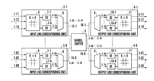
The arrangement of the first embodiment of the
present invention will be described below with reference
to Fig. 1. Fig. 1 shows the arrangement of an ATM
switch according to the first embodiment of the present
invention.
In the present invention, an ATM switch which
distributes arriving cells from 64 input lines to 64
output lines will be described.
The present invention has the following
characteristic features. The ATM switch comprises input
15 line corresponding units 2-1 to 2-8 (2-2 to 2-7 are not
illustrated) each connected to eight lines of a total of
64 input lines, and output line corresponding units 4-1
to 4-8 (4-2 to 4-7 are not illustrated) each connected
to eight lines of a total of 64 output lines. Each of
the input line corresponding units 2-1 to 2-8 includes
an 8 x 8 input-side basic switch 6 for distributing
cells input to eight input ports 1-11 to 1-18,..., or
1-81 to 1-88 to the eight lines, electro-optic
converters 7-1 to 7-8 for converting the cells
distributed to the eight lines into optical signals
having different wavelengths in units of lines, and a
multiplexer 8 for multiplexing the optical signals
- 13 -
CA 02204798 1997-0~-08
converted in units of lines into one
wavelength-multiplexed optical signal. Each of the
output line corresponding units 4-1 to 4-8 includes a
demultiplexer 9 for demultiplexing the
wavelength-multiplexed optical signal formed by
wavelength-multiplexing eight optical signals into
optical signals having wavelengths different from each
other, opto-electric converters 10-1 to 10-8 for
converting outputs from the demultiplexer 9 into
electrical signals, respectively, and an 8 x 8
output-side basic switch ll for distributing the cells
converted into the electrical signals to eight output
ports 5-11 to 5-18,..., or 5-81 to 5-88. A barrel
shifter 3 serving as a wavelength shifting means for
shifting the optical signals having different
wavelengths included in a plurality of
wavelength-multiplexed optical signals arriving from the
input line corresponding units 2-1 to 2-8 and outputting
the wavelength-multiplexed optical signals is arranged
between the input line corresponding units 2-1 to 2-8
and the output line corresponding units 4-1 to 4-8.
The barrel shifter 3 distributes an optical
signal having the pth (p = 0,..., N - 1) wavelength in
the nth (n = 0, 1,..., (the number of input line
corresponding units - 1)) wavelength-multiplexed optical
signal to the (n + p)th output. When n + p is equal to
or larger than the number of output line corresponding
- 14 -
CA 02204798 1997-0~-08
units, the optical signal is distributed to the output
of an ordinal number obtained by subtracting (the number
of output line corresponding units) from (n + p).
In the first embodiment of the present
invention, the number of the input line corresponding
units 2-1 to 2-8 equals that of the output line
corresponding units 4-1 to 4-8.
Wavelength multiplexing links 15-1 to 15-8 and
wavelength multiplexing links 16-1 to 16-8 are arranged
between the output terminals of the multiplexers 8 and
the barrel shifter 3 and between the barrel shifter 3
and the input terminals of the demultiplexers 9,
respectively.
. The electro-optic converters 7-1 to 7-8 output
optical signals having wavelengths Ao to 17,
respectively. Suffixes A to H are added to clarify the
input line corresponding units 2-1 to 2-8 in which the
optical signals are converted. More specifically, the
wavelengths of optical signals in the input line
corresponding unit 2-1 are represented by ;~OA to ;~7A~ and
the wavelengths of optical signals in the input line
corresponding unit 2-8 are represented by ~OH to A.7H.
The barrel shifter will be described with
reference to Fig. 2. Fig. 2 shows the situation of
optical signal distribution by the barrel shifter. As
shown in Fig. 2, a description will be made assuming two
input lines #0 and #1 and four output lines #0 to #3.
CA 02204798 1997-0~-08
Optical signals each having wavelengths AO to A3 are
transmitted to input lines #0 and #1, respectively.
Output lines #0, #1, #2, and #3 are set as output lines
of the optical signals having wavelengths AO~ A1~ AZ, and
5 A3 in input line #0, respectively. Output lines #1, #2,
#3, and #0 are set as output lines of the optical
signals having wavelengths AO, A1~ AZ, and A3 in input
line #1, respectively. Output line #1 is used to output
the wavelength Al of the optical signals transmitted
through input line #0. Output line #l is also used to
output the wavelength AO of the optical signals
transmitted through input line #1. In the ATM switch
shown in Fig. 1, a cell to be output to the output line
corresponding unit 4-1 may be input to the electro-optic
15 converter 7-1 for converting the cell into an optical
signal having the wavelength AOA- The cell input to the
electro-optic converter 7-1 is converted into the
optical signal having the wavelength AOA and input to the
barrel shifter 3 through the wavelength multiplexing
link 15-1. The cell is then output to the wavelength
multiplexing link 16-1 and arrives at the output line
corresponding unit 4-1.
The barrel shifter is a known technique. It
is not directly associated with the present invention,
and a detailed description thereof will be omitted. The
barrel shifter will be briefly described below
(reference: Hiroshi Takahashi et al.,
- 16 -
CA 02204798 1997-0~-08
"Polarization-insensitive arranged waveguide grating
wavelength multiplexer on silicon", OPTICS LETTERS,
Vol. 17, No. 7, April 1 1992, pp. 499-501.
The optical device usèd in the present
invention, i.e., the optical device called a barrel
shifter is one of optical devices generally called
"arrayed-waveguide gratings". Fig. 3 shows the concept
of the arrayed-waveguide grating. Normally, the
arrayed-waveguide grating is integrated on a substrate
together with input and output waveguides and two slab
waveguides each functioning as a collimator/condenser
lens, and manufactured as a multiplexer/demultiplexer.
As shown in Fig. 3, the arrayed-waveguide
grating is constituted by a plurality of waveguides
arranged at an equal interval and having different
lengths. The phase shift between the waveguides
generates the same dispersion properties as those of a
diffraction grating. Therefore, wavelength-multiplexed
light from the input waveguide is demultiplexed and
extracted from different output waveguides. This device
is used as a multiplexer in a reverse direction. The
slab waveguide has a sectorial shape whose center of
curvature is at the end of the input or output
waveguide. The slab waveguide also has a condenser
function, like a concave mirror, because the axis of the
waveguide of the arrayed-waveguide grating is directed
to the center of curvature. To reduce the connection
CA 02204798 1997-0~-08
loss, a tapered waveguide is generally inserted between
the channel waveguide and the slab waveguide, which
constitute the arrayed-waveguide grating.
A wavelength interval ~A as one of the most
important parameters of the multiplexer/demultiplexer
using the arrayed-waveguide grating is represented as
follows:
~A = ~x/(f-m/nx-d) ...(1)
m = (nc-~L)/Ao ...(2)
where ~L is the difference between a pitch d of the
arrayed-waveguide grating and the length of the
waveguides constituting the arrayed-waveguide grating, f
is the focal length (= radius of curvature) of the slab
waveguide, ~x is the interval of the input and output
waveguides, and nx is the effective refractive index of
the slab waveguide. The denominator (f-m/nx-d) on the
right-hand side of equation (1) represents a linear
dispersion and the proportional constant of the
relationship between the wavelength and the condensing
position, nc is the effective refractive index of the
waveguide, Ao is the center wavelength of the
arrayed-waveguide grating, i.e., the wavelength obtained
from the central output waveguide, and m is the degree
of diffraction of the arrayed-waveguide grating, i.e., a
numerical value representing the phase shift of light
between adjacent waveguides. As the value m becomes
large, the angular dispersion becomes large. For this
- 18 -
CA 02204798 1997-0~-08
reason, wavelengths having a small interval can be
multiplexed/demultiplexed (the wavelength resolving
power is high). For a conventional diffraction grating,
the pitch must be reduced to increase the resolving
power, though there is a process limitation. In the
arrayed-waveguide grating, the waveguide can be
elongated to increase the degree of diffraction, thereby
easily realizing a high resolving power. This is the
largest difference between the arrayed-waveguide grating
and the conventional diffraction grating.
As is represented by equation (2), since m is
an arbitrary integer, a plurality of center wavelengths
Ao are present in one arrayed-waveguide grating. For
example, when the optical path difference ~L = 126 ~m,
and nc = 1.45, Ao = 1548.3 nm for m = 118, and ~0 =
1535.3 nm for m = 119. That is, light components having
a plurality of wavelengths Ao including 1548.3 nm and
1535.3 nm are output from the central output port.
Therefore, a band usable without overlapping the
wavelengths is 13 nm. For wavelength division
multiplexing at a wavelength interval of 0.8 nm, the
m~Ximum number of wavelengths is "16". When the value m
increases, the wavelength resolving power increases.
However, the band usable without overlapping the
wavelengths becomes narrow, so the value m must be
carefully set.
-- 19 --
CA 02204798 1997-0~-08
The barrel shifter used in the present
invention is an arrayed-waveguide grating which
positively utilizes its nature (circulation properties)
that light components having the same wavelength are
repeatedly output in units of bands usable without
overlapping the wavelengths, as shown in Table 1.
Table 1
I/O 01 02 03 04 05
il Ao Al A2 A3 A4
i2 A4 Ao Al A2 A3
i3 A3 A4 Ao Al A2
i4 A2 A3 A4 Ao Al
i5 Al A2 A3 A4 Ao
Fig. 4 shows the situation of input/output of
the barrel shifter 3 shown in Fig. 1. One output-side
basic switch is connected to the respective input-side
basic switches through links with different wavelengths
when viewed from this output-side basic switch.
The operation of the first embodiment of the
present invention will be described next. Cells input
to the input line corresponding units 2-1 to 2-8 are
switched by the input-side basic switches 6. The output
line corresponding units 4-1 to 4-8 as destinations are
determined in accordance with output lines switched by
the input-side basic switches 6. For example, when one
of cells input to the input line corresponding unit 2-l
is to use the output line corresponding unit 4-1 as an
output line, the cell may be input to the electro-optic
- 20 -
CA 02204798 1997-0~-08
converter 7-1 for converting the cell into an optical
signal having the wavelength AOA- The cell input to the
electro-optic converter 7-1 is converted into the
optical signal having the wavelength AOA and input to the
barrel shifter 3 through the wavelength multiplexing
link 15-1 and arrives at the output line corresponding
unit 4-1 through the wavelength multiplexing link 16-1.
The operation of the input line corresponding
unit 2-1 will be described in more detail. Cells output
from the input-side basic switch 6 are converted into
optical signals having the wavelengths AOA to A7A by the
electro-optic converters 7-1 to 7-8, respectively.
These optical signals are multiplexed by the multiplexer
8 into one serial signal and output to the wavelength
multiplexing link 15-1. The barrel shifter 3
selectively distributes the optical signals having the
wavelengths AOA to A7A to the wavelength multiplexing
links 16-1 to 16-8. On the other hand, when attention
is paid to one wavelength multiplexing link, e.g., 16-1,
optical signals from the input line corresponding units
2-1 to 2-8 are wavelength-multiplexed and transferred to
the wavelength multiplexing link 16-1.
The demultiplexer 9 demultiplexes the
wavelength-multiplexed optical signal from the input
line corresponding units 2-1 to 2-8. The opto-electric
converters 10-1 to 10-8 convert the optical signals into
cells of electrical signals. The cells are output to
CA 02204798 1997-0~-08
the output lines by the output-side basic switch 11
through the desired output ports 5-11 to 5-18,
respectively.
In connection between the input port 1-12 of
the input-side basic switch 6 of the input line
corresponding unit 2-1 and the output port 5-14 of the
output-side basic switch 11 of the output line
corresponding unit 4-1, the electro-optic converter 7-1
at the uppermost stage is selected by the input-side
basic switch 6. The optical signal having the
wavelength~OA is transferred to the output line
corresponding unit 4-1 through the barrel shifter 3,
demultiplexed by the demultiplexer 9 to the output-side
basic switch 11, and connected to the output port 5-14
by the basic switch 11.
As described above, cells arriving from the
plurality of input lines can be distributed to the
output lines which are determined in units of
wavelengths. When the barrel shifter 3 is used, the
internal links of the ATM switch can be simplified.
When a plurality of ATM switches of the
present invention are connected, a large-scale ATM
switch having, e.g., three or five stages can be
constituted.
(Second Embodiment)
The arrangement of the second embodiment of
the present invention will be described with reference
CA 02204798 1997-0~-08
to Figs. 5 and 6. Fig. 5 shows an ATM switch according
to the second embodiment of the present invention. In
the second embodiment, output ports 5-11 to 5-18,....
5-81 to 5-88 of output-side basic switches 11 of output
line corresponding units 4-1 to 4-8 are connected to
input ports 1-11 to 1-18,..., 1-81 to 1-88 of input-side
basic switches 6 of input line corresponding units 2-1
to 2-8 through linès 12-1 to 12-8. With this
arrangement, when partial congestion occurs in the ATM
switch, a bypass route for avoiding the congested route
can be set.
Fig. 6 explains an operation performed when
traffic localization occurs in the ATM switch according
to the second embodiment of the present invention and
shows a case wherein the traffic of the input line
corresponding unit 2-1 concentrates to the output line
corresponding unit 4-1. To transfer a cell from the
input line corresponding unit 2-1 to the output line
corresponding unit 4-1, a wavelength AOA is selected, and
the cell is automatically transferred by a barrel
shifter 3. However, when the transfer rate of the input
ports 1-11 to 1-18,..., 1-81 to 1-88 is 1 Gb/s, traffics
of 8 Gb/s may localize between the input line
corresponding unit 2-1 and the output line corresponding
unit 4-1 at maximum. Assume that the throughput at
which a cell can be transferred via one wavelength of
wavelength multiplexing links 15-1 to 15-8 or 16-1 to
- 23 -
CA 02204798 1997-0~-08
16-8 is 1 Gb/s. When a cell is to be directly
transferred from the input line corresponding unit 2-1
to the output line corresponding unit 4-1, only cells of
1 Gb/s of the cells of 8 Gb/s can be transferred. The
remaining cells of 7 Gb/s are handled as a call loss.
To avoid this, a feedback route is used. In the example
shown in Fig. 6, in addition to a route A for directly
transferring a cell from the input line corresponding
unit 2-1 to the output line corresponding unit 4-1, a
route B is arranged to select A1A for some cells to be
transferred to the output line corresponding unit 4-1,
and transfer the cells to the output line corresponding
unit 4-2. The cell from the output line corresponding
unit 4-2 is fed back to the input line corresponding
unit 2-2 via the feedback loop and transferred from the
input line corresponding unit 2-2 to the output line
corresponding unit 4-1. Therefore, congestion between
the input line corresponding unit 2-1 and the output
line corresponding unit 4-1 can be avoided.
Although one bypass route has been exemplified
above, seven bypass routes can be additionally ensured
between the input line corresponding unit 2-1 and the
output line corresponding unit 4-1. Consequently, a
total of eight routes can be used. In addition, not one
but a plurality of feedback routes can be set between
the input line corresponding units 2-1 to 2-8 and the
output line corresponding units 4-1 to 4-8.
- 24 -
CA 02204798 1997-0~-08
(Third Embodiment)
The third embodiment of the present invention
will be described with reference to Figs. 7 and 8.
Fig. 7 shows an ATM switch according to the third
embodiment of the present invention. The third
embodiment of the present invention includes a circuit
in which each of input line corresponding units 2-1 to
2-8 has a 9 x 9 input-side basic switch 13 for
distributing cells input to nine input ports 1-11 to
1-19, 1-21 to 1-29,... , or 1-81 to 1-89, and one of the
output ports of each input-side basic switch 13 is
connected to the input port 1-19, 1-29,..., or 1-89 of
the corresponding one of the input line corresponding
units 2-1 to 2-8 without interposing electro-optic
lS converters 7-1 to 7-8.
According to the third embodiment, no bypass
route need be set for the subsequent paths. Only by
increasing the number of input/output ports of the
input-side basic switch 13 by one, an ATM switch having
a 64 x 64 arrangement can be constituted.
More specifically, in the third embodiment of
the present invention, eight input lines are connected
to each of the input line corresponding units 2-1 to
2-8, and eight output lines are connected to each of
output line corresponding units 4-1 to 4-8. Instead of
the 8 x 8 input-side basic switch 6 in the first and
second embodiments of the present invention, each of the
- 25 -
CA 02204798 1997-0~-08
input line corresponding units 2-1 to 2-8 has the 9 x 9
basic switch, i.e., the input-side basic switch 13 for
distributing cells input to the nine input ports to the
nine lines. Of these nine lines, eight lines are
connected to the electro-optic converters 7-1 to 7-8,
respectively, as in the first and second embodiments of
the present invention. The remaining one line of each
input-side basic switch 13 is connected such that the
line of the input-side basic switch 13 of the input line
corresponding unit 2-(8-k) (k = 1, 2,... , 8) is
connected to an input port of the input-slde basic
switch 13 of the input line corresponding unit
2-(8-(k+1)) (when k = 8, the input line corresponding
unit 2-1). The remaining arrangement in each of the
input line corresponding units 2-1 to 2-8, and the
arrangement of a barrel shifter 3 and the output line
corresponding units 4-1 to 4-8 are the same as those in
the first embodiment of the present invention.
Fig. 8 explains an operation performed when
traffic localization occurs in the ATM switch according
to the third embodiment of the present invention.
Assume that the traffic localizes between the input line
corresponding unit 2-1 and the output line corresponding
unit 4-1, as in the description of Fig. 6. In this
case, in addition to a route A for directly transferring
a cell from the input line corresponding unit 2-1 to the
output line corresponding unit 4-1, a route B is set.
- 26 -
CA 02204798 1997-0~-08
With this route B, some cells to be transferred to the
output line corresponding unit 4-1 are transferred to
the input line corresponding unit 2-2 by using the line
14-1, and ~7B iS selected to transfer the cells to the
output line corresponding unit 4-1. When traffics also
concentrate between the input line corresponding unit
2-2 and the output line corresponding unit 4-1, some
cells from the input line corresponding unit 2-1 can be
further transferred to the input line corresponding unit
2-3. With this arrangement, a plurality of routes can
be used to transfer cells from the input line
corresponding unit 2-1 to the output line corresponding
unit 4-1. In addition, not only one but a plurality of
routes can be set among the input line corresponding
units 2-1 to 2-8.
In the third embodiment of the present
invention, an arrangement which includes a regular wire
structure and can be easily practiced has been
described. However, the present invention can be
practiced even for another connection form. For
example, outputs from some opto-electric converters 10-k
of the output line corresponding units 4-1 to 4-8 can be
connected to the input line corresponding units 2-1 to
2-8. Alternatively, some outputs from the input-side
basic switch 13 can be connected to a common input line
corresponding unit 2-k.
- 27 -
CA 02204798 1997-0~-08
(Fourth Embodiment)
The fourth embodiment of the present invention
will be described with reference to Figs. 9 and 10.
Fig. 9 shows an ATM switch according to the fourth
embodiment of the present invention. In the fourth
embodiment of the present invention, output ports 5-81
to 5-88 of an output-side basic switch 11 of an output
line corresponding unit 4-8 are connected to input ports
1-81 to 1-88 of an input-side basic switch 6 of an input
line corresponding unit 2-8 through lines 18-1 to 18-8
constituting a feedback circuit, respectively, thereby
specializing the input line corresponding unit 2-8 and
the output line corresponding unit 4-8 to set bypass
routes.
According to the fourth embodiment of the
present invention, remaining input line corresponding
units 2-1 to 2-7 and output line corresponding units 4-1
to 4-7 can have the basic arrangement shown in the first
embodiment of the present invention. Therefore, the
input line corresponding units and output line
corresponding units can be easily increased/decreased.
Fig. 10 explains an operation performed when
traffic localization occurs in the ATM switch according
to the fourth embodiment of the present invention.
Assume that the traffics localize between the input line
corresponding unit 2-1 and the output line corresponding
unit 4-1, as in the description of Fig. 6. In this
- 28 -
CA 02204798 1997-0~-08
case, in addition to a route A for directly transferring
cells from the input line corresponding unit 2-1 to the
output line corresponding unit 4-1, a route B is set to
transfer some cells to be transferred to the output line
corresponding unit 4-1 to the output line corresponding
unit 4-8. The cells are further transferred to the
input line corresponding unit 2-8 and then transferred
from the input line corresponding unit 2-8 to the output
line corresponding unit 4-2. As described above, a
plurality of routes can be used between the input line
corresponding unit 2-1 and the output line corresponding
unit 4-1.
(Fifth Embodiment)
The fifth embodiment of the present invention
will be described with reference to Figs. 11 and 12.
Fig. 11 shows an ATM switch according to the fifth
embodiment of the present invention. In the fifth
embodiment of the present invention, a block without any
input-side basic switch 6 is arranged as an input line
corresponding unit 2-8', and output ports 5-81 to 5-88
of an output-side basic switch 11 of an output line
corresponding unit 4-8 are connected to the input
terminals of electro-optic converters 7-1 to 7-8 through
lines 18-1 to 18-8 constituting a feedback circuit,
respectively, thereby specializing the input line
corresponding unit 2-8' and the output line
corresponding unit 4-8 to set bypass routes.
- 29 -
CA 02204798 1997-0~-08
According to the fifth embodiment of the
present invention, remaining input line corresponding
units 2-1 to 2-7 and output line corresponding units 4-l
to 4-7 can have the basic arrangement shown in the first
embodiment of the present invention. Therefore, the
input line corresponding units and output line
corresponding units can be easily increased/decreased.
In addition, according to the fifth embodiment
of the present invention, the input line corresponding
unit 2-8' can have a simpler arrangement than that of
the fourth embodiment of the present invention. The
input line corresponding unit 2-8' has no input-side
basic switch 6. However, desired routes can be set on
the side of the output-side basic switch 11 of the
output line corresponding unit 4-8.
Fig. 12 explains an operation performed when
traffic localization occurs in the ATM switch according
to the fifth embodiment of the present invention.
Assume that the traffics localize between the input line
corresponding unit 2-1 and the output line corresponding
unit 4-1, as in the description of Fig. 6. In this
case, in addition to a route A for directly transferring
cells from the input line corresponding unit 2-1 to the
output line corresponding unit 4-1, a route B is set to
transfer some cells to be transferred to the output line
corresponding unit 4-1 to the output line corresponding
unit 4-8. The cells are further transferred to the
- 30 -
CA 02204798 1997-0~-08
input line corresponding unit 2-8' and then transferred
from the input line corresponding unit 2-8' to the
output line corresponding unit 4-2. As described above,
a plurality of routes can be used between the input line
corresponding unit 2-1 and the output line corresponding
unit 4-1.
(Sixth Embodiment)
The sixth embodiment of the present invention
will be described with reference to Fig. 13. Fig. 13
shows the sixth embodiment of the present invention. In
the sixth embodiment of the present invention, the
arrangement shown in the second embodiment of the
present invention is combined with that shown in the
third embodiment of the present invention.
When traffic localization occurs in the ATM
switch of the sixth embodiment of the present invention,
not only the bypass route shown in Fig. 6 but also that
shown in Fig. 8 can be set. With this arrangement, the
degree of freedom in setting the bypass route can be
increased.
(Seventh Embodiment)
The seventh embodiment of the present
invention will be described with reference to Fig. 14.
Fig. 14 shows the seventh embodiment of the present
invention. In the seventh embodiment of the present
invention, the arrangement shown in the third embodiment
- 31 -
CA 02204798 1997-0~-08
of the present invention is combined with that shown in
the fourth embodiment of the present invention.
When traffic localization occurs in the ATM
switch of the seventh embodiment of the present
invention, not only the bypass route shown in Fig. 6 but
also that shown in Fig. 10 can be set. With this
arrangement, the degree of freedom in setting the bypass
route can be increased.
The same description can apply to a
combination of the arrangement shown in the third
embodiment of the present invention and that shown in
the fifth embodiment of the present invention.
As has been described above, the present
invention can solve the complex link connection and cope
with traffic localization. In addition, a large-scale
ATM switch with the minimum quantity of hardware can be
realized. Furthermore, an ATM switch capable of
flexibly coping with an increase/decrease in number of
input/output lines can be realized.
(Eighth Embodiment)
The eighth embodiment of the present invention
will be described with reference to Fig. 15. Fig. 15
shows the arrangement according to the eighth embodiment
of the present invention. In the eighth embodiment, the
present invention is applied to a large-scale ATM
switch.
CA 02204798 1997-0~-08
In this embodiment, a first-stage ATM switch
SW1 has the same arrangement as that shown in the block
diagram of Fig. 1. In a second-stage ATM switch SW2,
input-side basic switches 6 constituting input line
corresponding units 2-1 to 2-8 are removed from the
block diagram shown in Fig. 1, and the input terminals
of electro-optic converters 7-1 to 7-8 are connected to
the output terminals of output-side basic switches 11
constituting output line corresponding units 4-1 to 4-8
of the first-stage ATM switch SW1. When the third and
subsequent stages must be connected, the same
arrangement as that of the second-stage ATM switch SW2
is sequentially connected. The detailed structures,
functions, and operations of the respective components
have been described in detail in the embodiment shown in
Fig. 1, and a detailed description thereof will be
omitted.
This arrangement can flexibly cope with a
large-scale ATM switch, and the quantity of hardware can
be largely reduced, as compared to the prior art. With
such multiple arrangement, traffic localization can be
solved without using any feedback circuit, unlike the
above-described embodiments.