Note: Descriptions are shown in the official language in which they were submitted.
CA 02204829 1997-0~-08
OPTICAL RECEIVER SUITABLE FOR OPTICAL INTERCONNECTS
BACKGROUND OF THE INVENTION
TECHNICAL FIELD
This invention relates to optical receivers, especially but not exclusively optical
receivers for use in optical interconnects.
BACKGROUND ART
Optical interconnects are used to convert optical signals to electrical signals and
10 vice versa. They are used in optical communications systems, for interconnections
between equipment, such as col~lpulels, which transfer data at high rates, and within
such equipment to transfer data between components such as integrated circuits.
The typical optical interconnect comprises an interconnect tr~n~mitter which
converts electrical pulses representing digital data into pulses of light for tr~n~mi~ion
15 via an optical tr~n~mi~sion path, which might be free space. An interconnect receiver
at the other end of the tr~n~mi~ion path converts the pulses of light back into electronic
pulses for processing by electronic circuitry.
Optical interconnects for inter- or intra-computer communications may comprise
a multiplicity of links requiring perhaps thousands of receivers in an array on a mini~tme
20 device such as an integrated circuit. Consequently, such receivers must be small and
have a low electrical power consumption, yet still be highly sensitive and fast.A typical receiver comprises a photodetector to receive the light pulses and
convert them into electrical pulses which will then be amplified and processed in known
manner. The light-absorbing area of the photodetector is critical to the pel~ol",ance of
25 the receiver. The input c~p~-it~nce of the receiver is domin~ted by the capacitance of the
photodetector, so it is usual for known optical receivers to have a detector with a small
area, and hence small input c~p~cit~nce, which will reduce the time constant and lead
to improved bandwidth and sensitivity. Unfortunately, recluçing the area of the
photodetector makes it more difficult to align the input light beam onto the absorbing
30 region of the photodetector. This can result in problems, especially where a large
number of receivers must be provided in a small area, such as when interconnecting
integrated circuits and other components.
CA 02204829 1997-0~-08
SUMMARY OF THE INVENTION:
An object of the present invention is to mitig~te the afore-mentioned difficulties
and provide an optical receiver which will tolerate a relatively high input capacitance for
a given speed and sensitivity.
According to the present invention, there is provided an optical receiver
comprising a photodetector unit for converting an optical signal incident thereupon into
a collt;~onding electrical photodetector current and a current-mode circuit having a low
impedance, low c~p~cit~nce input coupled to the photodetector for receiving the electrical
photodetector current, and a high impedance output for outputting an electrical output
10 current colle~ol ding to said electrical photodetector current.
The current-mode circuit may comprise a current conveyor, conveniently followed
by a current-to-voltage converter and a thresholder for providing a digital output signal
in dependence upon the photodetector current. Alternatively, the current-mode circuit
may comprise a sense amplifier providing directly a digital output signal varying in
15 dependence upon the photodetector current. The current conveyor or the sense
amplifier, as the case may be, may use CMOS devices.
In p~eferred embo~liment~, the photodetector unit comprises a pair of
photodetectors, for example PIN photodiodes, connected so as to provide a differential
optical input stage.
Embodiments of the invention will now be described by way of example only and
with reference to the accompanying drawings in which like components have the same
reference numbers.
BRIEF DESCRIPTION OF DRAWINGS:
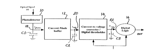
Figure 1 is a block schematic diagram of a first embodiment of the invention in
the form of an optical receiver comprising with a current-mode buffer and a current-to-
voltage conveyor;
Figure 2 is a schematic diagram showing in more detail the current-mode buffer
of the optical receiver of Figure l;
Figure 3 is a block schematic diagram of a second embodiment of the invention
which comprises a sense amplifier constituting a current-mode buffer and current-to-
voltage convertor;
CA 02204829 1997-0~-08
Figure 4 is a schematic diagram of the sense amplifier of the optical receiver of
Figure 3;
Figure 5 is a schematic diagram of a third embodiment of the invention
comprising a modified sense amplifier; and
Figure 6 shows the relationship between response time and input c~r~cit~nce for
current-mode receivers of the present invention and a voltage-mode receiver such as a
transimpecdance amplifier (TIA.).
DESCRIPTION OF THE PREFERRED EMBODIMENTS
Referring to Figure 1, an optical receiver comprises a photodetector unit 10,
current-mode buffer 12, current-to-voltage converter and thresholding circuit 14 and
digital processing circuit or logic 16. Circuits 14 and 16 are operable by a common
clock signal CLK.
A c~Iacitor Cl, shown in broken lines, lcprcsent~ the c~p~cit~nce at a node 18
15 bclween the photocletector unit 10 and the current-mode buffer 12, i.e. the capacitance
of the photodetector unit 10 and the input c~pacit~nce of the buffer 12. The value of Cl
is relatively high (e.g. 100's of femtoFarad - 1 picofarad) as compared with either the
capacitance C2 at the node 20 between current-mode buffer 12 and current-to-voltage
converter 14 or the capacitance C3 at the node 22 between converter/threshold circuit
20 14 and digital logic circuit 16, which might be 5-10 femtoFarads. C~r~cit~nces C2 and
C3 also are lcprcsenlcd by capacitors shown in broken lines.
The photodetector unit 10 converts the optical input signal into a correspondingphotodetector current Ipho~o~ which it supplies to the low-impedance input of current-mode
buffer 12. The buffer 12, which has a very low output capacitance, say 10 fF, supplies
25 a corresponding output current Io~t to the current-to-voltage converter/digital thresholder
14, which converts it into a collcs~onding output signal in the form of a digital voltage
which it applies to digital logic circuit 16 for further processing. The current-to-voltage
converter may be a low-, high- or transimpedance amplifier and the digital thresholder
may be a series of a~ru~?liately-sized inverters.
Figure 2 shows the photodetector unit 10 and current-mode buffer 12 in more
detail. The photodetector unit 10 is represented by two photodiodes 24 and 26 (e.g. PIN
diodes) connected in series between supply rails 28 and 30 which apply detector bias
voltages Vdet and -Vdet to the cathode of diode 24 and anode of diode 26, respectively.
CA 02204829 1997-0~-08
The node 18 between the two photodiodes 24 and 26 is connected to current-mode buffer
12. When a pair of differentially encoded optical beams (i.e. one bright (1) when the
other is dim (0)) are incident upon the photodiodes 24 and 26, respectively, each
generates a corresponding photocurrent which is a component of a bipolar input current
5 Iphoto which flows into or out of the node 18.
The current-mode buffer 12 comprises a push-pull current conveyor formed by
two "stacked" CMOS current mirrors 32 and 34 and an output stage 36. The currentmirror 32 is formed by two p-channel MOS field effect transistors 38 and 40 and two
N-channel MOSFETs 42 and 44. Each of the PMOSFET 38 and the NMOSFET 44 has
10 its drain and gate connected together. The gates of PMOSFETs 38 and 40 are connected
together and to the drain of FET 42. Likewise, the gates of NMOSFETs 42 and 44 are
connected together and to the drain of FET 40. The second current mirror 34 is of
similar construction, comprising MOSFETs 46, 48, 50 and 52, int~comlected in a
similar, complementary manner.
The two current mirrors 32 and 34 are "stacked," i.e. the sources of MOSFETs
42 and 50 are connected together at node 18 and the sources of MOSFETs 44 and 48 are
connected together; the sources of MOSFETs 38 and 40 are connected to a supply rail
at voltage Vdd, while the sources of MOSFETs 46 and 52 are grounded. The sources of
MOSFETs 44 and 48 are biased at Vdd/2. The detailed operation of the current mirrors
20 themselves will not be described here, since such circuits have been disclosed in
Electronics Letters, 12th. April 1990, Vol. 26, No. 8, for example. For further
information about current conveyors and their operation, the reader is directed to such
article and to United States Patent number 3,582,689 (issued June 1971), naming as
inventors K.C. Sedra and A. Sedra, and an article by B. Wilson entitled "Using Current
25 Conveyors," Electronics and Wireless World (April 1986).
The output stage 36 comprises two more MOSFETs 54 and 56. The source of
MOSFET 54 is connected to the supply rail Vdd and that of MOSFET 56 is grounded.The drains of MOSFET 54 and MOSFET 56 are connected together to the output (node20). The gate of output MOSFET 54 is connected to the gates of MOSFETs 38 and 4030 in current mirror 32 and the gate of output MOSFET 56 is connected to the gates of
MOSFETs 46 and 52 in current mirror 34.
In operation of the current conveyor, the currents are ~ rol~;d from channel to
channel. Thus, the components Ipl and Ip2 of input current Iphoto, which are input to
CA 02204829 1997-0~-08
current mirror 32 and current mirror 34, respectively, are "mirrored" or replicated as
currents Ipl' and Ip2' in the channels of MOSFETs 40 and 44 of current mirror 32 and
MOSFETs 48 and 52 of current mirror 34, respectively. The corresponding currents klpl'
and kIp2' at the drains of output MOSFETs 54 and 56, respectively, are proportional to
S Ipl and Ip2, respectively, but differ in amptitude according to the gain of the output stage
36. Such gain is detPrmined by the ratio between the channel width of MOSFET 54 and
MOSFET 38, and the ratio between the channel width of MOSFET 56 and MOSFET 46.
This gain improves the overall sensitivity of the receiver by providing more gain to the
input optical signal. The difference between the output current components klpl' and
10 kIp2' is the output current Io"t, which is outputted via node 20 and replicates the bipolar
input current Iphoto
Reca~lse FETs 42, 44, 48 and 50 are matched, a virtual short exists between the
input node 18 and the sources of FETs 44 and 48. Consequently, the input impedance
of the current-mode buffer 12 is very low, since the voltage swings at the high-
15 c~p~cit~nce input node 18 are reduced. The very low input impedance makes theor,llance less dependent upon input capacitance.
A second, more compact embodiment of the invention will now be described with
reference to Figure 3 in which, as before, a differential optical input is provided by a
photodetector unit comprising a pair of photodetectors 24 and 26. In this embo(liment7
20 however, the photodetectors 24 and 26 are connected to a compact current-mode sense
amplifier 60 which replaces the current conveyor unit 12 and current-to-voltage converter
14 of the embodiment of Figures 1 and 2. The sense amplifier 60 comprises a current
amplifier with a very low input impedance, and operates as a differential compal~or to
provide a digital output voltage dependent upon the "sense" of the input current. This
25 embodiment differs from the current conveyor embodiment of Figure 2, in that the input
is not only differential optically but also differential
electrically, i.e. each of the two photodetectors 24 and 26 is connected to its own node,
18' or 18".
As shown in Figure 4, the sense amplifier 60 comprises two p-channel MOS field
30 effect transistors 62 and 64 and two n-channel MOS field effect transistors 66 and 68
connected to form cross-coupled inverters. Thus, the drains of NMOSFETs 62 and 66
are connected together and their sources connected to the supply rail Vdd and tophotodetector 24, respectively. Likewise, the drains of MOSFETs 64 and 68 are
CA 02204829 1997-0~-08
connected together and their sources are connected to the supply rail Vdd and
photodetector 26, respectively. The gates of NMOSFETs 62 and 66 and the drains of
MOSFETs 64 and 68 are connected together. In a similar manner, the gates of
MOSFETs 64 and 68 and the drains of FETs 62 and 66 are connected together. The
5 digital output voltages VOUt and its complement V'OUt at the drains of MOSFETs 62 and
66 and the drains of MOSFETs 64 and 68, respectively, are supplied to output nodes 22'
and 22", respectively.
Two additional NMOSFETs 70 and 72 have their source electrodes connected
together to a source of a reference voltage V~ef and their gates connected to the supply
10 rail Vdd. Their drains are connected to the photodetectors 24 and 26, respectively. The
value of voltage V,efiS such that these MOSFETs 70 and 72 are biased into their linear
o~l~ting regions and help to keep the input potentials Vl' and V2' at the input to the
sense amplifier 60 close to each other, thus creating a "virtual short" at the inputs, i.e.
between PIN diodes 24 and 26.
A further NMOSFET 74 has its source and drain connected to the gates of
NMOSFETs 66 and 68, respectively, and its gate connected to a source of a clock signal
CLK. Another NMOSFET 76 has it source and drain connected to the sources of
NMOSFETs 66 and 68, respectively, and thus to the photodetectors 24 and 26,
respectively. Its gate is connected to the same source of clock signal CLK.
In operation, NMOSFETs 74 and 76 short-circuit the output and input,
respectively, in dependence upon the clock signal CLK. Thus, when the clock signal
CLK is high, the input and output are shorted and the sense amplifier is in a metastable
state wherein the output "floats". As soon as the clock signal CLK goes low, the short-
circuit is removed, the sense amplifier 60 becomes highly sensitive to the input data;
25 the output switches between digital levels in response to very small differences in optical
power at the differential input. Hence, the sense amplifier inherently performs both
current-to-voltage conversion and thresholding.
Figure 5 shows a third embodiment of the invention which comprises a
modification of the sense amplifier of Figure 4. The sense amplifier 60A of Figure 5
30 differs from that of Figure 4 in two ways. Firstly, two additional PMOSFETS 78 and
80, clocked by the clock signal CLK, are interposed between NMOSFETs 62 and 64 and
the supply rail Vdd. Thus, the drains of PMOSFETS 78 and 80 are connected to thesources of PMOSFETS 62 and 64, respectively, while the sources of additional
CA 02204829 1997-0~-08
PMOSFETS 78 and 80 are connected to the supply rail Vdd. Secondly, the NMOSFET
74 which, in Figure 4, short-circuits the output, is replaced by two NMOSFETs 82 and
84 which are both clocked by the clock signal CLK. NMOSFET 82 has its drain
connected to the drains of NMOSFET 66 and PMOSFET 62 and its source grounded.
5 Likewise, NMOSFET 84 has its drain connected to the drains of NMOSFET 68 and
PMOSFET 64 and its source grounded. Thus, the NMOSFETs 82 and 84 periodically
ground the outputs in dependence upon the state of the clock signal CLK. MOSFETs 78
and 80 charge the output nodes during the metastable states and disconnect the receiver
from supply rail Vdd during the "evaluate" period. The evaluate period is the time during
10 which the output signal is valid. When clock signal CLK is high, MOSFETs 78 and 80
are "closed" and the receiver is in a metastable state in which the output "floats" at a
level between zero and Vdd. When clock signal CLK goes low, MOSFETs 78 and 80
are "open" and the receiver is in the "evaluate" condition in which it is very sensitive
to input current changes. Very small input changes will cause the output to switch to
15 zero or Vdd.
This third modified embodiment is less susceptible to noise (right after the
metastable state) and is less prone to latching error. Moreover, this receiver can be
operated with a truly single phase clock and can be used in conjunction with dynamic
logic, hence providing low power in-situ proces~ing of received data.
Figure 6 illustrates, by way of example, the relationship between response time
and input c~p~it~nce for optical receivers of the present invention as compared with an
optical receiver which does not use a current-mode buffer. In Figure 6, the response of
the current-mode receiver (CM) is shown to be substantially independent of inputcapacitance. This is not the case for the transimpedance amplifier (TIA).
An advantage of embo-liment~ of the present invention is that, because the
current-mode buffer 12 has a very low input impedance, its speed is subst~nti~lly
independent of the input c~p~it~nce, which includes the capacitance of the
photodetectors. Consequently, the photodetectors may each have a relatively large light-
absorbing area, which facilitates optical ~lignmPnt of tr~n~ le~ ~ and receivers when the
30 optical receiver is used in optical interconnects. Another advantage is that they permit
greater freedom in the placement of the photodetectors on the chip plane.
Any of the embodiments disclosed herein can be interfaced directly with dynamic
or static digital logic circuitry for further processing.
CA 02204829 1997-0~-08
It should be appreciated that, although the prefelred embodiments disclosed herein
use either a current conveyor with an analog amplifier (current-to-voltage converter) or
a sense amplifier, the invention is not limited to these implementations. Rather, it is
envisaged that ~ltern~tive current-mode circuits might be employed to provide a low
5 i~ ?edallce interface to the photodetectors so as to reduce the effect of photodetector
c~r~cit~nce upon the output signal. Similar topologies (of current conveyors or sense
amplifiers) can be implemented using metal semiconductor field-effect translators
(MESFETs) or bipolar junction Tr~n.~mitters (BJTs). Moreover, the current conveyor
or sense amplifier could be implemented with different topologies.
Although embodiments of the invention have been described and illustrated in
detail, it is to be clearly understood that the same are by way of illustration and example
only and not to be taken by way of the limitation, the spirit and scope of the present
invention being limited only by the appended claims.