Note: Descriptions are shown in the official language in which they were submitted.
CA 02204931 1997-OS-09
.i
6'--
"MULTIPLE CHANNEL, MULTIPLE SCENE DIMMING SYSTEM"
This invention relates generally to lighting
controllers, and in particular to light dimming systems.
Light dimming systems are used to control
multiple lighting circuits which may be widely separated
from each other by a substantial distance, for example in
a restaurant, a large meeting hall or in a theater. The
lighting circuits are connected to power dimmers so that
the intensity of the lights can be controlled collectively,
individually or in groups whereby a variety of different
combinations of lighting levels may be selected for
achieving different lighting effects (scenes).
Typically, each light or group of lights is
selectively controlled through a power dimmer, which is in
turn connected to an individual controller or operator
switch. In such a system, separate sets of wires run from
a central controller to each light or group of lights.
Sometimes, dimmers are included along with wall-mounted
toggle switches for controlling the level of power supplied
to the separate lighting circuits: Such dimmers usually
take the form of rheostats which are manually set to the
desired level of brightness. Consequently, even for small
installations, a large amount of wiring is necessary to
connect all of the lights to their respective power
dimmers, and to connect the power dimmers to their respec-
tive controllers.
Conventional lighting control and dimming systems
provide a main switch control station and one or more
CA 02204931 1997-OS-09
t
-2-
remote dimming stations that are capable of independent
ON/OFF operation and dimming control. Such systems utilize
three-way and four-way dimmer switches in combination with
one or more traveler wires to provide independent ON/OFF
dimming operation at each remote location.
In a typical installation in which a single
overhead light is controlled and dimmed from a main station
and a remote station, a manual, two-way dimmer switch is
installed in a wall box at the main switch station, and a
manual, two-way dimmer switch is installed in a wall box at
the remote switch station. One side of the lamp load is
connected to the power source neutral conductor and the
other side of the lamp load is connected by a load conduc-
for to the main station switch. A hot conductor connects
the hot supply line to the remote dimmer switch. The main
dimmer switch and remote dimmer switch are further
interconnected by an auxiliary power distribution conduc-
tor, commonly referred to as a traveler conductor, a hot
line conductor and a ground safety conductor. In this two-
way switching and dimming arrangement, the lamp load is
wired in the conventional "switched hot" configuration.
Some remote dimmer switches have been connected
to a master dimmer controller in such installations, but
have required two or more additional wiring conductors and
a remote power supply for providing logic high and logic
low control signals to the master switch control circuit
for ON and OFF operation of the lighting load. In a
retrofit installation in which the main power switch and
CA 02204931 1997-OS-09
-3-
remote switch are to be replaced, it is desirable to remove
the switches at each switch station and install a main
dimmer controller in the main station wall box and a remote
dimmer in each remote station wall box. Moreover, it is
desirable to connect the remote dimmer switches to the main
dimmer switch control circuit by utilizing only the
existing traveler conductor and ground safety conductor
that interconnect the main and remote wall box switch
stations. In new wiring installations, a single conductor
(e. g. traveler conductor) interconnection of remote dimmer
stations with the master dimming controller is also
desirable for the purpose of simplifying the wiring
interconnections and for reducing wiring installation
costs.
In domestic and commercial installations, two-
phase power is supplied, with phase A power being applied
to one group of electrical loads, and phase B power being
applied to another load group. Consequently, in a large
area lighting installation, some of the lighting loads will
be supplied by phase A power, and other lighting loads will
be supplied by phase B power. Dimming systems typically
utilize semiconductor switching devices whose duty cycle is
controlled with reference to the phase of the current
waveform. Because of the phase difference, it is difficult
to utilize conventional light dimming systems which employ
a microprocessor controlled memory unit for selectively
controlling the application of power to a specific group of
CA 02204931 1997-OS-09
-4-
lighting loads, individual ones of which may be separately
energized by phase A and phase B power.
Consequently, a light dimming system is needed in
which the amount of wiring required for connecting a
controller to multiple power dimmers is substantially
reduced. Such a lighting control and dimming system
desirably should be operable via a single conductor by
which several individually-dimmable lighting loads can be
controlled without appreciably increasing the amount of
wiring. Moreover, in large area lighting, multiple power
phase installations, the lighting control and dimming
system should be capable of reliable operation in which
dimmer station address signals from a remote controller or
a master controller can be communicated independently of
line phase per dimmer station or controller station.
According to one aspect of the present invention,
a lighting control and dimming system utilizes a single
conductor, for example the traveler conductor of existing
wiring, for transmitting analog data signals to each dimmer
of a light/dimmer group. The master controller includes a
signal generator for generating a unique and predetermined
analog data signal corresponding to a predetermined
lighting intensity level for a particular scene. The
predetermined analog data signals are stored in a read-only
memory of a microcontroller in the master controller and
are transmitted serially over the traveler conductor to
each dimmer unit. Each dimmer unit includes a micro
CA 02204931 1997-OS-09
-5-
controller and read-only memory in which corresponding
dimmer unit identification binary numbers are stored.
In response to operator selection of a predeter-
mined scene, the microcontroller selects from memory the
corresponding binary data signal and transmits it serially
as an analog data signal over the traveler conductor to an
input shift register in each dimmer. The data content of
the input shift register is compared, bit-by-bit, with a
binary number stored in the dimmer ROM. A serial bit
comparator produces an enable signal in response to a bit-
by-bit identity match between the transmitted analog data
signal and the preset binary identification number stored
in the dimmer ROM. Only a match between the transmitted
analog data signal and the stored binary number will
produce a predetermined scene. After being enabled, the
dimmer can be manually adjusted to a new intensity setting,
as desired.
According to another aspect of the invention, the
remote signalling and selection of a specific scene is made
independently of phase by sampling the logic value of the
remote input analog data signal immediately following a
logic 1 to logic 0 transition of a zero cross signal. If
the high to low transition occurs at any time during which
the zero crossing signal is low, logic 1 is loaded into
each dimmer remote input shift register. If no high-to-low
transition occurs during that period, that particular bit
of the remote input shift register is cleared to logic 0.
Each time the zero crossing signal returns to logic high,
CA 02204931 1997-OS-09
-6-
the contents of each dimmer remote input register are
shifted and the contents of each input register are
compared bit-by-bit to the contents of the binary unit
identification number that is stored in the read-only
memory of each dimmer microcontroller. A particular dimmer
is enabled in response to a match between the analog remote
signal and the preset binary number.
Operational features and advantages of the
present invention will be further understood upon consider
ation of the following detailed description of the inven
tion taken with reference to the accompanying drawings, in
which:
FIGURE 1 is a block schematic diagram of a multi-
channel, multiple scene lighting and dimming circuit
constructed according to the present invention;
FIGURE 2 is a block schematic diagram of the
master controller shown in FIGURE 1;
FIGURE 3 is a simplified circuit diagram of the
serial bit comparator of FIGURE 2;
FIGURE 4 is a simplied schematic block diagram of
an edge detector circuit for practicing the methods
illustrated by the waveforms of FIGURES 5, 6, and 7;
FIGURE 5 is a waveform diagram of the analog data
signal corresponding with a HEX-A pulse train;
FIGURE 6 is a waveform diagram of the zero cross
signal appearing on the output of the zero cross detector;
CA 02204931 1999-06-18
_7_
FIGURE 7 and FIGURE 8 are waveform diagrams
corresponding with FIGURE 5 and FIGURE 6, which illustrate
an alternative high-to-low transition detection method;
FIGURE 9 is a block schematic diagram of a
lighting and dimming circuit which includes local and
network remote controllers; and,
FIGURE 10 is a schematic diagram of the low pass
attenuator circuit shown in FIGURE 9.
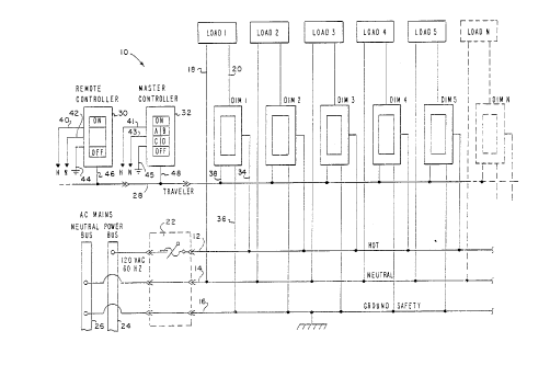
Referring now to FIGURE 1, the lighting control
system 10 of the present invention will be described with
reference to the hot, neutral and ground safety power
conductors 12, 14 and 16, respectively, of a 120 VAC, 60 Hz
single phase AC power source which supplies operating power
to multiple lighting loads LOAD 1, LOAD 2, . . . , LOAD N.
According to conventional AC wiring practice, one terminal
of a lighting load, for example LOAD 1, is connected to the
neutral supply conductor 14 by a load conductor 18 , and the
other terminal of LOAD 1 is connected to the switched
terminal of a dimmer switch DIM 1 by a load conductor 20.
Preferably, the dimmer switch DIM 1, in part, is a program-
enable dimmer as described and claimed in U.S. Patent
4,733,138 and U.S. Patent 5,194,858.
Operating power is conducted through a thermal
circuit~breaker 22 which connects the conductor 12 and an
AC power bus 24. Load current is returned through the
neutral conductor 14 to a neutral bus 26. According to
CA 02204931 1997-OS-09
_g_
conventional practice, the ground safety conductor 16 is
also electrically connected to the AC neutral bus and is
routed in parallel with the hot conductor 12 along the
distribution path for safety purposes. At least the hot
conductor 12 and the ground safety conductor 16 is avail-
able at each dimmer station. A traveler conductor 28 is
also available in addition to the hot and ground safety
conductors between the dimming stations.
In a typical system, the lighting control system
of 10 includes a remote controller 30 and a master control-
ler 32. The number of dimmer switches which may be coupled
to the master controller 21 is limited to approximately 24
channels because of fan-out loading, since the dimmers draw
operating current in the standby operating mode.
Referring now to FIGURE 1 and FIGURE 2, the
dimmer switches DIM 1, DIM 2, ..., DIM N have identical
circuit construction. The dimmer switch DIM 1 has a first
power input conductor 34 connected to the hot power
conductor 12 and a second power input conductor 36 con-
nected to the ground safety conductor 16. The dimmer
switch DIM 1 also includes a signal input conductor 38
which is electrically connected to the traveler conductor
28 which leads from the remote controller 30 and master
controller 32 to each dimmer unit.
The remote controller 30 includes input power
conductors 40, 42, 44 electrically connected to the hot,
neutral and ground conductors 12, 14, 16, respectively, and
a signal output conductor 46 which is electrically con-
CA 02204931 1997-OS-09
_g_
nected to the traveler conductor 28. The traveler conduc-
for 28 is electrically connected to a remote signal output
node 48 of the master controller unit 32. The master
controller 32 includes input power conductors 41, 43 and 45
electrically connected to the hot, neutral and ground
safety conductors 12, 14 and 16, respectively.
It will be appreciated that the dimmer switch
stations DIM 1, DIM 2, DIM 3, ..., DIM N of a typical
installation are widely separated with respect to each
other, and with respect to the remote controller 30 and the
master controller 32. Thus, at each dimming station and
each controller, at least the hot conductor 12, the ground
safety conductor 16 and the traveler conductor 28 are
available for interconnection, but only the traveler
conductor is required to be a common physical conductor
connected to each unit for sending and receiving control
signals independently of the line phase of power supplying
each dimmer or controller.
Consequently, the dimmers, master controller and
remote controller are wire-for-wire interchangeable with
conventional two-way manual power switches. Each dimmer
switch, the master controller and remote controller include
manually operable, momentary contact switches designated ON
and OFF, respectively. According to this arrangement,
independent ON/OFF manual switch operation is provided at
each controller and dimmer station.
Referring now to FIGURE 2, a master controller 32
is shown that is capable of storing four scenes correspond-
CA 02204931 1997-OS-09
-10-
ing with four separate intensity levels (A, B, C, D), in
addition to ON and OFF connections and is connected in
communication with one of the dimmer units DIM 1 via the
traveler conductor 28 in the same manner as each of the
other dimmer units of the system are connected. The
controller includes a microcontroller 50, a read-only
memory 52, a power supply 54 and a serial encoder register
56. These components are arranged in the form of an
information storage and retrieval system for storing a
predetermined number of scenes and performing all the
necessary control functions.
The microcontroller 50 may be any one of several
conventional microcontrollers that are commercially
available. The type of microcontroller used is largely
dependent upon the capacity desired, and is designed so
that a variety of logical and arithmetic operations may be
performed on or between two accumulation registers includ-
ing additions, subtractions, logical ANDS, OR'S, compares,
complements, tests and shifts. Dedicated registers (not
shown) are used for control of the system, and include a
program counter, an index register, a stack pointer and a
condition code register. These are generally controlled by
the microcontroller logic, although they may be used or
altered under the control of a stored operating program.
The microcontroller 50 includes a read-only
memory (ROM) 52 in which an operating program is stored.
The operating program allows user programs and data to be
stored in the read-only memory, the working registers to be
CA 02204931 1997-OS-09
-11-
examined and the execution of the user program to be
supervised. Preferably, the read-only memory 52 is
implemented by an electrically programmable read-only
memory (EPROM).
The master controller 32 includes an ON switch,
an OFF switch and four pre-set scene switches labeled A, B,
C and D. All of these switches are single pole, single
throw, non-latching push-button switches. The depression
of each switch provides a connection to a ground reference
l0 voltage from a local power supply 54 and supplies the
microcontroller 50 with a logical "zero" input. The
microcontroller 50 recognizes the logical zero as a signal
that the switch has been depressed. Other configurations
of the switches are possible, provided that each switch
have an operative and a non-operative position in order to
provide logic signals to the microcontroller. The ON
switch provides a fade "up" function when it is depressed
and held. Likewise, the OFF switch provides a fade "down"
switch which is operative when it is depressed and held in
the closed position. The switches A, B, C and D correspond
with four predetermined hexadecimal numbers, HEX-A, HEX-B,
HEX-C and HEX-D which are stored in the read-only memory
52.
The operating program of the microcontroller 50
addresses the various input switches and determines the
status of each switch. When a preset switch is depressed,
its status is logic low and the operating program of the
microcontroller issues a command that retrieves the
CA 02204931 1997-OS-09
-12-
corresponding HEX-coded signal from the read-only memory
and inputs the HEX-coded signal to the serial encoder
register 56 . In the example shown in FIGURE 2 , preset
switch A is depressed, with HEX signal HEX-A being re-
trieved and input into the serial encoder register 56. The
analog data signal corresponding with HEX-A is transmitted
to the traveler conductor 28 through an output conductor
48.
In the output mode, a communications interface
transfers the coded signal HEX-A over an internal bus to
the serial encoder register 56 according to a clock signal
55. Condition codes determine the transmission rate and
the number of start, stop and parity bits required. In the
example given herein of HEX-coded signals, all bits are
information bits. The number of start, stop and parity
bits is zero. The complete analog data word HEX-A is
shifted out of the serial encoder register 56 through the
output conductor 48 at the predetermined clock rate.
FIGURE 5 shows the form of the analog data signal which is
a series of pulses of variable duration between a high
value (+V) representing logic "1" and a low value (-V)
representing logic "0".
Each dimming unit, such as DIM 1, includes a
decoder 58 for receiving, decoding and comparing the remote
analog signal HEX-A and comparing it with a predetermined
HEX coded unit identification number in a read-only memory
60. The encoded analog signal HEX-A is input from the
CA 02204931 1997-OS-09
-13-
traveler conductor 28 through an input conductor 62 to a
shift register 64.
Referring to FIGURE 2, the controller 32 and
dimmer DIM 1 could be respectively powered by different
phases of a two-phase AC power distribution system. In
such a multiple phase system, the remote signalling and
selection of each dimmer having a binary number stored in
the EPROM memory 60 is made independently of the applied AC
power phase by sampling the logic value of the remote input
signal in relation to a zero cross signal of the AC line
voltage applied to the dimmer. For this purpose, a zero
cross detector 66 produces a zero cross signal 68 that is
derived from zero cross transitions of the line voltage on
the hot conductor 12.
In accordance with one technique generally
illustrated in FIGURES 5 AND 6, if a high-to-low transition
of the remote input signal occurs at any time during which
the zero crossing signal is low, the least significant bit
of the dimmer input register 64 is set to logic "1". Such
transitions are shown by the arrows on the waveforms of
FIGURE 5. If no high-to-low transition occurs during that
period, that particular bit of the dimmer input register is
cleared to logic "0". Each time the zero crossing signal
returns to logic high, the contents of each dimmer register
are shifted.
After shifting, the contents of each input
register dimmer are compared bit-by-bit to HEX-coded
numbers which are stored in the read-only memory 60 of the
CA 02204931 1997-OS-09
-14-
dimmer microcontroller 78. Each dimmer is enabled in
response to a bit-by-bit match between the analog remote
signal and a HEX-coded number stored in the memory of that
dimmer. As shown in FIGURE 2, DIM 1 includes a semiconduc-
for switching device, such as a thyristor having a gate "g"
that is responsive to an enable signal from comparator 72.
Referring now to FIGURE 4, FIGURE 5 and FIGURE 6,
in response to a high-to-low transition of the zero cross
signal 68, the operating program of the microcontroller 78
retrieves a binary number (for example, HEX-A) stored in
the read-only memory 60 and inputs it to a serial encoder
register 70. Each time the zero crossing signal returns to
logic high, the contents of the dimmer shift register 64
and the serial encoder register 70 are shifted by the
output of an edge detector circuit 99, which is a portion
of the decoder 58, as shown in FIGURE 4. The bit contents
of each register are conducted to a serial bit comparator
72 through output buses 74, 76, respectively. FIGURES 5
and 6 have similar horizontal time axes.
Referring now to FIGURE 3, the shift register 64
and the serial encoder register 70 are six bit shift
registers that are designed to hold the bits of the HEX
encoded data word transmitted over the traveler conductor
28. In the present example, where the HEX encoded data
word contains six bits of information, the encoded analog
signal on conductor 62 is fed one bit at a time into the
shift register 64 until all six bits are contained in the
register and are simultaneously conducted over the corre-
CA 02204931 1997-OS-09
-15-
sponding six output lines 64A, 64B, 64C, 64D, 64E and 64F.
Likewise, the binary number HEX-A, which was previously
stored in the read-only memory 60, is retrieved by a
microcontroller 78 and is fed one bit at a time into the
serial encoder register 70 until all six bits are contained
in the register. The logic value of each bit stored in the
serial encoder register 70 is conducted over output lines
70A, 70B, 70C, 70D, 70E and 70F.
Corresponding bits 64F and 70F are simultaneously
applied to the inputs of an exclusive OR (XOR) gate 80 for
comparison. Likewise, the corresponding bit pairs of the
remaining bits of each register are input to exclusive OR
(XOR) gates 82, 84, 86, 88 and 90, respectively, for
comparison of each bit pair. According to the logic of an
exclusive OR (XOR) gate, a logic zero on both inputs yields
a logic zero and a logic one on both inputs yields a logic
zero. If there is a logic match between corresponding
bits, the output of the exclusive OR gate will be logic
zero. Consequently, when there is an identical match
between the remote analog data word (HEX-A) and the binary
number (HEX-A) stored in the read-only memory 60, the
output of each XOR gate is logic zero.
The outputs of the XOR gates are inverted by
inverters 92, 94, 96, 98, 100 and 102, respectively. The
inverted outputs are input to an AND gate 104 which
provides a logic one enable signal 106 when each of its
inputs is at logic one value. This will occur only when
there is an exact match between the encoded remote signal
CA 02204931 1999-06-18
-16-
(HEX-A) and the binary numbers stored in the read-only
memory 60 (HEX-A). Under this condition, the output of
each XOR gate is logic zero, and each inverted output is
logic one. In response to that condition, the AND gate 104
produces a logic one signal on the output conductor 106,
and is logic zero under all other input conditions.
The ON function and the OFF function are gener-
ated in response to all data bits of the shift register 64
being at logic one value (ON function), or all data bits
are logic zero (OFF function) . The output of each data bit
is input to an AND gate 108 which produces the ON signal in
response to each input being at logic one value. Likewise,
the bit contents are input to a NOR gate 10 Q . According to
the logic function of a NOR gate, a logic high output is
produced in response to each input being at logic zero
value. By this arrangement, the OFF signal is produced
when each bit of the shift register 64 is at logic zero.
Accordingly, it will be seen that each dimmer
unit can be loaded with unique encoded numbers which
correspond to the encoded unit identification numbers
stored in the read-only memory 52 of a remote controller or
the main controller 32 in order to obtain a particular
dimming level on the dimmer output. When an input switch
(ON, A, B, C, D, OFF) is depressed, encoded analog signals
are conducted over the traveler conductor 28 as a serial
stream of analog pulses that are applied to the shift
register 64 input of each dimmer unit. In this manner,
each dimmer unit is enabled by manually depressing one of
CA 02204931 1997-OS-09
-17-
the selector switches that results in the above-described
match occurring.
The master controller 32 of FIGURES 1 and 2
allows selection of any scene, fade to "FULL" (ON) or "OFF"
and raise or lower all dimmers together, without losing the
scene or preset memories. The remote controller of FIGURE
1 has selector switches that will select only the ON scene
or the OFF scene and raise or lower all channels together.
For selection of a specific scene, the desired switch ON,
A, B, C, D or OFF is depressed in the master controller.
The current scene switch includes a light emitting diode
(LED) , not shown, which will glow to indicate scene status.
To raise all dimmer channels together, the ON scene switch
is pressed and held until the lights reach the desired
intensity. When all channels are raised or lowered
together, the system is in the ON condition, although each
dimmer is not necessarily at its preset ON level and may,
in fact, be at a lower intensity.
Referring now to FIGURE 7 and FIGURE 8, in an
alternative embodiment of a signal decoding technique, the
microcontroller 78 of each dimmer includes another subrou-
tine program that performs exactly as stated above except
that it waits for the zero crossing to transition high
before checking the remote input 62 of the decoder 58.
This is necessary to accommodate a condition in which the
first routine is not able to decode the remote pulse train
correctly, thereby assuring more reliable operation.
CA 02204931 1997-OS-09
-18-
According to an alternative method of decoding
the four remote signals (A, B, C, D), each time a zero
crossing signal makes a high to low transition, such as
shown by the down directed arrows in FIGURE 8, the remote
input to the microcontroller is sampled to obtain the logic
level. If the remote input is high, then the least
significant bit (LSB) of a first remote input register is
set to logic "1". If the remote input is low when the zero
crossing makes its high to low transition, then the LSB of
the register is cleared to logic zero ( "O" ) . After setting
or clearing this bit, the register contents are shifted
left and an exclusive OR operation is performed between the
first remote input register, and a second remote input
register. The result of the exclusive OR (XOR) operation
is then compared with the four binary numbers for the four
dimmer scenes. If there is a match, then the dimmer has
successfully decoded a remote signal.
In the second remote memory register, the status
of the remote input for the microcontroller 78 is stored
based in response to a low to high transition of the zero
crossing signal. For example, when the zero crossing
signal changes from a low logic level to a high logic
level, such as shown by the up directed arrows in FIGURE 8,
the remote input 62 to the micrcontroller is read to check
its logic level. If it is high, then the least significant
bit (LSB) of the second remote input register is set to
logic high ("1"). If it is logic low, then the LSB of the
remote input register No. 2 is cleared to a zero. After
CA 02204931 1999-06-18
-19-
setting or clearing this bit, the register contents are
shifted left.
Referring now to FIGURE 9 and FIGURE 10, a low
pass attenuator circuit 110 is interposed between the
remote master controllers 30, 32 and the dimmer DIM 1. The
attenuator circuit 110 permits a single remote controller,
for example remote controller 30, to change a single
dimming station, for example DIM 1, without affecting the
intensity setting of any of the other dimmers that are
connected to the network traveller conductor 28. Prefera-
bly, the attenuator circuit 110 provides attenuation in a
ratio of about 20:1. The attenuator circuit 110 includes
a low pass filter 112 connected in series with the local
remote controller 30 on input conductor 46 and input node
33 to decoder 58. In this example, the low pass filter 112
includes series resistors R20 and R21 with resistor R19 and
capacitor C10 connected to respective terminals of resistor
R20. R19 and C10 have other terminals that are grounded.
The network traveller 28 is decoupled with
respect to the input terminal node 33 of the dimmer DIM 1
by a circuit portion 114 which is connected in series
electrical circuit relation between traveler 38 and input
node 33. In circuit portion 114, a diac diode D3 presents
a high impedance to the flow of current from the input node
33 through the network remote controller input terminal
from conductor 38. Circuit portion 114 also has a low pass
filter comprising, in this example, series resistors R8 and
R4 with resistor R18, capacitor C6 and capacitor C9 each
CA 02204931 1997-OS-09
-20-
having a terminal connected respectively to a first
terminal of R8, a second terminal of R8, and the side of R4
connected to the input node 33. Second terminals of R18,
C6 and C9 are grounded.