Note: Descriptions are shown in the official language in which they were submitted.
CA 0220~0~8 1997-0~-09
~'
~ ~ b ~,
SPECIFICATION
Three-Dimension Image Processing Apparatus
FIELD OF ARTS
This invention relates to a three-dimension image processing apparatus and an
external memory device to be used therefor, and more particularly to a three-dimension
image processing apparatus which is adapted to display on a display an inlage of an
operable object or other objects, existing in a three-dimensional space, photographed
from a predetermined photographing position (the point of eye).
PRIOR ARTS
The conventional so-called 3D (~3-Dimensional) game has an operable obJeGt
(object operable by an operator) configured by three-dimensional data photographed by
a camera at predetermined angle and distance, thereby obtaining displaying images.
-In the conventional game, however, if there comes a background image or an
- object being used as an opponent character (another object) between the operable object
and the camera, or if another object is moved to interrupt between the operable object
and the camera, the operable object is rendered impossible to be photographed.
To this end, there has been a limitation in the conventional 3D game in that theother object has to be arranged by a program not to exist between the operable object and
the camera.
SUMMARY OF THE INVENTION
It is therefore the primary object of the present invention to provide an image
processing apparatus which is capable of displaying an operable object at all times and
CA 0220~0~8 1997-0~-09
hence free from limitation in arranging other objects.
The present invention lies in an image processing apparatus adapted to display on
a display an image photographed of an operable object and another object existing in a
three-dimensional space from a predetermined photographing position, comprising: an
external memory means which stores data of the operable object and the other object
and, a predetermined program; an input means which inputs data which alters the
position of the operable object in the three-dimensional space; an operable object
position data generating means which generates operable object position data so as to
alter the position of the operable object in the three-dimensional space based on the data
inputted by the input means; a three-dimensional data creating means which creates
three-dimensional data based on the data stored in the external memory means and the
operable object position data; a photographing position data generating means which
generates photographing position data representative of a photographing position in the
three-dimensional space for photographing the operable object; a detecting means which
detects whether or not the other object is existent between the photographing position
and the operable object position; a photographing position data altering means which
alters the photographing position data such that the other object is not existent between
the photographing position and the operable object position when the detecting means
detects existence of the other object; a display data creating means which creates display
data for displaying the image of the operable object photographed from a predetermined
position in the three-dimensional space based on the three-dimensional data and the
photographing position data; and an image signal generating means which outputs an
image signal to the display based on the display data created by the display data creating
means.
The detecting means determines whether or not there is a possibility of collision
CA 0220~0~8 1997-0~-09
--- between the operable object and a polygon plane of the other object. If there is a
possibility of colliding the operable object with the other object, the photographing
position data altering means alters the photographing position, i.e., the position of a
camera, so that the other object doe not exist between the operable object and the
5 camera. Therefore, the operable object is photographed without being interfered by the
other object.
In accordance with the present invention, even if another object is freely
arranged, it is possible to display at all times an operable object on a screen of a display.
Consequently, if the present invention is applied to a game apparatus, the operable
10 object can be displayed at all times on a display even for a game that involves an
operable object and a number of other objects moving around on the display screen.
The above and other objects, features, aspects, and advantage of the present
invention will become more apparent from the ensuing detailed description of the
present invention when taken in conjunction with the accompanying drawings.
BRIEF DESCRIPTION OF THE DRAWINGS
Figure 1 is a schematic illustrative view showing one embodiment of the present
invention;
Figure 2 is a block diagram showing in detail an image processing apparatus in
20 the Figure 1 embodiment;
Figure 3 is an illustrative view showing a memory map in CPU of the Figure 2
embodiment, demonstrating an external memory and a W-RAM incorporated in a
cartridge;
Figure 4 is a block diagram showing in detail a controller control circuit in the
25 Figure 2 embodiment;
CA 0220~0~8 1997-0~-09
-- ~ Figure 5 is an illustrative view showing a mo~ ting/demodulating method for
data;
Figure 6 is an illustrative view showing a memory map of a RAM in Figure 4;
Figure 7 is a perspective view of a controller of the Figure 2 embodiment as
5 viewed from the above;
Figure 8 is a perspective view of the controller of the Figure 2 embodiment as
viewed from the bottom;
Figure 9 is a block diagram showing in detail the controller and an expansion
device;
Figure 10 is an illustrative view showing data on an analog joystick of the
controller and respective buttons;
Figure 11 is an illustrative view of tr~n~mi.cc ion and reception data by the control
circuit when a command "0" is transmitted from the controller control circuit;
Figure 12 is an illustrative view of tr~n~mi~ion and reception data by the control
circuit-when a command "1" is transmitted from the controller control circuit;
Figure 13 is an illustrative view of tr~n.~mi.c.~ion and reception data by the control
circuit when a command "2" is transmitted from the controller control circuit;
Figure 14 is an illustrative view of tr~n~mi.c;c ion and reception data by the control
circuit when a command "3" is transmitted from the controller control circuit;
Figure 15 is a flowchart showing operation of the CPU of the Figure 2
embodiment; Figure 16 is a flowchart showing operation of the bus control circuit of the
Figure 2 embodiment;
Figure 17 is a flowchart showing operation of the controller control circuit of the
Figure 2 embodiment;
Figure 18 is a flowchart showing operation of the controller circuit of the Figure
CA 0220~0~8 1997-0~-09
-
- ~.,
---= Y 2 embodiment;
Figure 19 is an illustrative view of tr~nsmi~ion and reception data by the control
circuit when a command "255" is tr~n~mitted from the controller control circuit;Figure 20 is an illustrative view showing a state that a wall exists between theoperable object (Mario) and the camera;
Figure 21 is an illustrative view showing in coordinate the state of Figure 20;
Figure 22 is a flowchart showing operation for a camera turning-around process;
Figure 23 is a flowchart showing a collision-determining routine;
Figure 24 is an illustrative view showing a wall polygon;
Figure 25 is an illustrative view showing each polygon;
Figure 26 is an illustrative view showing a projected surface;
Figure 27 is an illustrative view showing a state that projection is onto a YZ
plane;
Figure 28 is an illustrative view showing a state that projection is onto an XY
plane;-and
Figure 29 is an illustrative view showing a normal vector of the plane and an eye
vector of the camera.
EMBODIMENTS
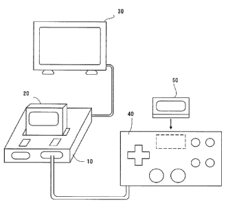
Referring to Figure 1, there is illustrated an external view showing a system
structure of an image processing system according to one embodiment of the present
invention. The image processing system is for example a video game system, whichinclusively comprises an image processing apparatus main body 10, a ROM cartridge 20
as one example of an external memory device, a display 30 as one example of a display
means connected to the image processing apparatus main bodylO, a controller 40 as one
CA 0220~0~8 1997-0~-09
-
--- ~ example of an operating means, and a RAM cartridge 50 as one example of an extension
device detachably attached to the controller 40. Incidentally, the external memory
device stores image data and program data for image processing for games, and audio
data for music, effect sound, etc. A CD-ROM or a magnetic disc may alternatively be
S employed in place of the ROM cartridge. Where the image processing system of this
example is applied to a personal computer, an input device such as a keyboard or a
mouse is used as the operating means.
Figure 2 is a block diagram of the image processing system of this example. The
image processing apparatus 10 incorporates therein a central processor unit (hereinafter
"CPU") 11 and a bus control circuit 12. The bus control circuit 12 is connected with a
cartridge connector 13 for detachably attaching the ROM cartridge 20, as well as a
working RAM 14. The bus control circuit 12 is connected with an audio signal
generating circuit 15 for ouLpul~ g an audio signal processed by the CPU 11 and a video
signal generating circuit 16 for outputting a video signal, and further with a controller
15 control circuit 17 for serially transferring operating data of one or a plurality of
controller(s) 40 and/or data of RAM cartridge(s) 50. The controller control circuit 17 is
connected with controller connectors (hereinafter abbreviated as "connectors") 181 -
184 which are to be provided at a front face of the image processing apparatus 10. To
the connector 18 is detachably connected a connection jack 41 and the controller 40
through a cable 42. Thus, the connection of the controller to the connector 181 - 184
places the controller 40 into electric connection to the image processing apparatus 10,
enabling tr:~n~mi~ion and reception of data therebetween.
More specifically, the bus control circuit 12 inputs therein a command outputted
by a parallel signal from the CPU 11via a bus to parallel-serial convert it for outputting a
command by a serial signal to the controller control circuit 17, and converts serial signal
CA 0220~0~8 1997-0~-09
-- ~ data inputted from the controller control circuit 17 into a parallel signal for oul~u~tillg it
to a bus. The data outputted through the bus is subjected to processing by the CPU 11,
stored in W-RAM 14, and so on. In other words, the W-RAM 14 is a memory temporary
storing the data to be processed by the CPU 11, wherein read-out and write-in of data is
5 possible through the bus control circuit 12.
Figure 3 is a diagrammatic illustration showing memory regions assigned to
respective memory spaces. The memory spaces accessible by the CPU via the bus
control circuit 12 involves an external memory region of the ROM cartridge 20 and a
memory region of the W-RAM 14. Although the ROM cartridge 20 is structured by
10 mounting on a board a ROM stored with data for game processing and accommodating
the same board in a housing, the ROM storage data is shown by the external memory
region shown in Figure 3. That is, the ROM includes an image data region 201 stored
with image data required to cause the image processing apparatus 10 to generate image
signals for the game, and a program data region 202 stored with program data required
for predetermined operation of the CPU 11. In the program data region 202, there
fixedly stored are an image display program for performing image display based on
image data 201, a time-measuring program for carrying out measurement of time, and a
determination program for determining that the cartridge 20 and an extension device 50,
hereinafter referred to, are in a predetermined relationship. Incidentally, the details of
20 the time-measuring program and the determination programs will be stated later. On the
other hand, the memory region of W-RAM 14 includes a region 141 for temporarily
storing data representative of an operating state from a control panel.
Figure 4 is a detailed circuit diagram of a controller control circuit 17. The
controller control circuit 17 is provided for tr~nsmi~ion and reception of data in serial
between the bus control circuit 12 and the controller connector 181 - 184, and includes a
CA 0220~0~8 1997-0~-09
-~ ~ data transfer control circuit 171, a signal tr~ns~mitting circuit 172, a signal receiving
circuit 173 and a RAM 174 for temporarily storing transmission and reception data. The
data transfer control circuit 171 includes a parallel-serial conversion circuit and a
serial-parallel conversion circuit for conversion of data format during data transfer,
5 which also performs control of write-in and read-out of the RAM 174. The serial-
parallel conversion circuit converts serial data supplied from the bus control circuit 12
into parallel data to provide it to the RAM 174 or the signal transmitting circuit 172. The
parallel-serial conversion circuit converts parallel data supplied from the RAM 174 or
the signal receiving circuit 17~ into serial data to provide it to the bus control circuit 12.
10 The signal transmission circuit 172 converts data for signal read-in control of the
controller 40 supplied from the data transfer control circuit 171 and write-in data
(parallel data) to the RAM cartridge S0 into serial data, which data is tr~n.~mitted through
a corresponding channel CHl - CH4 to each of the plurality of controllers 40. The signal
receiving circuit 173 receives in serial read-out data, representative of an operating state
15 of each of the controller 40, inputted through a corresponding channel CHl - CH4 to
each of the controller 40 as well as read-out data from the ~AM cartridge 50, to convert
them into parallel data to provide it to the data transfer control circuit 171.
The signal transmitting circuit 172 and the signal receiving circuit 173 adopt a
duty-cycle modulation and demodulation (hereinafter referred to as
20 "modulation/demodulation") method as one example of the modulation/demodulation
method. The duty-cycle modulation/demodulation method, as shown in Figure 5, is a
modulation/demodulation method wherein "1" and "0" are represented by varying a Hi
time period and a Lo time period for a signal at a certain interval. Explaining the
modulation/demodulation method with more detail, when data to be transmitted in serial
25 is a logical "1" a signal having, within one cycle period T, a high-level period tH
CA 0220~0~8 1997-0~-09
.,,
rendered longer than a low-level period tL (tH > tL) is transmitted, while when data to be
transmitted is a logical "0" a signal having, within one cycle period T, tH rendered
shorter than tL (tH < tL) is transmitted.
In the meanwhile, the demodulation method makes sampling on a serial signal
5 received (bit tr~n~mi~.~ion signal) so as to monitor at all times whether the received
signal is at a high level or a low level, wherein one cycle is expressed as T = tL + tH
provided that time period of low till change to high is tL and time period of high till
change to low is tH. In this case, the relation of tL and tH being tL < tH is recognized as
logical "1", while tL > tH is recognized as logical "0", thereby achieving demodulation.
10 If the duty-cycle modulation/demodulation method like this is employed, there is no
necessity of transmitting data in synchronism with clock, offering an advantage that
tr~n~mi.~.~ion and reception of data are available with only one signal line. Incidentally,
it is natural that if two signal lines are available another modulation/demodulation
method may be utilized.
The RAM 174 includes memory regions or memory areas 174a - 174h as shown
in a memory map of Figure 6. Specifically, the area 174a is stored with a command for
channel 1, while the area 174b is stored with tr~n~mi.~ion data and reception data for
channel 1. The area 174c is stored with a command for channel 2, while the area 174d is
stored with trzln.~mi.~ion data and reception data for channel 2. The area 174e is stored
with a command for channel 3, while the area 174f is stored with tr~n~mi.~.cion data and
reception data for channel 3. The area 174g is stored with a command for channel 4,
while the area 174h is stored with tr~n~mi.~ion data and reception data for channel 4.
Accordingly, the data transfer control circuit 171 operates to write-in control to
the RAM 174 data transferred from the bus control circuit 12 or data of operating state of
the controller 40 received by the signal receiving circuit 173 or read-out data from the
CA 0220~0~8 1997-0~-09
,
-
RAM cartridge 50, and read data out of the RAM 174 based on a command from the bus
control circuit 12 to transfer it to the bus control circuit 12.
Figure 7 and ~igure 8 are outside appearances at main and back surfaces of a
controller 40. The controller 40 is in a shape that can be grasped by both hands or one
hand, and has a housing having an exterior formed projecting with a plurality of buttons,
when depressed, for generating an electric signal and a vertically-standing control
portion. Specifically, the controller 40 is constituted by an upper housing and a lower
housing. The housing of the controller 40 has an operating area formed on an upper
surface in a planar shape long sideways. In the operating area of the controller 40, there
are provided a cross-shaped digital direction switch (hereinafter referred to as "cross
switch") 403 on a left side, a plurality of button switches (hereinafter merely
abbreviated as "switches") 404A - 404F on a right side, a start switch 405 generally at a
laterally central portion, and a joystick 45 for allowing analog inputting at a centrally
lower portion. The cross switch 403 is a direction switch for designating the direction of
movement of a heroic character or a cursor, which has upper, lower, left and right
depression points to be used for de.cignzl~ing movement in four directions. The switches
404A - 404F, being different by game soft, are used, for example, to launch a missile in
a shooting game, or designate various actions such as jumping, kicking, or taking a
matter in an action game. ~Ithough the joystick 45 is used in place of the cross switch
403 to designate the direction of movement of a heroic character or the like, it can
designate direction at the entire angular range over 360 degrees, being utilized as an
analog direction designating switch.
The housing of the controller 40 has three grips 402L, 402C and 402R formed in
a manner projecting downward from three locations of the operating area. The grips
402L, 402C and 402R are in such rod-shapes that, when seized by the hand, they are
CA 0220~0~8 1997-0~-09
--
eontoured by the palm, the middle finger, the medieal finger and the little finger, eaeh of
which is formed a little thin at a base portion, thiek at an intermediate portion and thinner
toward an open end (downward in Figure 7). The lower housing of the controller 40 has
an insertion aperture 409 formed at a centrally upper portion which projects from the
S underside for detaehably :~t~ hin~ a RAM eartridge 50 as an extension deviee. The
housing has a button switeh 406L and a button 406R provided left and right on upper
side faees thereof at loeations eorresponding to the positions to whieh the left and right
index fingers of a player extend. In a baek surfaee at the base portion of the eentral grip
402C, a switeh 407 is provided as a switeh having a funetion alternative to the switeh
406L when the joystiek 45 is used in plaee of the eross switeh 403.
The lower half of the housing on a baek surfaee side extends toward a bottom
surface to have an aperture 408 formed at a tip end thereof. At a deep end of the aperture
408, a connector (not shown) to which an extension cartridge 50 is to be connected is
provided. In the aperture 408 is also formed a lever 409 for ejecting the cartridge 50
inserted in the aperture 408. On a side opposite to the lever 409 in the aperture 408 for
; insertion of an extension cartridge 50, a cut-out 410 is formed, which cut-out 410
provides a spaee for pulling out the extension eartridge 50 upon taking out the extension
eartridge 50 by using the lever 409.
Figure 9 is a detailed eireuit diagram of a eontroller 40 and a RAM eartridge 50 as
one example of an extension device. The eontroller 40 ineorporates within the housing
electronie eircuits such as operation signal processing cireuit 44, ete. in order to deteet
operating states of the switehes 403 - 407 or the joystiek 45 or the like and transfer
deteeted data to the controller control circuit 17. The operation signal processing circuit
44 includes a signal receiving circuit 441, a control cireuit 442, a switeh signal deteeting
circuit 443, a counter circuit 444, a signal transmitting circuit 445, a joyport control
CA 0220~0~8 1997-0~-09
-
circuit 446, a reset circuit 447 and a NOR gate 448.
The signal receiving circuit 441 converts a serial signal, such as a control signal
transmitted from the controller control circuit 17, write-in data to the RAM cartridge 50,
etc., into a parallel signal to supply it to the control circuit 442. The control circuit 442
generates a reset signal to cause resetting (0) on measured values of an X-axis counter
444X and a Y-axis counter 444Y included in the counter 444, when the control signal
transmitted from the controller control circuit 17 is a reset signal for an X, Y coordinate
of the joystick 45. The joystick 45 includes photo-interrupters for X-axis and Y-axis so
as to generate the number of pulses proportional to the amount of inclination of a lever in
directions of X-axis and Y-axis, providing respective pulse signals to the counters 44X
and 444Y. The counter 444X, when the joystick 45 is inclined in the X-axis direction,
measures the number of pulses generated in proportion to the amount of inclination. The
counter 444Y measures the number of pulses generated in proportion to the amount of
inclination, when the joystick 45 is inclined in the Y-axis direction. Accordingly, the
resultant vector, determined by the measured values in X-axis and Y-axis of the counter
444X and the 444Y, determines the direction of movement and the coordinate position
for the heroic character or the cursor. Incidentally, the counter 444X and the counter
444Y are also reset of their measured values by a reset signal supplied from the reset
signal generating circuit 447 upon turning on the power supply, or a reset signal supplied
from the switch signal detecting circuit 443 when the player depresses simultaneously
two switches previously determined.
The switch signal detecting circuit 443 responds to an output command signal
representing a switch state supplied at a constant period (e.g., at a 1/30-second interval
as a frame period of a television), and reads a signal that is varied by the state of
depression of the cross switch 403 and the switches 404A - 404F, 405, 406L, 406R and
CA 0220~0~8 1997-0~-09
-
.
407 to supply it to the control circuit 442.
The control circuit 442 responds to a read-out command signal of operating sate
data from the controller control circuit 17, and supplies the operating state data on the
switches 403-407 and the measuring values of the counters 444X, 444Y to the signal
S transmitting circuit 445 in a predetermined data-forrnat order. The signal tr~nsmi~ting
circuit 445 converts these parallel signals outputted from the control circuit 442 into
serial data to transfer them to the controller control circuit 17 via a conversion circuit 43
and a signal line 42.
To the control circuit 442 are connected an address bus, a data bus, and a port
control circuit 446 through a port connector. The port control circuit 446 performs
input-output control (or signal transmission or reception control) on data according to
commands by the CPU 11, when the RAM cartridge 50 as one example of an extension
device is connected to a port connector 46. The RAM cartridge 50 includes a RAM 51
and a timer chip 53 as one example of a time-related information generating means (or a
15 calendar timer) connected to the address bus and the data bus, a battery 52 connected
thereto for supplying power source to the RAM 51 and the timer counter 53, and a
decoder 54 for activating the timer counter 53 when a predetermined address is given.
The RAM 51 is a RAM that has a capacity lower than a half of a mil~inlulll memory
capacity accessible by using an address bus, and comprised for example of a 256 k-bit
20 RAM. This is because of avoiding duplication between the write-in/read-out address of
the RAM and the read-out address of the timer chip 53 by reading out a value of an
arbitrary counter within the timer chip 53 when the highest order bit becomes "1". The
RAM 51 stores backup data associated with a game, so that, if the RAM cartridge 50 is
removed out of the port connector 46, the stored data is kept by receiving power supply
25 from the battery 52. Incidentally, the details of the kind of data stored by the RAM 51,
CA 0220.70.78 1997 - O., - 09
-
writing data therein, and utilization of the data stored will be stated later.
Figure 10 is a graphical illustration of a data format by which the image
processing apparatus read out data representative of an operating state of switches 403 -
407 and joystick 45 from the controller 40. The data generated by the controller 40 is
5 configured by 4-byte data. The first-byte data represents B, A, G, START, upper, lower,
left and right, i.e., the depression of pressing points for upper, lower, left and right of the
switch 404B, 404A, 407, 405 and the cross switch 403. For example, when the button B,
i.e., the switch 404B, is depressed, the highest order bit of the first byte becomes "1".
Similarly, the second-byte represents JSRST, 0 (not employed in the embodiment), L, R,
E, D, C and F, i.e., the depression of the switch 409, 406L, 406R, 404E, 404D, 404C and
404F. The third byte represents by binary digit the X coordinate value (measured value
by the X counter 444X) which value is in dependence upon inclination angle of the
joystick 45 in the X direction. The fourth byte represents by binary digit the Y
coordinate value (measured value by the Y counter 444Y) which value is in dependence
upon inclination angle of the joystick 45 in the Y direction. Because the X and Y
coordinate values are expressed by 8 bits of binary digit, the conversion of them into
decimal digit makes possible representation of the inclination of the joystick 45 by a
numeral of from 0 - 255. If the highest order bit is expressed by a ~ign~tl1re denoting a
negative value, the inclination angle of the joystick 45 can be expressed by a numeral
between-128 and 127.
Referring to Figure 11 to Figure 14, explanations will be made on a format for the
signal transmitted and received between the image processing apparatus 10 and the
controller 40.
Figure 11 is an illustrative representation of a format for the signal tr~nsmitted
and received between the image processing apparatus 10 and the controller 40 for
14
CA 0220~0~8 1997-0~-09
- identification of the type of a controller 40 by the image processing apparatus 10. The
image processing apparatus 10 transmits a type data request signal of a command "0"
configured by 1 byte (8 bits) to the control circuit 442 within the controller 40, and
receives in response thereto a totally 3 bytes of a type data signal, concerning the
5 controller 40, of TYPE L (1 byte), ~YPE H (1 byte) and the status generated by the
control circuit 442. Here, TYPE L and TYPE H are data representative of a function of
a device or apparatus in connection to the connector 46. The respective data of TYPE L
and TYPE H are data inherent to the type of a RAM cartridge 50. Based on the data, the
image processing apparatus 10 identifies the type of a controller 40, i.e., the type of a
RAM cartridge 50 being connected to the controller 40. The type of RAM cartridge 50
involves for example a type merely mounted with a RAM 51, a type mounted with a
RAM 51 together with a timer chip, and a type mounted with a RAM 51 together with a
liquid crystal display. In the present embodiment, the type mounted with a RAM 51 and
a timer chip is being explained in detail. Meanwhile, the status data is data that
15 represents whether or not the port is connected with an extension device such as a RAM
- cartridge 50 and whether or not an extension device has been connected thereto after
resetting.
Figure 12 is an illustrative representation of a format for the signal transmitted
and received between the image processing apparatus 10 and the controller 40 for
20 discrimin:~ting the operating state of the controller 40 by the image processing apparatus
10. The image processing apparatus 10 transmits a controller data request signal of a
command "1" configured by 1 byte (8 bits) to the control circuit 442 within the
controller 40, and receives in response thereto an operating state data signal, concerning
the controller 40, generated by the control circuit 442. Based on the operating state data,
25 the image processing apparatus 10 acknowledges how the operator operates the
CA 0220.70.78 1997 - 0.7 - 09
controller 40 for utilization for varying the image. Incidentally, the operating state data
signal has been stated in detail in the explanation on Figure 10, and the explanation
thereof is omitted here.
Figure 13 is an illustrative representation of a format for a read data signal when
S the image processing apparatus 10 reads data out of the RAM 51 within the ~AM
cartridge 50 being connected to the controller 40. The image processing apparatus 10
tr~n.smit.~, to the control circuit 442, a read command signal of a command "2"
configured by 1 byte (8 bits), an address H (8 bits) signal representative of a higher order
bit of an address, an address L (8 bits) signal representative of a lower order bit of an
10 address and an address CRC (5 bits) signal for checking for tr~n.~mi~.sion error of address
data of the address H signal and address L signal. The image processing apparatus
receives in response thereto a storage data signal, for the RAM 51, generated by the
control circuit 442 and a data CRC (8 bits) signal for checking for data transmission
error. Incidentally, to read out time-related information of the timer chip 53 by the
image processing apparatus 10, it is s~ti.~f~ctory to read out addresses of 8000h or longer
- by merely rendering the address H signal value greater than 80h.
Figure 14 is an illustrative representation of a format for a write data signal when
the image processing apparatus 10 writes data into the RAM 51 within the RAM
cartridge 50 being connected to the controller 40. The image processing apparatus 10
20 tr~n~mit~, to the control circuit 442, a write command signal of a command "3"
configured by 1 byte (8 bits), an address H (8 bits) signal representative of a higher order
bit of an address, an address L signal and an address H signal representative of a lower
order bit (3 bits) of an address, an address CRC (5 bits) signal for checking for
tr~n~mi~ion error of address data of the address L signal, and a 32-byte write-in data
25 signal to be written into the RAM 51. The image processing apparatus 10 receives in
16
CA 0220~0~8 1997-0~-09
response thereto a data CRC (8 bits) signal generated by the control circuit 442 for
checking for data reception error. The image processing apparatus 10 receives the CRC
signal to perform CRC checking with the tr~n~mitted write-in data, and judges based
thereon that the data has correctly been written into the RAM 51. Incidentally, to reset
5 for example date and time by writing time-related information into the timer chip from
the image processing apparatus 10, it is s~ti~f~ctQry to perform writing into addresses of
8000h or longer by merely rendering the address H signal value greater than 80h.
The operation of data tr:~n.smission and reception between the image processing
apparatus 10 and the controller 40 will then be explained.
Referring first to a flowchart for the CPU of the image processing apparatus 10 in
Figure 15, explanations will be made on image processing. At a step S11, initial setting
is made by the CPU 11 based on an initial value (not shown) stored in the program data
area in Figure 5. Then, at a step S12, the CPU 11 outputs a control pad data request
command stored in the program data area 202 to the bus control circuit 12. At a step
15 S13, the CPU 11 carries out a predetermined image processing based on the program
stored in the program data area 202 and the image data area 201. While the CPU 11 is
executing step S13, the bus control circuit 12 is under execution of steps S21 - S24.
Then, at a step S14, the CPU 11 outputs image data based on the control pad data stored
in the control pad data area 141 in Figure 3. After completing step S14, the CPU repeats
20 to execute steps S12 - S14.
The operation of the bus control circuit 12 will be explained by using Figure 16.
At a step S21, the bus control circuit 12 determines whether or not the CPU 11 has
outputted a controller data request command (a request command for data on switches of
the controller 40 or data on the extension device 50). If no controller data request
25 command has been outputted, it is waited for outputting. If a controller data request
CA 0220~0~8 l997-0~-09
command has been outputted, the process proceeds to a step S22. At the step S22, the
bus control circuit 12 outputs a command for reading in data of the controller 40
(command 1 or command 2 referred to later) to the controller control circuit 17. Then, at
a step S23, the bus control circuit 12 determines whether or not the controller control
circuit 17 has received data from the controller 40 to store it in the RAM 174. If the
controller control circuit 17 has not received data from the controller 40 to store in the
RAM 174, the bus control circuit 12 waits at the step S23, while if the controller control
circuit 17 has received data from the controller 40 to store it in the RAM 174, the process
proceeds to a step S24. At the step S24, the bus control circuit 12 transfers the data of
the controller 40 stored in the RAM 174 to the W-RAM 14. The bus control circuit 12,
when completing the data tldll~rer to the W-RAM 14, returns the process back to the step
S21 to repeat execution of the step S21- the step S24.
Incidentally, the flowcharts of Figure 15 and Figure 16 exemplified the example
wherein, after the bus control circuit 12 has transferred data from the RAM 174 to the
W-RA~ 14, the CPU 11 processes the data stored in the W-RAM 14. However, the
CPU 11 may directly process the data in the RAM 174 through the bus control circuit 12.
Figure 17 is a flowchart for explaining the operation of the controller control
circuit 17. At a step S31, the presence or absence of waiting for write-in by the bus
control circuit 12is determined. If not waited for write-in, the data transfer control
circuit 171 waits until there comes to waiting for write-in from the bus control circuit 12.
If waiting for write-in, at a next step S32 the data transfer control circuit 171 causes the
RAM 174 to store commands for the first to the fourth channels and/or data (hereinafter
abbreviated as "command/data"). At a step S33, the command/data for the first channel
is trz~n.smitted to the controller 40 being connected to the connector 181. The control
circuit 442 performs a predetermined operation based on the command/data to output
CA 0220~0~8 1997-0~-09
--
data to be tr~nsmitted to the image processing appal~lus 10. The content of the data will
be stated later in explaining the operation of the control circuit 442. At a step S34, the
data transfer control circuit 171 receives data outputted from the control circuit 442, to
cause the RAM to store the data.
From now on, at a step S35 the command/data for the second channel is
tr~n~mitted to the controller 40, in a manner similar to the operation for the first channel
at the steps S33 and S34. The control circuit 442 performs a predetermined operation
based on this command/data to output the data to be transmitted to the image processing
apparatus 10. At a step S36 are carried out the processes of data transfer and write-in for
the second channel. Meanwhile, at a step S37, the command/data for the fourth channel
is transmitted to the controller 40. The control circuit 442 performs a predetermined
operation based on this command/data to output the data to be transmitted to the image
processing apparatus 10. At a step S38 are carried out the processes of data transfer and
write-in for the third channel. Furthermore, at a step S39, the command/data for the
fourth channel is transmitted to the controller 40. The control circuit 442 of the
controller 40 performs a predetermined operation based on this command/data to output
the data to be tr~n~mitted to the image processing apparatus 10. At a step S40 are carried
out the processes of data transfer and write-in for the fourth channel. At a subsequent
step S41, the data transfer circuit 171 transfer in batch the data which have received at
the steps S34, S36, S38 and S40 to the bus control circuit 12.
In the manner as stated above, the data for the first channel to the fourth channel,
that is, the commands for the controllers 40 being connected to the connectors 181 - 184
and the operating state data to be read out of the controllers 40, are transferred by time-
divisional processing between the data transfer control circuit 171 and the control circuit
442 respectively within the controllers 40.
19
CA 0220~0~8 1997-0~-09
-
Figure 18 is a flowchart for explaining the operation of the controller circuit 44.
First, at a step S51, it is determined whether or not a command has been inputted from
the image processing circuit 10 to the control circuit 442. If no command has been
inputted, it is waited for inputting of a command. If a command is inputted, at a step S52
it is determined whether or not the command inputted to the control circuit 442 is a status
request command (command "0"). If a command "0", the process proceeds to a step
S53, wherein a status transmitting process is carried out.
At the step S53, where the CPU 11 outputs the command "0", the data in format
as shown in Figure 13 is transmitted and received between the image processing
apparatus 10 and the controller 40. On this occasion, the control circuit 442, when
receiving the command "0" data configured by 1 byte (8 bits), transmits TYPE L (1
byte), TYPE H (1 byte) and the status. Here, TYPE L and TYPE H are data for
identifying the function of a device or apparatus being connected to the joyportconnector 46, which are inherently recorded in the RAM cartridge 50. This makes
possible recognition by the image processing apparatus 10 what extension device (e.g., a
-; RAM cartridge 50 or other extension devices such as a liquid crystal display) is being
connected to the controller 40. The status is data representative of whether or not an
extension device such as a RAM cartridge 50 is being connected to the port and whether
or not the connection of the extension device is after resetting.
On the other hand, at the step S52 if the determination is not a command "0", it is
determined at a step S54 whether or not the inputted command is a pad-data request
command (command "1"). If it is a command "1", the process proceeds to a step S55
where the process of transmitting pad data is performed. Specifically, where the CPU 11
outputs a command "1", the data in format as shown in Figure 14 is transmitted and
received between the image processing apparatus 10 and the controller 40. On this
CA 0220~0~8 1997-0~-09
.
..
occasion, the control circuit 442, if receiving command "1" data configured by 1 byte (8
bits), transmits the data of 14 switches (16 bits) of B, A, G, START, upper, lower, left,
right, L, R, E, D, C and F; the data of JSRST (1 bit); and the data of the counter 444X and
the counter 444Y (16 bits). By tr~n~mit~ing these data to the image processing apparatus
5 10, the image processing apparatus 10 is recognized of how the operator operated the
controller 40. Thus, these data are utilized for varying the image by the image
processing apparatus 10 in accordance with the operating state of the controller 40.
At the aforesaid step S54, if the determination is not a command "1", it is
determined at a subsequent step S56 whether or not the inputted command is a read-out
10 request command (command "2") for data associated with the RAM cartridge 50 to be
connected to the extension connector. Where the determination is a command "2", the
process proceeds to a step S57 where the process of write-out of the extension connector
is performed. Specifically, where the CPU 11 outputs a command "2", the data in
format as shown in Figure 15 is transmitted and received between the image processing
apparatus 10 and the controller 40. On this occasion, when the control circuit 442
- receives command "2" data configured by 1 byte (8 bits), address H representative of the
higher-order bits (8 bits) of address, address L representative of the lower-order bits (3
bits) of address, and address CRC (5 bits) for checking for error in address data
transmitted and received, the control circuit 442 transmits data stored in the RAM
20 cartridge (32 bytes) and CRC (8 bits) for checking for data errors. In this manner, the
connection of the RAM cartridge 50 (or other extension devices) and the image
processing apparatus 10 enables the image processing apparatus 10 to process data from
the RAM cartridge 50, etc.
At the aforesaid step S56, if the determination is not a command "2", it is
25 determined at a subsequent step S58 whether or not the inputted command is a read-in
CA 0220~0~8 1997-0~-09
request command (command "3") for information associated with the RAM cartridge 50
being connected to the extension connector 46. Where it is the command "3", the
process of data read-out is carried out at a step 59 for the RAM cartridge 50 being
'I connected to the extension connector 46. Specifically, if the CPU 11 outputs a
comm~n(l "3", the data shown in Figure 3 is tr~n.smitted and received, in response to the
command "3", between the image processing apparatus 10 and the controller 40.
That is, when the control circuit 442 receives command "3" data configured by 1
byte (8 bits), address H representative of the higher-order bits of address (8 bits), address
L representative of the lower-order bits of address (3 bits), address CRC for checking for
error in address data transmitted and received (5 bits), and data to be transmitted to the
RA~ cartridge 50 (32 bytes), it transmits CRC for checking for error for data received
(8 bits). In this manner, the connection of the extension device 50 and the image
processing apparatus 10 enables the image processing apparatus 10 to control theextension device 50. The connection of the extension device 50 and the image
proces~ing apparatus 10 also drastically improves the function of the controller 40.
- If at the aforesaid step S58 the determination is not a command "3", it is
determined at a step 60 whether or not it is a reset command (command 255). Where it is
the reset command (255), the process of resetting the counter 444 for the joystick 45 is
performed at a step S61.
Specifically, where the CPU 11 outputs a command 255, the data shown in
Figure 21 is tr~n~mitted and received between the image processing apparatus 10 and the
controller 40. That is, the control circuit 442 of the controller 40, if receiving command
255 data configured by 1 byte (8 bits), outputs a reset signal to reset the X counter 444X
and the counter 444Y, and transmits aforesaid TYPE L (1 byte), TYPE H (1 byte) and
the status.
CA 0220~0~8 1997-0~-09
-
Then, explanations will be made on turning-around of a camera (a point of eye) in
a three-dimensional space which is characterized by the present invention. That is,
where in the conventional 3D game there exists between a camera and an operable
object (e.g., Mario) another object (e.g., a wall or an opponent character) as shown in
5 Figure 20, the operable object or Mario cannot be photographed by the camera. On the
contrary, it is possible in the present invention to continuously display Mario at all times
by turning the camera around Mario up to a lateral side thereof as shown in Figure 20.
In brief, where the state is situated as shown in Figure 21, determination of
collision against topographical polygon is made, from a Marion side, at several points on
10 a straight line extending between Mario and camera. On this occasion, checking is made
for a polygon that is perpendicular to an XZ plane inside a radius R from each point. The
process of turning-around of the camera is performed on a polygon P determined as
collisional. The wall surface P is expressed by the flat-plane equation as given by
Equation (1).
- Ax+By+Cz+D=0 ......... (1)
The correction in camera position is done by moving the camera in parallel with
this plane P. Incidentally, the angle of Y-axis in parallel with the plane is calculated by
the flat-plane equation.
Explaining in further detail, the No. n of a polygon to be collision-determined is
initi~li7ed (n = 1) at a first step S101 in Figure 22. At a next step S102, it is deterrnined
whether or not the number N of polygons to be checked for and the polygon No. are
equal to, that is, whether or not collision-determination has been made for all the
polygons. If "No" at the step S102, collision-determination is made at a next step S103.
Figure 23 shows in detail this step S103, or a collision-determination routine. In
advance of explaining this collision-determination routine, there is demonstrated in
CA 0220~0~8 1997-0~-09
-
- Figure 24 and Figure 25 wall data to be collision-determined. That is, the wall data is
depicted as in Figure 24 wherein triangular polygons as in Figure 25 are gathered
together. These respective polygons are stored as listing of wall polygons in a memory.
At a first step S201 in Figure 23, a point Q (Xg, Yg, Zg) and a radius R are
5 inputted. Incidentally, the point Q is a point to be checked and the radius R is a distance
considered to be collisional against the wall. At a next step S202, a wall-impingement
flag is reset. At a step S203, it is determined whether or not the wall-polygon list
explained hereinbefore is stored in the memory. If there exists a wall polygon list, it is
determined at a next step 204 whether or not the same polygon is a polygon to be
10 processed by turning around of the camera. At this step S204,If "Yes", the process
proceeds to a step S205.
At the step S205, the distance (dR) between the point Q and the plane of wall
polygon is calculated according to Equation (2).
dR = AXg + BYg + CZg + D ... (2)
~Then at a step S206 it is determined whether or not the distance dR calculated at
the step S205 is smaller than the radius R. When the distance dR is greater than the
radius R, there occurs no collision between the Mario and the wall, and accordingly the
process returns back to the aforesaid step S203.
If "Yes" is determined at the step S206, that is, when ¦ dR ¦ < R, calculation is
made at a step S207 according to Equation (3) for determining positional coordinate
(Xg', Yg', Zg') of a point of intersection Q' between a straight line extending from the
point Q vertically to the wall polygon P and the plane of the wall polygon.
Xg' =Xg+AxdR
Yg' =Yg+BxdR
Zg' =Zg+CxdR ... (3)
24
-
CA 0220~0~8 1997-0~-09
..
.
Then at a next step S208, it is determined whether or not the point Q' is on theinner side of the polygon (within the range).
At this step S208, it is determined onto which plane projection is to be made independence upon the direction of the wall (a value A). That is, when A < -0.707 or A >
0.707, projection is onto a YZ plane shown in Fig. 26. In otherwise cases, projection is
onto an XY plane. Where the projection is onto the YZ plane, it is determined whether
or not in Figure 27 the point Q' is on an inner side of the polygon P1.
Meanwhile, where projection is onto the XY plane, it is determined on the point
Q' and apexes of the polygon P1 in Figure 28 whether the value of counterclockwise
cross product is positive or negative. That is, when C in the polygon-plane equation is C
2 0, if each of the resulting cross products is 0 or negative, then determination is that the
point Q' is on the inner side of the polygon P.
(Y1 - Yq) x (X2 - X1) - (X1 - Xq) x (Y2 - Y1) ~ 0
(Y2 - Yq) x (X3 - X2) - (X2 - Xq) x (Y3 - Y2) ~ 0
- (Y3 - Yq) x (X1 - X3) - (X3 - Xq) x (Y1 - Y3) ~ 0 ..... (4)
Meanwhile, when C < 0, if each of the resulting cross products is 0 or positive,then det~rmin~ion is that the point Q' is on the inner side of the polygon P.
(Y1 - Yq) x (X2 - X1) - (X1 - Xq) x (Y2 - Y1) 2 0
(Y2 - Yq) x (X3 - X2) - (X2 - Xq) x (Y3 - Y2) 2 0
(Y3 - Yq) x (X1 - X3) - (X3 - Xq) x (Y1 - Y3) 2 0 .. (5)
In this manner the point Q' is checked for at the step S208 whether it is on theinner side of the polygon or not, and at a step 209 it is determined whether or not the
point Q' is on the inner side of the polygon. If "Yes" at this step S209, the wall-
impingement flag that have reset at the aforesaid step S202 is set (step S210). Thereafter
the process returns to Figure 22.
CA 0220~0~8 1997-0~-09
Note that the abovestated collision-determination is mere one example, and it is
needless to say that the collision-determination is possible by other methods or ways.
Referring back to Figure 22, after the collision-determination at the Step S103, it
is determined at a step S104 whether or not a wall-impingement flag is being set. If
5 "No" at this step S104, the process of turning around is unnecessary, so that the No. n of
a point to be checked is incremented at a step S105 and the process returns back to the
step S102.
If "Yes" at the step S104, it is determined at a step S106 and a step S107 whether
it is on a back side of the wall. That is, the directionality of the polygon is determined.
10 Whether the polygon is directed to the camera (the point of eye) or not can be
determined by ex~mining the sign of the dot product of a normal vector N and an eye
vector V in Figure 29. The conditional expression therefore is given by Equation (6).
A=V-N=VxNx+VyNy+VzNz ... (6)
With Equation (6), determinations are respectively possible such that if A 2 0 the
wall is directed to the camera (frontward) while if A < 0 the wall is directed to a backside
- of the wall. If a plane existing between the camera and Mario is directed frontward
relative to the camera, the turning-around of camera in Fig. 30 is not done. In this case,
the No. n of the point is incremented at a step S105, and the process returns back to the
step S102.
If the plane between the camera and Mario is directed backward, the answer to
the step S107 becomes "Yes", and the turning-around process is carried out at
subsequent steps S108 and S109. At the step S108, the angle of movement through
which the position of camera (photographing position) is altered based on the flat-plane
equation for the wall. That is, the flat-plane equation in terms of three points P1 (X1,
Y1, Z1), P2 (X2, Y2, Z2), P3 (X3, Y3, Z3) on the flat-plane equation is expressed by a
26
CA 0220~0~8 1997-0~-09
.
multi-term equation of Equation (7).
Ax+By+Cz+D=O
where, A = Y1(Z2-Z3) + Y2(Z3-Z1) + Y3(Z1-Z2)
B = Z1(X2-X3) + Z2(X3-X1) + Z3(X1-X2)
C=Xl(Y2-Y3)+X2(Y3-Yl)+X3(Yl-Y2)
D = Xl(Y2Z3-Z2Y3)+Yl(Z2X3-X2Z3)+Zl(X2Y3-Y2X3)
(7)
The angle Ry of the normal vector with respect to the Y-axis is given by Equation
10 . (8).
Ry = tan~l ( A / C ) ... (8)
Therefore, the turning-around angle of camera is either Ry + 90~ or Ry - 90~.
That is, at the step S109 the camera is rotationally moved about Mario, or the operable
object, in either direction Ry + 90~ or Ry - 90~. Specifically, the movement is to a
15 locatiQn closer to the presently-situated camera position (C in Figure 21).
Although the present invention has been described and illustrated in detail, it is
clearly understood that the same is by way of illustration and example only and is not to
be taken by way of limitation, the spirit and scope of the present invention being limited
only by the terms of the appended claims.
27