Note: Descriptions are shown in the official language in which they were submitted.
CA 02205634 1999-08-25
-1 -
BACKGROUND OF THE INVENTION
Field of the Invention
This invention relates to an inductance
device which will be used suitably for electronic
appliances for mobile communication, etc, particularly for
a radio frequency circuit, and a wireless terminal
equipment using such inductance device.
Description of the Related Art
Fig. 15 of the accompanying drawings is a
side view of an inductance device according to the prior
art. In the drawing, reference numeral 1 denotes a square
pole base, reference numeral 2 denotes a conductor film
formed on the base 1, reference numeral 3 denotes grooves
formed in the conductor film and reference numeral 4
denotes a protective material laminated on the conductor
film 2.
Characteristics of such electronic
components can be adjusted to desired characteristics by
adjusting the gap of the grooves 3, and the like.
According to the construction of the prior
art, however, miniaturization of electronic appliances
cannot be achieved because a circuit board for mounting
the inductance device becomes too great if the inductance
device is great in size. When the inductance device is
too small, on the contrary, problems such as breakage of
CA 02205634 1999-08-25
-2-
the inductance device may occur when it is mounted on the
circuit board.
SUMMARY OF THE INVENTION
It is therefore an object of the present
invention to provide an inductance device which can reduce
the size of electronic appliances and is yet free from
device breakage, etc, to eliminate the problems of the
prior art described above, and to provide a wireless
terminal equipment using such inductance device.
STATEMENT OF INVENTION
Therefore, in accordance with the broad
aspect of the present invention, there is provided an
electric component comprising: a base made of an
insulating material having a portion in which a recess is
formed, the recess having a depth of 5 to 50~m; a
conductor film formed on the portion of the base, at least
one groove being formed in the conductor film; a
protective material formed on the conductor film within
the recess of the base; and terminal electrodes provided
at both end portions of the base; wherein the electric
component has a length of 0.5 to l.5mm, a width and a
height of 0.2 to 0.7mm.
CA 02205634 1999-08-25
-2a-
BRIEF DESCRIPTION OF THE DRAWINGS
Fig. 1 is a perspective view showing an
inductance device according to one embodiment of the
present invention;
Fig. 2 is a side view showing the
inductance device according to one embodiment of the
present invention;
Fig. 3 is a sectional view showing a base
on which a conductor film is formed, for use in the
inductance device according to one embodiment of the
present invention;
Fig. 4 is a perspective view showing the
base used for the inductance device according to one
embodiment of the present invention;
CA 02205634 1997-OS-16
- 3 -
Fig. 5 is a side view showing a Manhattan
phenomenon;
Fig. 6 is a perspective view showing the base
used for the inductance device according to one
embodiment of the present invention;
Fig. 7 is a graph showing the relation between
a surface coarseness and a peeling occurrence ratio of
the base used for the inductance device according to one
embodiment of the present invention;
Fig. 8 is a graph showing the relation between
a frequency and a Q value taking as a parameter the
surface coarseness of the base used for the inductance
device according to one embodiment of the present
invention;
Fig. 9 is a graph showing the relation between
a film thickness of the conductor film used for the
inductance device and a Q value in one embodiment of the
present invention;
Fig. 10 is a graph showing the relation
between the frequency and the Q value taking as a
parameter the surface coarseness of the conductor film
used for the inductance device according to one
embodiment of the present invention;
Fig. 11 is a side view of a portion of the
inductor device on which a protective material is
provided, according to one embodiment of the present
invention;
Fig. 12 is a sectional view of a terminal
CA 02205634 1997-OS-16
- 4 -
portion of the inductance device according to one
embodiment of the present invention;
Fig. 13 is a perspective view showing a
wireless terminal equipment according to one embodiment
of the present invention;
Fig. 14 is a block diagram showing the
wireless terminal equipment according to one embodiment
of the present invention; and
Fig. 15 is a side view showing an inductance
device according to the prior art.
DESCRIPTION OF THE PREFERRED EMBODIMENTS
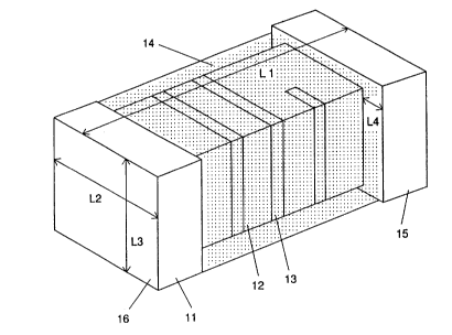
Figs. 1 and 2 are a perspective view and a
side view showing an inductance device according to one
embodiment of the present invention, respectively.
In Fig. 1, reference numeral 11 denotes a base
produced by press-molding or extruding an insulating
material, or the like, and reference numeral 12 denotes a
conductor film deposited on the base 11. The conductor
film 12 is formed on the base 11 by plating or a vapor
deposition method such as sputtering. Reference numeral
13 denotes grooves which are disposed in the base 11 and
in the conductor film 12. They are formed by radiating a
laser beam, etc, to the conductor film 12 or by
mechanical method of applying a grinding wheel, etc.
Reference numeral 14 denotes a protective material coated
to the portions of the base 11 and the conductor film 12
at which the grooves 13 are defined. Reference numerals
CA 02205634 1999-08-25
- 5 -
15 and 16 denote terminal portions each equipped with a
terminal electrode. The grooves 13 and the protective
material 14 are interposed between these terminal
portions 15 and 16. Incidentally, Fig. 2 is a side view
in which a part of the protective material 14 is cut
away.
The inductance device according to this
embodiment is practically adapted to a high frequency
range up to 1 - 6 GHz and has a very small inductance of
not greater than 50 nH. Moreover, the inductance device
preferably has a length L1, a width L2 and a height L3 as
follows
L1 - 0.5 to 1.5 mm (preferably, 0.6 to 1.1 mm and
further preferably, 0.6 to 1.0 mm)
L2 - 0.2 to 0.7 mm (preferably, 0.3 to 0.6 mm)
L3 = 0.2 to 0.7 mm (preferably, 0.3 to 0.6 mm)
When I,1 is smaller than 0.5 mm, both of the
self-resonance frequency f0 and the Q value drop and
excellent characteristics cannot be obtained. When L1
exceeds 1.5 mm, on the other hand, the device itself
becomes great in size. In consequence, the circuit board
for mounting electronic components, etc, (hereinafter
called the "circuit board" for short) cannot be
miniaturized and eventually, the electronic appliance
having the circuit board mounted thereto cannot be
miniaturized, either. When both of L2 and L3 are smaller
than 0.2 mm, the mechanical strength of the device itself
becomes so low that when the device is mounted on the
circuit board, etc, by using a mounting machine, device
- CA 02205634 1999-08-25
- 6 -
breakage is likely to occur. When L2 and L3 exceed 0.7
mm, on the other hand, the device becomes so great in
size that the circuit board and eventually the appliance
cannot be miniaturized. Incidentally, L4 (depth of
gradation) is preferably from 5 to 50 um. When L4 is
smaller than 5 um, the thickness of the protective
material 14 must be reduced and excellent protection
performance cannot be obtained. When L4 exceeds 50 um,
on the other hand, the mechanical strength of the base
becomes low and device breakage, etc, is also likely to
occur.
Each part of the inductance device having such
a construction will be explained in detail. Fig. 3 is a
sectional view of the base on which the conductor film is
formed, and Figs. 4 (a) and (b) are a side view and a
bottom view of the base, respectively.
To begin with, the shape of the base 11 will
be explained.
As shown in Figs. 3 and 4, the base 11
comprises a center portion lla having a rectangular
section so as to insure easy packaging to the circuit
board and end portions llb and llc integrally disposed at
both ends of the center portion lla and each having a
rectangular section. Though the end portions llb and llc
and the center portionlla have a rectangular section in
this embodiment, they may have a polygonal section such
as a pentagonal or hexagonal section. The center portion
lla is recessed from the end portions llb and llc. In
CA 02205634 1999-08-25
_ 7 _
this embodiment, since the end portions llb and llc have
a substantially square sectional shape, fittability of
the inductance device to the circuit board can be
improved, and since the grooves 13 are defined
transversely in the center portion lla, the base 11 has
no directivity in whichever way it may be mounted on the
circuit board. Therefore, its handling becomes easy. A
device portion (grooves 13 and protective material 14) is
formed at the center portion lla while the terminal
portions 15 and 16 are formed at the end portions llb and
11C.
Though the center portion lla and the end
portions llb and llc have a substantially square
sectional shape in this embodiment, they may have a
regular polygonal sectional shape such as a regular
pentagonal section. Furthermore, though the center
portion lla and the end portions llc and llb have the
same sectional shape, e.g. the square sectional shape,
they may be different. For example, the end portions llb
and llc have a regular polygonal sectional shape while
the center portion lla has another polygonal sectional
shape or a round sectional shape. When the sectional
shape of the center portion lla is round, the grooves 13
can be formed satisfactorily.
The center portion lla is recessed from the
end portions llb and llc in this embodiment so that when
the protective material 14 is applied, its contact with
the circuit board, etc, can be prevented. However, the
CA 02205634 1999-08-25
_ g _
center portion lla need not be recessed depending on the
thickness of the protective material 14 and the situation
of the circuit board (when a groove is formed at the
mounting portion of the circuit board or when the
electrode portion of the circuit board swells up). If
the center portion lla is not recessed from the end
portions llb and llc, the structure of the base 11
becomes simpler, productivity can be improved and
furthermore, the mechanical strength of the center
portion lla can be improved. In the case where the
recess is not formed, the base 11 also may have a square
pole shape having a rectangular section or a prism having
a polygonal section.
The heights Z1 and Z2 of the end portions of
the base 11 as shown in Fig. 4 (a) preferably satisfy
the following condition:
~Z1 - Z2~ <_ 80 pm (preferably, 50 um)
When the difference between Z1 and Z2 exceeds
80 um (preferably, 50 um), the device is attracted
towards one of the end portions by the surface tension of
the solder, etc, when the device is mounted on the
circuit board and fitted to the circuit board by the
solder, and in this case, the possibility of the so-
called "Manhattan phenomenon" in which the device stands
upright becomes extremely high. Fig. 5 shows this
Manhattan phenomenon. As shown in Fig. 5, the inductance
device is disposed on the circuit board 200 and the
solders 201 and 202 are sandwiched between the terminal
CA 02205634 1999-08-25
_ g _
portion 15 and the circuit board 200 and between the
terminal portion 16 and the circuit board 200,
respectively. When these solders 201 and 202 are molten
by reflow, etc, the surface tensions of the molten
solders 201 and 202 become different between the terminal
portions 15 and 16 due to the difference of their
application quantities, the difference of their melting
point resulting from the difference of the materials,
etc, so that the device turns with one of the end
portions (terminal portion 15 in Fig. 5) being the center
and stands upright as shown in Fig. 5. When the
difference of the height of Z1 and Z2 exceeds 80 pm
(preferably, 50 pm), the device is disposed under the
inclined state on the circuit board 200 and this
arrangement promotes stand-up of the device. The
Manhattan phenomenon occurs particularly remarkably in a
small and light-weight chip type electronic component
(inclusive of a chip type inductance device), and as one
of the factors for the occurrence of this Manhattan
phenomenon, the arrangement of the device under the
inclined state on the circuit board 200 due to the
difference of height between the terminal portions 15 and
16 is particularly taken into consideration. As a result,
the occurrence of the Manhattan phenomenon can be
drastically restricted by shaping the base 11 in such a
fashion that the difference of height between Zl and Z2
is not greater than 80 um (preferably, 50 pm). The
occurrence of the Manhattan phenomenon can be suppressed
w
CA 02205634 1999-08-25
- 10 -
substantially completely by limiting the difference of
height between Z1 and Z2 to not greater than 50 pm.
Next, chamfering of the base 11 will be
explained.
Fig. 6 is a perspective view of the base used
for the inductance device according to one embodiment of
the present invention. As shown in Fig. 6, corners lle
and lld of the end portions llb and llc of the base 11
are chamfered, and the radius R1 of curvature of each of
the chamfered corners lle and lld and the radius R2 of
curvature of the corner llf of the center portion lla are
preferably shaped to satisfy the following relation:
0.03 < R1 < 0.15 (unit: mm)
0.01 < R2 (unit: mm)
When R1 is smaller than 0.03 mm, each of the
corners lle and lld is pointed and is likely to crack
even due to a small impact, and deterioration of
performance is likely to develop due to such a crack.
When R1 exceeds 0.15 mm, the corners lle and lld are
rounded so much that the Manhattan phenomenon is more
likely to occur. When R2 is smaller than 0.01 mm, fins
are likely to occur at the corner llf, and the thickness
of the conductor film 12, which is formed on the center
portion lla and greatly governs performance of the
device, becomes greatly different between the corner llf
and the flat portion so that variance of the device
characteristics becomes great.
Next, the constituent materials of the base 11
CA 02205634 1999-08-25
- 11 -
will be explained. The constituent materials of the base
11 preferably satisfy the following characteristics:
volume resistivity: 1013 (preferably, 1014) or more
thermal expansion coefficient:
5 x 10-' (preferably, 2 x 10⁻⁵) or less at 20 to
500°C
dielectric constant: 12 (preferably, 10) or less
at 1 MHz
bending strength: 1,300 kg/cmz (preferably, 2,000
kg/cm2 ) or more
density: 2 to 5 g/cm3 (preferably, 3 to 4 g/cm3)
When the volume resistivity of the constituent
materials of the base 11 is smaller than 1013, a
predetermined current starts flowing through the base 11,
too, with the conductor film 12, and a parallel circuit
is formed. Therefore, the self-resonance frequency f0
and the Q value drop, and as a result, the device is not
suitable to a high frequency use.
When the thermal expansion coefficient exceeds
5 x 10⁻⁴, cracks are likely to develop in the base 11 due
to heat shock, etc. In detail, when the thermal
expansion coefficient is greater than 5 x 10-', the base
11 locally attains a high temperature because the laser
beam or the grinding wheel is used to form the grooves 13
as already described. This occurrence of the cracks can
be drastically restricted when the thermal expansion
coefficient satisfies the requirement described above.
When the dielectric constant is greater than
~r
CA 02205634 1997-OS-16
- 12 -
12 at 1 MHz, the self-resonance frequency f0 and the Q
value drop, so that the device is not suitable as a high
frequency device.
When the bending strength is smaller than
1,300 kg/cm2, device breakage, etc, sometimes occurs when
the device is mounted on the circuit board by using the
mounting apparatus.
When the density is smaller than 2 g/cm3, the
water absorbing capacity of the base 11 becomes so high
that its characteristics are extremely deteriorated and
device performance drops. When the density exceeds 5
g/cm3, the weight of the substrate becomes great and
problems occur in the mounting property, and so forth.
Particularly when the density is limited to the range
described above, the water absorbing capacity is small,
intrusion of water into the base 11 hardly occurs, the
base becomes light in weight, and no problem occurs, in
particular, when the device is mounted on the circuit
board by a chip mounter.
When the volume resistivity, the thermal
expansion coefficient, the dielectric constant, the
bending strength and the density of the base 11 are
limited as described above, the self-resonance frequency
f0 and the Q value do not drop, and the device can be
used as a high frequency device. Furthermore, because
the occurrence of cracks due to the heat shock, etc, in
the base 11 can be restricted, a defect ratio can be
reduced. Because the mechanical strength can be
CA 02205634 1999-08-25
- 13 -
improved, the device can be mounted on the circuit board,
etc, by using the mounting machine and productivity can
be improved.
Examples of the materials that can acquire
various characteristics described above are ceramic
materials consisting of alumina as the principal
components. However, these characteristics cannot be
obtained always by merely using the ceramic materials
consisting principally of alumina. In other words, since
these characteristics vary with the press pressure for
molding the base, the baking temperature and the
additives, the production condition must be suitably
adjusted. As an example of the concrete production
condition , the press pressure is 2 to 5 tons (2,000 to S,OOOkg) at a time
of shaping of the base 11, the baking temperature is
1,500 to 1,600°C and the baking time is 1 to 3 hours.
Concrete examples of the alumina materials are at least
92 wt$ of AILz03, not greater than 6 wt o of SiOz, not
greater than 1.5 wt~ of MgO, not greater than O.lo of
FeZ03, not greater than 0.3 wt~ of NazO, and so forth.
Next, the surface coarseness of the base 11
will be explained. The term "surface coarseness" used in
the following description means mean coarseness at the
center line, and the term "coarseness" used for the
explanation of the conductor film 12 also means mean
coarseness at the center line.
The surface coarseness of the base 11 is about
0.15 to about 0.5 pm, preferably about 0.2 to about 0.3
CA 02205634 1999-08-25
-14 -
~,cm. Fig. 7 is a graph showing the relation between the
surface coarseness of the base 11 and a peeling occurrence
ratio and shows the result of the following experiment.
The base 11 and the conductor film 12 are made of alumina
and copper, respectively, and samples are produced by
variously changing the surface coarseness of the base 11.
The conductor film 12 is formed on each sample under the
same condition. After each sample is washed by an
ultrasonic wave process, the surface of the conductor film
12 is examined so as to measure the existence of any
peeling. The surface coarseness of the base 11 is
measured by a surface coarseness meter (produced by Tokyo
Seimitsu Surfcom K.K., Model 574A) having a distal end R
of 5 ,um. As can be appreciated from the graph, when the
mean surface coarseness is not smaller than 0.15 ,um, the
occurrence ratio of peel of the conductor film 12 formed
on the base 11 is about 5%, and a good bonding strength
can be obtained between the base 11 and the conductor film
12. When the surface coarseness is greater than 0.2
,um, further, peeling of the conductor film 12 hardly
occurs. Therefore, the surface coarseness of the base 11
is preferably at least 0.2 ,um, if possible. Because
peeling of the conductor film 12 is one of the greatest
factors of deterioration of various characteristics, the
peel occurrence ratio is preferably not greater than 5%
from the aspect of the production yield, etc.
Fig. 8 is a graph showing the relation
between the frequency F and the Q value taking as a
parameter the
CA 02205634 1997-OS-16
- 15 -
surface coarseness of the base, and shows the result of
the following experiment. First, samples of the bases 11
having a coarseness of 0.1 dam or less, a surface
coarseness of 0.2 to 0.3 um and a surface coarseness of
0.5 um or more, respectively, are produced, and the
conductor film made of the same material (copper) and
having the same thickness is formed on each sample. The
Q value of each sample at a predetermined frequency F is
measured. As can be seen from Fig. 8, the drop of the Q
value, which presumably results from the deterioration of
the film structure of the conductor film 12, is observed
when the, surface coarseness of the base 11 is greater
than 0.5 um, and deterioration of the Q value is
remarkable particularly in the high frequency range. The
self-resonance frequency f0 (maximum value of each line)
also shifts towards the low frequency side when the
surface coarseness of the base 11 is 0.5 dam or more.
From the aspects of the Q value and the self-resonance
frequency f0, therefore, the surface coarseness of the
base 11 is preferably not greater than 0.5 um.
As described above, judging from the adhesion
strength between the conductor film 12 and the base 11
and from the result of both of the Q value and self-
resonance frequency f0 of the conductor film, the surface
coarseness of the base is preferably 0.15 to 0.5 um and
further preferably, 0.2 to 0.3 um.
The surface coarseness at the end portions llb
and llc is preferably different from that of the center
CA 02205634 1999-08-25
- 16 -
portion lla. In other words, the mean surface coarseness
at the end portions llb and llc is preferably smaller
than that of the center portion lla within the mean
surface coarseness range of 0.15 to 0.5 pm. Because the
terminal portions 15 and 16 are constituted by laminating
the conductor film 12 at the end portions llb and llc,
the surface coarseness of the conductor film 12 formed on
the end portions llb and llc can be reduced by making the
surface coarseness of the end portions llb and llc
smaller than that of the center portion lla. In this
way, adhesion with the electrode of the circuit
substrate, etc, can be improved, and the circuit board
and the inductance device can be bonded more reliably.
Because the grooves 13 are formed by laminating the
conductor film 12 at the center portion lla, the adhesion
strength between the conductor film 12 and the base 11
must be improved lest the conductor film 12 peel off
from the base 11 when the grooves 13 are formed by the
laser beam, etc. For this reason, the surface coarseness
of the center portion lla is preferably greater than that
of the end portions llb and llc. Particularly when the
grooves 13 are formed by the laser, the temperature rises
more drastically at the portion to which the laser is
radiated than the other portions, and the conductor film
12 sometimes peels due to the heat shock, etc. When the
grooves 13 are formed by the laser, therefore, the
bonding density must be improved much more between the
conductor film 12 and the substrate 11 than at other
CA 02205634 1997-OS-16
- 17 -
portions.
When the surface coarseness is made different
between the center portion lla and the end portions llb
and llc in this way, adhesion with the circuit board,
etc, can be improved and peel of the conductor film 12 at
the time of processing of the grooves 13 can be
prevented.
In this embodiment, the bonding strength
between the conductor film 12 and the base is improved by
adjusting the surface coarseness of the base 11, but it
can be improved without adjusting the surface coarseness,
for example, by disposing an intermediate layer made of
Cr alone or an alloy of Cr with other metals between the
base 11 and the conductor film 12. Needless to say, a
higher adhesion strength can be obtained between the
conductor film 12 and the base 11 by adjusting the
surface coarseness of the base 11 and moreover,
laminating the intermediate layer and the conductor film
12 on the base 11.
Next, the conductor film 12 will be explained.
The conductor film 12 preferably has a very
small inductance of 50 nH or less, a Q value of at least
at a radio frequency signal of 800 MHz or more and
further, a self-resonance frequency of 1 to 6 GHz. The
25 materials and the production method must be selected
appropriately to obtain the conductor film 12 having such
characteristics.
Hereinafter, the conductor film 12 will be
CA 02205634 1999-08-25
- 18 -
explained more concretely.
The constituent materials of the conductor
film 12 are electrically conductive materials such as
copper, silver, gold, nickel, and so forth.
Predetermined elements may be added to copper, silver,
gold, nickel, etc, so as to improve the weather
resistance. Alloys between the conductive materials and
non-metallic materials may be used, too. Copper and its
alloys are used in most cases as the constituent
materials from the aspects of the production cost, the
weather resistance and easiness of production. When
copper or the like is used as the material of the
conductor film 12, a foundation film is first formed on
the base 11 by electroless plating and a predetermined
copper film is then formed on the foundatl011 flllll by
electroplating to provide the conductor film 12. When
the alloys are used to form the conductor film 12,
sputtering or vapor deposition is preferably used for
forming the conductor film 12. When copper and its
alloys are used as the constituent materials, the
formation thickness of the conductor film 12 is
preferably at least 15 Vim. When the thickness is smaller
than 15 um, the Q value of the conductor film 12 becomes
so great that predetermined characteristics cannot be
obtained so easily. Fig. 9 is a graph showing the
relation between the film thickness of the conductor film
12 and the Q value when an inductance is 10 nH. The Q
values are measured by using copper as the constituent
CA 02205634 1999-08-25
- 19 -
material of the conductor film 12 and changing the
thickness of the conductor film 12 formed on the base 11
while the material of the base 11, its surface
coarseness, etc, are kept under the same condition. As
can be seen from Fig. 9, the Q value exceeds 30 when the
thickness of the conductor film 12 is at least 21 um.
Therefore, the thickness of the conductor film 12 is
preferably at least 21~,m. Because the Q value cannot be
much improved within the range of the thickness of the
conductor film 12 exceeding 35 Vim, the thickness is
preferably not greater than 35 ~,m from the aspect of the
production cost and to reduce the defect ratio.
The conductor film 12 may have a single-
layered structure or a multi-layered structure. In other
words, a plurality of conductor films made of different
constituent materials may be laminated to produce the
conductor film 12. For example, corrosion of copper can
be prevented by forming first a copper film on the base 11
and then laminating a metal film (nickel, etc) having a
good weather resistance, though the weather resistance is
not fully satisfactory.
The methods of forming the conductor film 12
include plating (electroplating and electroless plating),
sputtering, vapor deposition, and so forth. Among them,
plating has gained a wide application because it has high
productivity and provides less variance in the film
thickness.
The surface coarseness of the conductor film
I
CA 02205634 1999-08-25
- 20 -
12 is preferably not greater than 1 um and further
preferably, not greater than 0.2 um. When the surface
coarseness of the conductor film 12 exceeds 1 um, the Q
value at a high frequency drops due to the skin effect,
Fig. 10 is a graph showing the relation between the
frequency F and the Q value taking the surface thickness
of the conductor film 12 as a parameter. The result
shown in Fig. 10 is plotted on the basis of the following
experiment. First, conductor films 12 are formed by
changing the surface coarseness on the bases 11 having
the same size, made of the same material and having the
same surface coarseness, and the Q value at each
frequency of each sample is measured. As can be seen
from Fig. 10, the Q value becomes small in the high
frequency range when the surface coarseness of the
conductor film 12 is greater than 1 pm. It can be also
appreciated from Fig. 10 that when the surface coarseness
of the conductor film 12 is not greater than 0.2 um, the
Q value in the high frequency range, in particular,
becomes extremely high.
As described above, the surface coarseness of
the conductor film 12 is preferably not greater than 1.0
um and further preferably, not greater than 0.2 pm. When
this condition is. satisfied, the skin effect of the .
conductor film 12 can be reduced, and the Q value in the
high frequency range, in particular, can be improved.
The adhesion strength between the conductor
film 12 and the base 11 is preferably such that when the
CA 02205634 1999-08-25
- 21 -
base 11 having the conductor film 12 formed thereon is
left standing for several seconds at a temperature of
400°C, the conductor film 12 is not peeled from the base
11. When the device is packaged to the substrate, etc,
the device undergoes self exothermal or heat from other
members is applied to the device, so that a temperature
of not lower than 200°C is applied in some cases to the
device. Therefore, if the conductor film 12 is not
peeled from the base 11 at 400°C, deterioration of the
device characteristics does not occur even when heat is
applied to the device.
Next, the protective material 14 will be
explained.
Organic materials having excellent weather
resistance and materials having an insulating property
such as an epoxy resin are used for the protective
material 14. The protective material 14 preferably has
transparency such that the condition of the grooves 13,
etc, can be observed. Further, the protective material
14 preferably keeps it's transparency. When the protective
material 14 is colored in red, blue, green, etc, different
from the colors of the conductor film 12 and the terminal
portions 15 and 16, each portion of the device can be easily
distinguished from others and inspection of each device
portion can be carried out easily. When the color of the
protective material 14 is changed in accordance with the
size of the device, its characteristics, its type number,
CA 02205634 1999-08-25
- 22 -
etc, the mistake of fitting the devices having different
characteristics, type numbers, etc, to wrong portions can
be reduced.
The protective material 14 is applied
preferably in such a fashion that the length Z1 from the
corner portions 13a of the grooves 13 to the surface of
the protective material 14 is at least 5 pm as shown in
Fig. 11. When Zl is smaller than 5 um, deterioration of
the characteristics and discharge are likely to develop,
and the characteristics of the device might drop
drastically. The corner portions 13a of the grooves 13
are those portions at which discharge, etc, is
particularly likely to develop, and the protective
material 14 having a thickness of at least 5 um is
deposited extremely preferably on the corner portions
13a. Electrode films, etc, are formed in some cases by
again applying plating after the protective material 14
is formed, and unless the protective material 14 having a
thickness of at least 5 pm is formed on the corner
portions 13a, the electrode film, etc, is directly formed
on the protective material 14 which invites disadvantages
if the electrode fails, etc, adheres thereto, and
deterioration of the characteristics occur.
Next, the terminal portions 15 and 16 will be
explained.
Though the terminal portions 15 and 16 are
allowed to function sufficiently even by the conductor
film 12 alone, in order to let them cope with various
CA 02205634 1997-OS-16
- 23 -
environments and conditions, a multi-layered structure is
preferably employed.
Fig. 12 is a sectional view of the terminal
portion 15. In Fig. 12, the conductor film 12 is shown
formed on the end portion llb of the base 11, and a
protective layer 300 made of a material having the
weather resistance such as nickel, titanium, etc, is
formed on the conductor film 12. A bonding layer 301
made of a solder, etc, is further formed on the
protective layer 300. The protective layer 300 improves
the bonding strength between the bonding layer and the
conductor film 12 and the weather resistance of the
conductor film. In this embodiment, either nickel or a
nickel alloy is used as the constituent material of the
protective layer 300, and the solder is used as the
constituent material of the bonding layer 301. The
thickness of the protective layer 300 (nickel) is
preferably 2 to 7 um. When the thickness is smaller than
2 um, the weather resistance drops and when it exceeds 7
um, the electric resistance of the protective layer 300
(nickel) itself becomes so great that the device
characteristics are remarkably deteriorated. The
thickness of the bonding layer 301 (solder) is preferably
5 to 10 um. When the thickness is smaller than 5 um, the
bonding layer 301 is apt to be lost in the soldering
process (soldering defect) and satisfactory bonding
between the device and the circuit board cannot be
expected. When the thickness exceeds 10 um, the
CA 02205634 1999-08-25
- 24 -
Manhattan phenomenon is more likely to occur, and
mounting ability drops remarkably.
The inductance device constituted in the way
described above is free from deterioration of the
characteristics but has extremely high mounting ability
and productivity.
Next, the production method of this inductance
device will be explained.
First, the base 11 is produced by press-
molding or extruding an insulating material such as
alumina. The conductor film 12 is then formed on the
base 11 as a whole by plating or sputtering. The spiral
grooves 13 are formed on the base 11 on which the
conductor film 12 is deposited. These grooves 13 are
formed by laser processing or cutting. Since laser
processing has extremely high productivity, the
explanation will be given on this method. First, the
base 11 is fitted to a rotary machine and while the base
11 is rotated, a laser beam is radiated to the center
portion lla of the base 11 to remove both of the
conductor film 12 and the base and to thereby form the
spiral grooves. YAG laser, excimer laser, carbonic acid
gas laser, etc, can be employed in this case. The laser
beam is contracted by a lens, etc, and is radiated to the.
center portion lla of the base 11. Further, the depth of
the grooves 13, etc, can be adjusted by adjusting power
of laser and the width of the grooves 13, etc, can be
adjusted by exchanging the lens used for contracting the
CA 02205634 1999-08-25
- 25 -
laser beam. Since absorptivity of the laser is different
depending on the constituent materials of the conductor
film 12, etc, the kind of the laser (wavelength of laser)
is preferably and appropriately selected in accordance
with the constituent materials of the conductor film 12.
After the grooves 13 are formed, the
protective material 14 is applied to the portions where
the grooves 13 are formed (center portion lla), and is
then dried.
A product can be completed at this stage, but
the nickel layer and the solder layer are laminated
particularly on the end portions 15 and 16 so as to
improve the weather resistance and bondability. The
nickel layer and the solder layer are formed on the semi-
finished product having the protective material 14 formed
thereon, by plating, or the like.
Though this embodiment has been explained
about the inductance device, similar effects can be
likewise obtained for those electronic components which
have the conductor film formed on the base made of an
insulating material.
Figs. 13 and 14 show a wireless terminal
equipment according to an embodiment of the present
invention. In these drawings, reference numeral 29
denotes a microphone for converting sound to audio
signals, reference numeral 30 denotes a speaker for
converting the audio signals to the sound, reference
numeral 31 denotes an operation portion comprising dial
CA 02205634 1997-OS-16
- 26 -
buttons, etc, reference numeral 32 denotes a display
portion for displaying a call, etc, reference numeral 33
denotes an antenna and reference numeral 34 denotes a
transmission portion for demodulating the audio signals
from the microphone 29 and converting them to
transmission signals. The transmission signals generated
by the transmission portion 34 are emitted outside
through the antenna. Reference numeral 35 denotes a
reception portion for converting the reception signals
received by the antenna to the audio signals. The audio
signals generated by the reception portion 35 are
converted to the sound by the speaker 30. Reference
numeral 36 denotes a control portion for controlling the
transmission portion 34, the reception portion 35, the
operation portion 31 and the display portion 32.
Next, an example of its operation will be
explained.
When a call is received, a call signal is sent
from the reception portion 35 to the control portion 36
and the control portion 36 causes the display portion 32
to display predetermined characters, etc, on the basis of
the call signal. When a button, etc, representing that
the call is received from the operation portion is
pushed, the signal is sent to the control portion 36.
Receiving this signal, the control portion 36 sets each
portion to the call mode. In other words, the signal
received by the antenna 33 is converted to the audio
signal by the reception portion 35, the audio signal is
CA 02205634 1997-OS-16
- 27 -
output as the sound from the speaker 30, the sound
inputted from the microphone 29 is converted to the sound
signal, and the signal is then emitted outside through
the transmission portion 34 and the antenna 33.
Next, operation of transmission will be
explained.
In the transmission mode, the signal
representing transmission is input from the operation
portion 31 to the control portion 36. When the signal
corresponding to the telephone number is subsequently
sent from the operation portion 31 to the control portion
36, the control portion 36 transmits the signal
corresponding to the telephone number from the
transmission portion 34 through the antenna 33. When the
communication with the receiving party is established by
this transmission signal, the signal representing the
communication is sent from the reception portion 35 to
the control portion 36, and the control portion 36 sets
each portion to the transmission mode. In other words,
the signal received by the antenna 33 is converted by the
reception portion 35 to the audio signal and this signal
is output as the sound from the speaker 30. The sound
inputted from the microphone 29 is converted to the audio
signal and is transmitted outside from the transmission
portion 34 through the antenna 33.
The inductance device explained above (shown
in Figs. 1 to 12) is used for a filter circuit or a
matching circuit inside the transmission portion 34 and
CA 02205634 1999-08-25
- 28 -
the reception portion 35, and several to dozens of such
inductance devices are used in one wireless terminal
equipment. Because the circuit board, etc, used inside
the equipment can be miniaturized by using such
inductance devices, the size of the equipment itself can
be reduced, too. Moreover, because the problems such as
device breakage can be prevented, the defect ratio can
be reduced and productivity can be improved.