Note: Descriptions are shown in the official language in which they were submitted.
CA 0220~733 1997-0~-20
BACKGROUND OF THE INVENTION
1. Field of the Invention
The present invention relates to the field of integrated
circuit design, specifically to redundancy circuits used to
increase the production yield of non-volatile memory
integrated circuits.
2. Prior Art
Particle defects due to fabrication environments can
cause non-volatile memory integrated circuits, especially
those with high density memory arrays, to fail. As a result,
a yield loss in final production test is realized, causing
the final satisfactory product to cost substantially more so
as to cover the cost of the faulty parts. To help increase
the yield, a technique commonly known as redundancy repair
(row, column, or block), is used to avoid use of the failed
memory portion in favor of a corresponding redundant memory
portion included on the integrated circuit just for such
purposes, should it be needed.
Redundancy circuits typically store the addresses of the
failed memory portion in some form of storage, and in use,
compare the incoming addresses versus the stored redundancy
addresses for a match. If a match is found, the redundancy
array is enabled and the main array is disabled. An enable
042236 . P026 -1- RWB/ jm
CA 0220~733 1997-0~-20
fuse is typically included to enable or disable the
redundancy addresses. Some conventional implementations use
a resistor fuse as a programmable element to store the failed
addresses. The fuse is blown by applying a high current
through the fuse by a test enabling circuit. Such a fuse is
one-time programmable only. Since the current required to
blow the fuse is normally high, the transfer switch has to be
large, and requires a correspondingly large chip area.
Other implementations use EPROM technology (erasable
programmable read-only memory). However, as implemented, an
EPROM fuse is also one-time programmable. Further, an EPROM
requires complicated shielding over the fuse after
programming in order to retain the programming charge. Other
implementations use EEPROM (electrically erasable
programmable read only memory) in an inverter mode (as
commonly known), i.e., the cell in the read mode acts as a
current sink for some loading elements such as a PMOS, NMOS,
or a resistor. The device gate is typically held at 2V and
its source at ground, with its drain coupled to the load.
The voltage at the loading element is the output of the
memory cell.
Prior art implementations for a memory cell row repair
normally include a separate redundancy row decoder and an
enable/disable fuse for each redundancy row. Prior art
implementations for the row repair also normally include a
redundancy row decoder which is different from the regular
04223 6 . P02 6 -2- RWB/ jm
CA 0220~733 1997-0~-20
row decoder. Further, prior art implementations also require
a separate high voltage decoder for programming each fuse
element. All these require additional circuits and added
complexity to achieve the desired result.
- In prior art U.S. Patent No. 4,617,651 by W. Ip and G.
Perlegos and U.S. Patent No. 4,538,245 by G. Smarandolu and
G. Perlegos, a redundancy disable/enable circuit is required
for each redundant row. In the present invention, out-of-
bound addressing is used to self enable a redundant row,
thereby eliminating the need for a redundant disable/enable
circuit. Moreover, in both the '651 and '245 patents, the
redundancy element is a one time programmable fuse. However,
the EEPROM fuse in the present invention enables the
redundancy to be programmable many times and eliminates the
need for high current devices required to burn the one time
programmable fuse. Finally, in the '651 and ~245 patents, a
separate redundancy programming circuit is required whereas
in the present invention, the programming circuit is shared
with the normal programming circuit through the use of column
switches.
042236 . P026 -3- RWB/ jm
CA 0220~733 1997-0~-20
SUMMARY OF THE INVENTION
The present invention includes a redundancy predecoder
circuit, a source follower EEPROM memory fuse, a scheme to
use the column high voltage drivers (also known as page
latch) to program the EEPROM fuses, a scheme to use the
regular row decoder (also known as wordline decoder or x-
decoder) as the redundancy row decoder, and an out-of-bounds
address for the fuses as a redundant enable/disable signal.
The redundancy predecoder circuit is used to adapt the
regular row predecoder for use with the redundancy row
decoder to minimize the additional circuits required to
implement the redundancy. The regular column high voltage
drivers are used to program the EEPROM fuses to mi n i mi ze the
need for additional high voltage drivers for the redundancy
circuits. A high voltage test signal is enabled during
manufacturing to enable the transfer switches between the
regular column drivers and the EEPROM fuses, and can be used
to disable the main row decoders in order to avoid
programming the regular memory cells. Moreover, since the
main row decoder and the redundancy row decoder are
identical, the layout of the two match exactly, and no
additional effort is required for the layout of redundancy
row decoders.
The EEPROM fuses are initially set at an out-of-bound
address (that is, higher than the maximum address of the main
042236 . P026 -4- RWB/ jm
CA 0220~733 1997-0~-20
array) so that the redundancy rows are initially "disabled~
by not being within the normally used address range.
Additionally, any redundancy row can also be disabled by
programming an out-of-bound address into the corresponding
EEPROM fuse. Note that the maximum number of addresses that
can be addressed by the address inputs is larger than the
address space required by the main memory array. By
reserving a certain number or block of addresses to be
"invalid" addresses not usually input to the device, the
redundant address fuses can be initialized to one of the
unused addresses and redundancy is not invoked until the fuse
is programmed with a "valid" address. Thus, the redundancy
scheme does not require separate circuits to enable or
disable redundant rows, but instead is enabled automatically
when fuses are programmed with the address of a faulty row.
The EEPROM fuse is a source follower type memory cell
used with a MOS differential comparator. The source follower
EEPROM cell in the read mode has its gate and its source
coupled to a regulated voltage and its drain connected to a
current bias which is connected to ground. The drain voltage
is the output of the memory cell.
0~2236.P026 -5- RWB/ jm
CA 0220~733 1997-0~-20
BRIEF DESCRIPTION OF THE FIGURES
Figure 1 is a block diagram for the preferred embodiment
of the redundancy circuit of the present invention.
Figure 2 is a circuit diagram of the row decoders of
Figure 1.
Figure 3 is a circuit diagram of the row predecoders of
Figure 1.
Figure 4 consisting of Figures 4a and 4b is a circuit
diagram of a typical comparator circuit of Figure 1.
Figure 5 is a circuit diagram of an EEPROM fuse of
Figure 1.
04223 6 . P02 6 -6 - RWB/ jm
CA 0220~733 1997-0~-20
DETAILED DESCRIPTION OF THE PRESENT INVENTION
An apparatus and method for a redundancy circuit used in
a non-volatile memory chip to increase the production yield
due to manufacturing defects is described in detail. The
-description will assume that the memory is an analog non-
volatile memory of the type used in analog recording and
playback devices manufactured and sold by Information Storage
Devices, Inc. of San Jose, California, as that is the
intended application of the preferred embodiment. However,
the invention may equally as well be used in other storage
systems such as digital storage systems. An analog non-
volatile memory cell can typically store a single sample of
an analog signal with a resolution of approximately one part
in 250. For an audio application with 60 seconds of storage
capacity, the array size will be 60 seconds divided by the
inverse of the audio sampling rate ( 8 KHZ is typical, giving
a sample every 125~sec), or 60 seconds/125~sec = 480K cells.
The 480K array in the preferred embodiment is divided into
1200 columns and 400 rows.
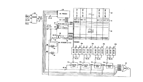
Now referring to Figure 1, a block diagram of a
preferred embodiment of the present invention may be seen.
Figure 1 includes a main memory 20, in this embodiment
comprising a main array of the 400 rows of memory cells
labeled ROW0 through ROW399, and a redundancy array below the
main array comprised of 4 rows of memory cells labeled RROW0
through RROW3, providing a total array of 404 identical rows
042236 . P026 -7- RWB/ jm
CA 0220~733 1997-0~-20
of memory cells. Each row of the array is divided into 12
scans, each scan being equal to 12.5 ms of recording and
playback, or for 8 KHz, 100 cells. For all 12 scans, this
represents 150 ms of recording and playback. In this
particular implementation, 150 ms is chosen to be the audio
time resolution, in that recording and playback of any signal
or message will be of a time equal to an integer multiple of
150 ms increments, regardless of when within the last 150 ms
the signal or message terminated. Thus the whole row can be
progra~med or read back in 12 scans, the incrementing from
one scan to the next being automatic. Thus addressing is
only required from row to row, the column addressing being
automatically advanced scan to scan. Since the column
drivers must drive 100 cells at a time, 100 column drivers 22
are used, each operating through a 12:1 MUX 24 to
controllably connect the 100 column drivers to a respective
100 columns of the 1200 columns for each of the respective 12
groups of 100 columns each (e.g. for each of the 12 scans per
row).
Also shown in Figure 1 is the row counter 26, the word
line or row predecoders 28, the row decoders 30, four
comparators 32 and four sets of EEPROM cells forming EEPROM
fuses 34. The EEPROM fuses are located directly below the
main array to facilitate the connection from the regular
columns to the EEPROM fuses. The row counter 26 operates
from a row clock ROWCLK to sequence through the rows by way
of a 9 bit address A8..A0 and its inverse A8/..A0/, though
042236 . P026 -8- RWB/ jm
CA 0220~733 1997-0~-20
can also receive a parallel input AIN..AI0 and an input
strobe signal PARLD to initially point the counter to any row
of the array. The word line predecoders 28 decode the least
significant three bits A2..A0 of the address to activate 1 of
8 select gate lines SG7..SGO. The remaining 6 bits of the
address A8/..A3 are decoded by appropriate choice of
connection of address lines and their inverses to 50 NAND
gates 3 6. The NAND gates combined with an 8:1 MUX minimize
the circuits so they can fit into the height dimension
(pitch) of the cell. The redundancy row decoder 38 is the
same as a regular row decoder except that all but one of the
inputs to the NAND gate 40 of the redundancy row decoder 38
are tied to VCC, so that that one input may itself control
the output of the NAND gate. The redundancy row decoding is
realized using the regular row predecoder signals SG0 through
SG3 with the addition of control signals COMR0-C0MR3 from the
comparators 32, together with certain control logic
hereinafter described in greater detail.
In general, except as altered by the present invention
as described herein, the row counter 26, and the combination
of the word line predecoders 2 8 and the word line or row
decoders 30, function as in the prior art ISD devices, and as
described in various issued patents, including U.S. Patent
No. 5, 241,494. Similarly, the output circuits, much of the
control of the analog storage device, and certain other
aspects of the device.are not shown in Figure 1 for clarity,
as these are also known from prior art ISD devices and issued
042236 . P026 -9- RWB/ jm
CA 0220~733 1997-0~-20
patents, and their inclusion herein would unnecessarily
obscure the present invention. (See U.S. Patent No.
4,890,259 for a general overview of this type of device.)
Initially after fabrication, the analog storage device
is tested to determine if any storage cells in the main array
and redundant array are bad (nonfunctional, usually by a
storage cell providing a fixed output at one voltage extreme
independent of its programming, though it is possible more
than one cell in a row or an entire row will be nonfunctional
for some reason). If a storage cell in the main array is
determined to be bad, the entire row of cells will be dropped
from use in favor of one of the 4 rows of redundant cells, as
subsequently described in greater detail. Typically, testing
to determine the number of bad rows, if any, would be done at
wafer sort to avoid packaging costs for the integrated
circuits which are faulty in ways that cannot be repaired by
use of the redundant rows. Then programming the fuses to cut
out faulty rows would typically be done after packaging to be
sure no further loss was incurred by packaging.
Once the device has been tested after packaging and the
location of the bad cells has been identified by row address
(in the embodiment disclosed the bad cells must not effect
more than 4 rows, the number of redundant storage cell rows
provided), the bad address EEPROM fuses 34 may be programmed.
Each bad row address is a 9 bit address, so that 9 EEPROM
fuses are required for each address, or 3 6 EEPROM fuses total
042236 . P026 -10- RWB/ jm
CA 0220~733 1997-0~-20
are needed to implement the 4 redundant rows. As shall be
subsequently seen, each EEPROM fuse in the preferred
embodiment uses two EEPROM cells which are independently
programmed to operate differentially. Consequently there are
i2 EEPROM cells to program to set the four 9-bit bad address
EEPROM fuses.
At the start of the programming cycle for the bad
address EEPROM cells, a test mode is entered by way of the
test enable signal, TESTHV, which will connect the columns to
the fuses. This signal can also be used to disable the cell
decode circuits 36 of the main array, though in the specific
embodiment disclosed, the main array is effectively disabled
by simply using an address that is out of the main array
address range. The column drivers 22 are serially loaded
with ones or zeros depending on the desired programmed or
erased state of a cell coupled to each driver. Since there
are 100 line drivers, each EEPROM cell of the four 9-bit bad
address EEPROM fuses may be coupled to a respective line
driver for a particular scan, in which case all four
redundancy row addresses are programmed using the same scan.
Alternatively each 18 EEPROM cells of a respective 9-bit bad
address EEPROM fuse may be coupled to a different scan
(different setting of the 12:1 MUXs 24) so that each 9-bit
bad address EEPROM fuse is programmed on a separate scan.
The choice of either of these or some other coupling is a
matter of design choice and chip layout, not important to the
subject of this disclosure.
042236 . P026 -11- RWB/ jm
CA 0220~733 l997-0~-20
The loaded data corresponds to the failed row addresses.
A high voltage, e.g. 21V, is applied to all column drivers to
start the programming cycle. The high voltage is such as
supplied from a standard charge pump. The same high voltage
is also applied to other required circuits, such as row
decoders and row predecoders. For each scan, the first scan
write cycle of 12.5 ms includes 1.25 ms allocated for the
erase cycle and 11.25 ms allocated for the write cycle. The
signal TESTHV is asserted to couple the EEPROM cells of the
fuses to the array columns. Also an out of range address
(above the address range for the 400 rows of the main memory
array, the maximum number of possible rows being addressable
from addresses A0-A8 being 512) is asserted on address lines
A8..A0 so that none of the rows of the main memory array are
addressed. Thus during an erase cycle for redundancy fuses,
only the EEPROM cells of the fuses are erased. Then the
erase cycle is disabled and the write cycle is enabled for
the remainder of the scan. During the write cycle, only
EEPROM cells of the fuses are programmed, specifically by
each of the column drivers outputting either a high voltage
or zero depending on the desired state of the respective
EEPROM cell of the fuse.
The 12:1 MUX may be serially enabled by the scan rate of
12.5 ms so that the process is repeated for the 12 scans,
though as stated before, in the exemplary embodiment, all
fuses can be programmed in a single scan if coupled to the
columns of the same scan during the programming.
042236 . P026 -12- RWB/ jm
CA 0220~733 l997-0~-20
Consequently the serial enabling of the 12 scans could be
eliminated if desired. Also, the fuses are initially loaded
with all ls at the time of fabrication in a manner to be
described, so as to automatically contain an out of main
memory range address.
With respect to the addressing during programming and
normal analog recording and playback device operation, at
least for rows of main memory array cells with no faults, the
output of NOR gate 42 will be high. Consequently the output
of AND gates 44 and 46 will be the same as the second inputs
thereto, namely the states of address A8 and A8/, so that the
presence of the AND gates in these two address lines will be
of no effect.
Once the fuses are programmed as described, then in
normal operation of the analog storage device, comparators 32
constantly compare the 9 bit faulty row address stored in the
fuses with the address on address lines A8..A0. When
addressing a faulty row of main memory is attempted, one of
the comparators will detect an address comparison and provide
a high output signal. Thus one of the inputs COMR3.. COMR0 to
NOR gate 42 will go high, driving the output of the NOR gate
low. Therefore, one of the inputs of the AND gates 44 and 46
will go low, forcing the output of the AND gates low
regardless of the state of A8 and A8/. Now at least one
input of all 50 NAND gates 36 will be low, holding the output
of all 50 NAND gates high, which as shall subsequently be
042236 . P026 -13- RWB/ jm
CA 0220~733 l997-0~-20
seen in detail, invalidates the address to every row of the
main array, effectively disabling the addressing of any row
of the main memory array.
The output of the NOR gate 42 is also coupled to the
inverter 48, so that when the output of the NOR gate goes low
upon a comparator detecting a comparison, the output of the
inverter 48 will go high, so that now all inputs of the NAND
gate 40 are high, enabling the addressing of the redundant
rows RROW3..RROW0. The addressing of the one of four
redundant rows is done by the predecoders 28 responding to
the output of the comparator finding an address match to
assert a corresponding one of signals SG3..SG0. Thus when a
faulty row of the main memory array is addressed, whether
during recording or playback, the corresponding redundant row
is addressed instead, all in a manner transparent to other
parts of the integrated circuit system and the outside world.
Figure 2 is a circuit diagram for a typical row decoder
of Figure 1. The inputs to the row decoders are SGO..SG7,
and as X8IN..X3IN, unique combinations of the address signals
A3..A8 and their inverses A3/..A8/. The row addresses are
input to the NAND gate for straight binary decoding from 1 to
50, together with the 8 inputs from the predecoder, thereby
decoding a total of 8 times 50 or 400 rows. The NAND gate 36
for each decoder receives a different combination of 6
address signals A8..A3 and their inverse A8/..A3/ so that one
and only one NAND gate will have all inputs high at the same
042236 . P026 -14- RWB/ jm
CA 0220~733 1997-0~-20
time. Thus normally the output of a NAND gate 36 will be
high. This holds high voltage switch 52 off through inverter
50, holding n-channel devices M9 through M16 off. (The high
voltage switch could be implemented using a clocked high
voltage or a high voltage level shifter as is well known in
the art.) The high output of NAND gate 36 also turns on N-
channel devices M1 through M8, coupling all eight rows
controlled by that decoder low.
When the specific combination of the 6 address signals
A8..A3 and their inverse A8/..A3/ for that row decoder are
all high at the same time, the output of a NAND gate 36 will
go low. This turns off N-channel devices M1 through M8, and
turns on high voltage switch 52 through inverter 50. The
output of the high voltage switch could be the high voltage
in programming mode, VCC or some intermediate level in read
mode (or zero when not selected). The high voltage output of
the switch turns on n-channel devices M9 through M16 to
couple each of ROW0 through ROW7 to a respective row
predecoded signal SG0 to SG7. Since only one of the lines
SG0 to SG7 will have a high voltage on it at any one time,
only one row of the seven rows is driven high.
Figure 3 is a circuit diagram for a row predecoder
circuit 28 of Figure 1. The row predecoder circuit comprises
two circuits: the MAIN ROW PREDECODER and the REDUNDANT ROW
PREDECODER. Referring first to the redundant row predecoder
of Figure 3, inverters 66 serve to invert the input address
042236.P026 -lS- RWs/jm
CA 0220~733 l997-0~-20
signals A2, A1 and A0, with inverter 68 reinverting the A2
signal. NOR gates 70, 72, 74, 76 and 78 and NAND gate 80
serve to decode the redundant rows using comparator outputs
COMRO through C0MR3. Note that since only one row address
(A8..A0) is active at any given time, no more than one
comparator output COMR0 through C0MR3 can be active at any
given time (usually none are active for most, if not all
addresses). For example, if none of the comparator outputs
COMR0 through COMR3 are active (high), the output of NOR gate
70 will be high, so that the output of NAND gate 80, X2B,
will be the inverse of the signal on the A2 address input
line. Also the outputs of the NOR gates 72 and 76 will be
the inverse of the outputs of the inverters 66 on the A1 and
A2 lines, with the outputs of NOR gates 74 and 78 being the
inverse of the outputs of NOR gates 72 and 76. Consequently,
if none of the comparator outputs COMR0 through COMR3 are
active, the outputs of gates 80, 74 and 78 are X2B, XlB and
XOB, the inverse of the signals on the address lines A2, A1
and A0, respectively.
When one of the comparators finds an address comparison,
its output will go high. If COMR0 is high and COMR1,2,3 are
low, the output of NOR gate 70 will be low, causing X2B, the
output of NAND gate 80 to be high. The output of NOR gate 72
will also be low, and since C0MR2,3 are low, the output of
NOR gate 74, XlB, will be high. The output of NOR gate 76
will also be low, and since COMR1,3 are low, the output of
04223 6 . P026 -16- RWB/ jm
CA 0220~733 l997-0~-20
NOR gate 78, XOB, will be high. Consequently, X2B,XlB,XOB =
111, regardless of the signals on the address lines A2-AO.
If COMRl is high and COMRO,2, 3 are low, the output of
NOR gate 70 will be low, causing the output of NAND gate 80,
-X2B, to be high. The output of NOR gate 72 also is also low,
and since COMR2, 3 are low, the output of NOR gate 74, XlB, is
high. Further, since COMRl is high, the output of NOR gate
78, XOB, equal low. Thus, X2B,XlB,XOB = 110, regardless of
the signals on the address lines A2-AO.
Continuing to refer to Figure 3, if C0MR2 is high and
COMRO,l, 3 are low, the output of NOR gate 70 will be low,
which causes the output of NAND gate 80 to be high. Further,
since COMR2 is high, the output of NOR gate 74, XlB, to be
low. Also the output of NOR gate 76 will be low, and since
COMRl, 3 are low, the output of NOR gate 78, XOB, will be
high. Thus, X2B,XlB,XOB = 101, regardless of the signals on
the address lines A2-AO. Finally, if COMR3 is high and
COMRO,1,2 are low, the output of NOR gate 70 will be low,
which causes the output of NAND gate 80 to be high. Also
since COMR3 is high, the output of NOR gate 74, XlB, will be
low and the output of NOR gate 78, XOB, will be low. Thus,
X2B,XlB,XOB = 100, regardless of the signals on the address
lines A2-AO. The row predecoder circuit of Figure 3 serves
as an example of four re~--n~nt rows only. However, in
another embodiment, more or fewer redundant rows can be used
042236 . P026 -17- RWB/ jm
CA 0220~733 l997-0~-20
Referring now to the main row predecoder of Figure 3,
inverters 54, 56, and 58 serve to invert the input signals to
the main row decoder X2B, XlB, and XOB, to provide the
signals X2I, XlI, and XOI respectively, with NAND gates 60
and inverters 62 providing straight binary decoding for the 3
inputs. The inputs to the main row predecoder X2B-XOB are
the inverse of the signals on the address lines A2-AO
respectively, when no redundancy is used (i.e. when
C0MR3..COMRO are all low). The 3-input NAND gates 60 and
inverters 62 are connected to decode from 1 to 8 using
address lines A2..AO when redundancy is not used. For
example if A2,Al,AO = 000, SGO is high and SGl..SG7 are all
low; if A2,Al,AO = 011, SG3 is high and SGO..SG2 and SG4..SG7
are all low, etc. Thus during the use of the redundancy, if
COMRO is high, X2B,XlB,XOB = 111, so that SGO is high. If
COMRl is high, X2B,XlB,XOB = 110, so that SGl is high. If
C0MR2 is high, X2B,XlB,XOB = 101, so that SG2 is high, and
finally, if C0MR3 is high, X2B,XlB,XOB = 100, so that SG3 is
high, all independent of the signals on the address lines A2-
AO. The high voltage switches 64 (HVSW) are conventionalhigh voltage switches, such as clocked high voltage switches
or level shifters, as are well known in the art.
Figures 4a and 4b illustrate a typical comparator
circuit 32 (see Figure 1) of the present invention. The
circuit of Figure 4a, 9 of which are used in each comparator
of the exemplary embodiment disclosed, serves to compare the
incoming addresses on address lines A8..AO with the
042236 . P026 -18- RWB/ jm
CA 0220~733 1997-0~-20
respective stored redundancy addresses F8..F0 of a respective
fuse 34 (see Figure 1), bit by bit, for a match. If they are
the same, all inputs to the circuit of Figure 4b will be
high, so that the output COMR is high. Otherwise the output
COMR will be low.
The basic bit comparator of Figure 4a for each of the 9
address bits A8..A0 and a respective one of the fuse bits
F8..F0 is a typical 2 input XOR (exclusive OR) circuit 96.
Using XOR circuit 96 as an typical bit comparator, XOR
circuit 96 includes an inverter 82, n-channel devices M30 and
M31, and p-channel devices M32 and M33. The inputs to XOR
circuit 96 is A0 and F0. The output of XOR circuit 96 is
high if the inputs A0 and F0 are the same, and low if the
inputs are different. For example, if A0 and F0 are both
zero, devices M30, M31 and M33 are off and device M32 is on.
The output of inverter 82 will be high to turn on device M32,
thereby coupling the high output of the inverter to the
output XOR0.
Again using XOR circuit 96 as a typical bit comparator,
if A0 and F0 are both one, device M33 will be turned on
through inverter 82, coupling the high state of F0 to the
output XOR0. Devices M30, M31, and M32 will be off. If A0
is low and F0 is high, devices M31, M32, and M33 are off and
device M30 is on. Therefore, device M30 couples the low
input A0 to the output XOR0. Finally, if A0 is high and F0
is low, devices M30, M32, and M33 are off and device M31 is
042236 . P026 -19- RWB/ jm
CA 0220~733 1997-0~-20
on. As a result, the low input F0 is coupled to the output
XOR0. As can be seen in Figure 4b, outputs XOR0-XOR4 and
XOR5-XOR8 are coupled as the inputs to NAND gates 84 and 88
respectively, the outputs of which are inverted by inverters
86 and 90 respectively. The outputs of inverters 86 and 90
form the inputs to NAND gate 92, the output of which is
inverted by inverter 94 to provide the output COMR. This
connection of NAND gates 84, 88, 92 and inverters 86, 90, and
94 provide the logical equivalent of a single, 9 input AND
gate for ANDing the outputs of the 9 XOR (exclusive or)
circuits of Figure 4a.
Figure 5 is a circuit drawing for a typical EEPROM fuse
circuit of the present invention. The EEPROM fuse circuit
includes two EEPROM cells which serve as fuse elements. High
voltage n-channel devices M5 and M6 are gated by the test
signal TESTHV which connects the two main array columns COLIN
and COLINB to the fuses for programming purposes. The
circuit also includes a weighted MOS differential comparator
~amplifier) for sensing the state of the EEPROM cells. n-
channel devices M7 and M8 serve to isolate the sensingcircuit from the high voltage when the fuses are in the
programming mode. Therefore, the drains of devices M7 and M8
are high voltage drains (such as lightly doped or double
diffused junction). Devices M1, M2, M3 and M4 are typical
two transistor EEPROM cell devices. M5 and M6 are high
voltage n-channel devices (such as double diffused source and
drain NMOS devices) for transmitting the high voltage from
042236 . P026 -20- RWB/ jm
CA 0220~733 l997-0~-20
the column high voltage drivers to the EEPROM cells during
erase and write cycles. Device M9 serves to skew the inputs
to the differential amplifier to predetermine the initial
output FOUT, as the fuses are in the same initial states when
first out of fabrication.
Device M9 is a native n-channel device (threshold
voltage ~ 0V). As a result, the voltage drop from the EEPROM
cell is minimized to allow the differential pair to work
better at low input voltage levels. n-channel devices M10
and Mll are utilized to bias the fuses as in a source
follower read configuration. Devices M12-20 constitute a
typical MOS differential amplifier, with devices Ml9, M20,
M23, and M24 providing a rail to rail output. p-channel
devices M21 and M22 force the output FOUT to one in power
down mode. Also, the size of device M15 is twice that of
device M16, and the size of device M14 is twice that of
device M13 to further initially skew the comparator. Devices
M13 and M14 are native NMOS transistors (threshold voltage =
- 0V) to also make the input differential pair work better at
low input voltage levels.
For programming the EEPROM cells of Figure 5, TESTHV
will be driven to a high voltage by some typical high voltage
enable test circuit in order to pass the high voltage from
the regular columns COLIN and COLINB to the fuses. The data
loaded to the column drivers depends on the desired
programmed state of the fuses, which typically corresponds to
042236.P026 -21- RWB/ jm
CA 0220~733 1997-0~-20
the failed row addresses. All four row addresses are
typically loaded at the same time, though not necessarily
during the same scan. The trim data for other programmable
circuits on the chip, such as an oscillator and voltage
references can also be loaded at the same time. For the
unused redundancy fuses, the data should be set at an out-of-
bounds address (higher than row 400, i.e., such as all ones)
in order to disable the redundancy rows.
The data for one pair of cells of one fuse will be
complementary. TRMSG will be enab;ed to high voltage by some
typical high voltage enable circuit. During an erase cycle,
the signal TRMCG (gates of devices Ml and M3) will be driven
to a high voltage while all columns are grounded by tying
TRIMVCCA to ground. This is the condition for a typical
EEPROM CELL erase. The cell threshold voltage will be about
6V. During a write cycle, TRMSG is still kept at a high
voltage, TRMCG is set to zero, and TRIMVCCA is allowed to
float at approximately 5V. This is the condition for the
typical EEPROM CELL write. In the write cycle, the cell
threshold voltage will be about -0.5V. As one memory cell of
one fuse is programmed, the other cell of the same fuse is
left erased by the respective column driver being held low.
During a read operation, TESTHV is held low. TRMSG is
set to VCC or some intermediate level such as 10V, TRMCG is
set to 3.5V, and TRIMVCCA is also set to 3.5V, such as by a
typical operational amplifier regulator. n-channel devices
042236 . P026 -22- RWB/ jm
CA 0220~733 1997-0~-20
M10 and Mll are then turned on to provide bias currents for
the source follower EEPROM cells. As the silicon comes out
of fabrication, the threshold voltage of the cells is about
1.2V equally. Device M9 will cause the gate of device M13 to
see a VT (threshold voltage) lower than the gate of device
M14. Device M14 is also twice as large as device M13, so
device M14 turns on heavily to pull down the gate of device
M17. Device M15 is twice as large as device M16 so the
current mirrored from device M15 is only half as much, which
causes the gate of device M17 to fall even further. Device
M17 turns on hard to pull its drain to VCC, which in turn
pulls the drain of device M20 to ground. As a result, device
M23 turns on and pulls the output FOUT to VCC.
If device Ml is erased and device M3 is programmed,
device Ml will be off and the gate of device M13 is pulled
low by device M10. Device M3 is on so its drain voltage,
which is approximately 3.5V - ~V ( from bias current) = z 3V.
Device M8 passes 3V to the gate of device M14. Since device
M13 is off completely, the current in device M12 pulls the
gate of device M17 all the way to ground. This turns on
device M17, pulling its drain high, which after two
inversions by the inverters formed by devices M19, M20, M23
and M24, forces output FOUT to VCC or high. Conversely, as
device Ml is programmed and device M3 is erased, device M3
will be off and the gate of device M14 is pulled to ground by
device Mll. Device Ml is on so its drain voltage,
approximately 3V, passes by device M7 to the gate of device
0 4 2 2 3 6 . P02 6 - 2 3 - RWB / j m
CA 0220~733 1997-0~-20
M9 and the gate of device M13 thus sees 3V - VT (M9) = - 2V.
Since device M14 is off completely, device M16 will pull the
gate of device M17 to VCC, turning off device M17 so that the
current in device M18 will pull the drain of device M18 low,
forcing the output FOUT to zero.
Therefore, any desired state, either one or zero, can be
programmed into the fuse by loading appropriate patterns in
the column drivers during programming. The initial states of
the fuses on fabrication are forced to one so that the fuse
address equivalences, i.e., F8-FO are out-of-bound addresses
of the main array. This causes the comparator outputs COMRO-
C0MR3 of Figure 1 to be zero which disables the redundancy
row decoders and the redundancy rows. If redundancy is not
used, any address pattern above the maximum row address (400
in the present invention) of the main array can be programmed
into the fuses to disable the redundancy row decoders.
The present invention has been described with respect to
a preferred embodiment, specifically one configured for the
storage and playback of analog samples of an analog signal.
However the invention is also applicable to systems
configured for the storage of digital signals, either in the
usual one bit (two states) per storage cell, or in a
multilevel storage format providing more than two distinct
levels representing more than one digital bit per storage
cell. Such multilevel digital storage systems would use a
digital to analog converter to convert the input digital
042236 . P026 -24- RWB/ jm
CA 0220~733 1997-0~-20
signals to a respective one of the multiple analog levels,
wherein the levels are sufficiently separated in voltage from
each other to remain distinct and unambiguous throughout
prolonged storage, over the operating temperature range,
repeated reprogramming of other cells on the same integrated
circuit, after repeated readback and conversion back to
digital form by an analog to digital converter, etc. For
instance, one might store N bits of digital information per
storage cell by using 2N distinct storage levels per cell,
where N is, for example, 3 or 4. Alternatively, one could
use three cells to store the equivalent of eight bits by
storing any of eight distinct levels in two of the three
cells and storing any of four distinct levels in the third
cell.
Thus, while the preferred embodiment of the present
invention has been disclosed and described herein, it will be
understood by those skilled in the arts that various changes
in form and detail may be made therein without departing from
the spirit and scope thereof.
042236 . P026 -25- RWB/ jm