Note: Descriptions are shown in the official language in which they were submitted.
CA 0220~801 1997-0~-21
W096/22460 PCT~S96/01619
E~ECTROFORMED MULTILAYER SPRAY DIRECTOR
AND A PROCESS FOR THE PREPARATION THEREOF
FIELD OF THE INVENTION
The present invention relates to a spray director
incorporating upstream turbulence generation for control
of spray distribution and spray droplet size. The inven-
tion also relates to a method of fabricating a spray
director utilizing a multilayer resist process in conjunc-
tion with a multilayer electroforming process.
BACKGROUND
Spray directors or nozzles with small, precision
orifices are employed in numerous industrial applications,
including, for example, use as fuel injectors in internal
combustion automotive engines and rocket engines, as
thermal ink jet printheads, and in similar services
requiring the precise metering of a fluid.
Conventional methods of fabricating nozzles
include casting from a mold, machining, and electroplat-
ing, and may require a finishing step to produce the final
nozzle.
Electroplating methods of fabricating nozzles
employ various combinations o~ dry and liquid resists, and
etching. Such methods are limited, however, in that the
maximum electroformed layer thickness achievable is
approximately 100 microns.
Prior art methods of fabricating nozzles have
generally suffered from a lack of precision in orifice
generation. Until now, such methods have comprised
joining discrete components to form nozzles.
For example, William P. Richardson, Michigan
Technological University Master's Thesis: "The Influence
of Upstream Flow Conditions on the Atomizing Performance
of a Low Pressure Fuel Injector" (1991), discloses nozzles
produced through the process of Silicon MicroMach1n;ng
(SMM). In this process, orifice configuration is provided
by silicon etching.
U.S. Patent No. 4,586,226 to Fakler et al. relates
to a method of fabricating a small orifice fuel injector
CA 0220~801 1997-0~-21
W096/22460 PCT~S96101619
using a wax and silver technique followed by
post-finishing. A first layer of Ni is electrodeposited
on a stainless steel base plate in which fuel feed passag-
es are formed. Connecting bores to the perforations are
made through a face plate Ni layer. Plastic mandrels are
fabricated having legs with support sections, orifice
forming sections and coupling tabs for tying the legs
together. The support sections of the mandrels are set
into acceptor holes formed in the face plate and a bonded
layer of rigid material is built up by electrodeposition
to enclose the orifice forming sections. The sections of
the mandrels extending outside the bonded layer are
removed and the surface is smoothly finished.
U.S. Patent No. 4,246,076 to Gardner relates to a
multilayer dry film plating method for fabricating nozzles
for ink jet printers. The process comprises the steps of
coating a first layer of a photopolymerizable material on
a substrate, and exposing the layer to a pattern of
radiation until at least a portion of the layer of photo-
polymerizable material polymerizes. A free surface of thefirst layer is coated with a second layer of a photopoly-
merizable material, the process being analogous to the
process associated with the deposition of the first layer.
Both the layers are developed to remove non-polymerized
material from the substrate followed by metallic deposi-
tion on the substrate by electroplating.
U.S. Patent No. 4,229,265 to Kenworthy discloses a
thick dry film resist plating technique for fabricating an
orifice plate for a jet drop recorder. A sheet of stain-
less steel is coated on both sides with a photoresistmaterial. The photoresist is then exposed through suit-
able masks and developed to form cylindrical photoresist
peg areas on both sides of the sheet. Nickel is then
plated on the sheet until the height thereof covers the
peg edges. A larger diameter photoresist plug is then
formed over each photoresist peg. Nickel plating is then
continued until the height is level with the plug. The
CA 0220~801 1997-0~-21
W096/22460 PCT~S96/01619
photoresist and plate are then dissolved and peeled from
the nickel forming two solid homogeneous orifice plates.
U.S. Patent No. 4,675,083 to Bearss et al. relates
to a method of manufacturing metal nozzle plates associat-
ed with an ink jet printhead by using a two-step resist
and plating process. The method comprises the steps of
providing a first mask on a metal substrate that includes
a first plurality of mask segments and providing a second
mask including a second plurality of segments formed atop
the first plurality of segments. This structure is then
transferred to an electroforming station wherein a layer
of nickel is formed on exposed surfaces up to a thickness
of about 2.5 mils. Once the plate is completed to a
desired thickness, negative and positive photoresist mask
segments are removed using conventional photoresist
liftoff processes.
U.S. Patent No. 4,954,225 to Bakewell relates to a
method for electroforming nozzle plates having three-
dimensional features. The method employs a dry film over
liquid, and a thick film photoresist. A conductive
coating is applied to the surface of a transparent mandrel
using photolithographic techniques. A pattern of thin,
circular masked areas of a non-conductive, transparent
material is formed over each hole formed in the opaque,
conductive coating. A layer of first metal is plated onto
the conductive coating on the transparent mandrel. A
layer of second metal is plated over the first metal layer
until the first layer of the second metal surrounds, but
does not cover the photoresist posts. Depressions caused
in the metal layers are filled with fillers to create
smooth continuous surface on the top of the plate layers.
A thick layer of photoresist is then applied over the top
of the smooth plated layers and cured so as to form a
pattern of thick photoresist discs covering and in regis-
tration with the filled depressions. The plated layersare then separated from the transparent mandrel and the
extraneous material is stripped using suitable stripping
techniques.
CA 0220~80l l997-0~-2l
W096/22460 PCT~S96/01619
U.S. Patent No. 4,839,001 to Bakewell relates to a
method of fabrication of an orifice plate using a thick
film photoresist in which the plate is constructed from
two electroformed layers of nickel. A first layer of Ni
is electroformed onto a conductive mandrel to form a
support layer with a selected hole pattern. Copper is
plated over the Ni to cover the holes. A second layer of
Ni is electroformed onto the surface that is joined to the
mandrel in such a way as to form an orifice layer with a
pattern of smaller holes of selected cross section in
alignment with the pattern of holes of the first nickel
layer. The copper is then etched away to reveal a thin
orifice plate of Ni.
U.S. Patent No. 4,716,423 to Chan et al. relates
to a process employing the application of a first liquid
and then a dry film for the manufacture of an integrated
orifice plate. The process consists of forming a first
mask portion having a convergently contoured external
surface and a second mask portion having straight vertical
walls. A first metal layer is electroformed around the
first mask portion to define an orifice plate layer and
electroforming of the second metal layer is done around
the second mask portion to define a barrier layer of
discontinuous and scalloped wall portions having one or
more ink reservoir cavities. Finally, the first and
second masks and selected portions of metallic substrate
are removed, thereby leaving intact the first and second
metal layers in a composite configuration.
U.S. Patent No. 4,902,386 to Herbert et al.
relates to a cylindrical electroforming mandrel and a
thick film photoresist method of fabricating and using the
same.
U.S. Patent No. 5,167,776 to Bhaskar et al.
discloses an orifice or nozzle plate for an ink jet
printer that may be produced by a process comprising
providing electroplating over the conductive regions and
over a portion of the insulating regions of a mandrel to
form a first electroformed layer having convergent orifice
CA 0220~801 1997-0~-21
W096/22460 PCT~S96/01619
openings corresponding to the insulating regions. The
electroplating process may be repeated once to form a
second electroformed layer on the first electroformed
layer, said second layer having convergent orifice open-
ings aligned with those of the first layer.
U.S. Patent No. 4,972,204 to Sexton discloses an
orifice plate for an ink jet printer produced by a multi-
layer electroforming process comprising the steps of
forming resist pegs on a substrate and electroplating onto
said substrate a first metal layer complementary to said
resist pegs, allowing the metal to slightly overgrow the
top surface of the resist pegs and form a first electro-
formed layer. A first resist layer in the form of a
channel wider than the resist pegs is placed on the resist
pegs and the first electroformed layer. A second electro-
formed layer is formed around the first resist layer and
on the first electroformed layer. A series of resist
layers of ever-increasing width and electroformed layers
of ever-decreasing width are subsequently layered onto the
nascent orifice plate in like fashion to eventually form
an orifice plate having orifices opening into a channel
that progressively widens upstream from the orifices.
The above references are incorporated herein by
reference in their entireties.
SUMMARY OF THE INVENTION
Embodiments of the present invention are directed
to a multilayered fluid dispersant spray director incorpo-
rating structure producing upstream turbulence generation
for control of spray distribution and spray droplet size.
Methods of fabricating such a spray director are
also disclosed.
One method provides for the fabrication of a spray
director using a multilayer resist process in conjunction
with a multilayer electroforming process. A pattern of
resist complementary to a pattern of the cross section of
the spray director is applied to a conductive substrate,
followed by the electroforming of a patterned layer onto
the substrate. The resist application process and
-
CA 02205801 1997-0~-21
W O 96/22460 PCTrUS96/01619
electroforming process are repeated a plurality of times
to produce a multilayered electroformed spray director.
A resulting structure of the spray director
includes multiple electroformed layers in which at least
one fluid entry orifice is formed in at least one base
layer of the multiple electroformed layers, at least one
fluid ejection orifice is formed in at least one top layer
of the multiple electroformed layers, and a turbulence-
inducing channel connects said at least one entry orifice
with said at least one ejection orifice. The turbulence-
inducing ch~nn~l is arranged such that it causes the
direction of the fluid entering through the at least one
entry orifice to change prior to being ejected from the at
least one ejection orifice. That is, the turbulence-
inducing channel conveys fluid from the at least one entryorifice to the at least one ejection orifice in a nonlin-
ear manner.
According to one preferred embodiment, the turbu-
lence-inducing channel is formed in an intermediate
multiple electroformed layer, which is positioned between
the base and top electroformed layers. In this preferred
embodiment, the entry orifice and the at least one ejec-
tion orifice are laterally offset from each other (i.e.,
offset in a direction perpendicular to the direction in
which the central axes of the entry and ejection orifices
extend), and the turbulence-inducing channel extends in
the direction perpendicular to the axes of the orifices.
Thus, in this embodiment, the fluid enters the entry
orifice flowing in a direction parallel to the entry
orifice axis, enters the turbulence-inducing channel where
the flow direction changes by approximately 90, flows
through the turbulence-inducing channel to the at least
one ejection orifice, and changes direction again by
approximately 90 upon being ejected through the at least
one ejection orifice.
This type of flow path creates turbulence in the
fluid, which improves the atomization and spray distribu-
tion of the ejected fluid.
CA 0220~801 1997-0~-21
W096/22460 PCT~S96/01619
Other features and advantages of embodiments of
the present invention will become more fully apparent from
the following detailed description of preferred embodi-
ments, the appended claims, and the accompanying drawings.
BRIEF DESCRIPTION OF THE DRAWINGS
The invention will be described in conjunction
with the following drawings in which like reference
numerals designate like elements and wherein:
FIGS. lA through lI are cross-sectional views
illustrating stages of the production of a fluid disper-
sant spray director having a turbulence inducing fluid
path, in accordance with an embodiment of the invention;
FIG. 2A is a front view of a fluid dispersant
spray director, in accordance with an embodiment of the
invention;
FIG. 2B is a cross-sectional view through line
2B-2B of FIG. 2A;
FIG. 3A is a side view of a fluid dispersant spray
director, in accordance with an embodiment of the inven-
tion;
FIG. 3B is a cross-sectional view through line
3B-3B of FIG. 3A;
FIG. 4A is a front view of a fluid dispersant
spray director, in accordance with an embodiment of the
invention; and
FIG. 4B is a cross-sectional view through line
4B-4B of FIG. 4A.
DETAILED DESCRIPTION OF PREFERRED EMBODIMENTS
An embodiment of the method according to the
invention provides for electroforming multiple layers of
metal, with each layer ranging from about 0.0l0 mm to
about 0.400 mm in thickness, and eliminates the require-
ment of any additional finishing step. The method produc-
es smooth, planar, and flat surfaces. No lapping, grind-
ing, forming, or mac~;n;ng is necessary to obtain flatness
and planarity. The method produces a spray director with
orifice dimensions and fluid pathway characteristics
desirable for applications requiring the precise metering
=
CA 0220~801 1997-0~-21
W096/22460 PCT~S96/01619
of a fluid, such as, for example, a fuel injector nozzle.
The turbulence-inducing channel improves atomization and
fluid distribution of the ejected fluid, which is particu-
larly advantageous for fuel injection nozzles. The
invention, however, is not limited to fuel injection
nozzles. The invention also can be used in, for example,
paint spray applications, cosmetic spray applications,
household or industrial cleaner dispensing applications,
or any other applications in which fluid atomization and
spray pattern control are desired.
A pattern of resist, which is complementary to a
desired spray director cross section, is prepared for the
electroforming process with an appropriate phototool
design. Phototool designs are commonly used in the art.
For example, a line drawing in the nature of a
design for a nozzle cross section is made on a piece of
paper such that dark lines correspond to the final design
desired to be imprinted. The lines are separated by non-
image bearing areas. A positive or negative phototool of
the original artwork is prepared using conventional
photographic processes. The phototool for a negative
resist has clear lines corresponding to the lines of the
original artwork and darkened areas corresponding to the
areas between the lines. As is known by those of skill in
the art, a phototool used for a positive resist would have
these areas reversed, i.e., the lines would be dark and
the areas between the lines would be clear.
A conductive substrate is first cleaned by methods
well known to those of skill in the art to prepare it for
the application of a pattern of resist. The sequence of
cleaning steps can include washing with isopropyl alcohol,
vapor degreasing in trichloroethylene, electrocleaning,
rinsing in distilled water, washing in nitric acid, and
final rinsing in distilled water. Typical substrate
materials include stainless steel, iron plated with
chromium or nickel, nickel, copper, titanium, aluminum,
aluminum plated with chromium or nickel, titanium palladi-
um alloys, nickel-copper alloys such as Inconel~ 600 and
CA 0220~801 1997-0~-21
W096/22460 PCT~S96/01619
Invar~ (available from Inco), and the like. Non-metallic
substrates can also be used if they have been made conduc-
tive, for example, by being appropriately metallized using
metallization techniques known to the art, such as
electroless metallization, vapor deposition, and the like.
The sub trate can be of any suitable shape. If cylindri-
cal, the surface of the substrate should be substantially
parallel to the axis of the substrate.
The resist materials can include various types of
liquid resists. As is well known in the art, these resist
materials can be classified as either positive, such as
Microposit~ or Photoposit~, obtainable from Shipley, Inc.
(Newton, MA) or negative, such as Waycoat Resists obtain-
able from OGC Microelectronics, Inc. These liquid resists
are either aqueous processible or solvent processible in
commonly employed organic solvents such as benzene,
dichloromethane, trichloroethane, and the like. The
positive resist materials include solvent processible
resists containing 2-ethoxyethyl acetate, n-butyl acetate,
xylene, o-chlorotoluene, toluene, blends of novolak
resins, and photoactive compounds. The negative resist
materials include solvent processible resists containing
cyclized polyisoprene and diazido photoinitiators.
In the case of a negative resist, for example, the
phototool is tightly secured to the surface of the resist
coated substrate. The substrate is irradiated with
actinic radiation at an energy level of 100-200 mJ/cm2 to
100-2,000 mJ/cm2, for example. The phototool is removed
leaving those portions of the resist that were exposed to
the W radiation polymerized and those portions of the
resist that were not irradiated still in semi-solid form.
The resist layer is developed on the substrate with
conventional developing equipment and chemistry. Those
portions of the resist that were not irradiated are washed
away in the development process, leaving only the polymer-
ized portions re~;n;ng on the surface of the substrate.
In the case of positive resist systems, irradiated areas
CA 02205801 1997-0~-21
W096/22460 PCT~S96/01619
are washed away and non-irradiated areas remain after the
development process.
Throughout the FIGS., like numbers represent like
parts. As depicted in FIGS. lA and lB, a first patterned
layer 3 iS electroformed on the substrate l bearing a
first resist pattern 2. The shapes of the first patterned
layer 3 and first resist pattern 2 may be selected from
any shapes that produce a desired effect on the particle
size and/or the directionality o~ the spray. Exemplary
shapes include those that are circular, oblong, egg-
shaped, toroid, cylindrical, polygonal, triangular,
rectangular, square, regular and irregular.
The electroforming process takes place within an
electroforming zone comprising an anode, a cathode, and an
electroforming bath. The bath may be composed of: ions or
salts of ions of the patterned layer-forming material, the
concentration of which can range from trace to saturation,
which ions can be in the form of anions or cations; a
solvent; a buffering agent, the concentration of which can
range from zero to saturation; an anode corrosion agent,
the concentration of which can range from zero to satura-
tion; and, optionally, grain refiners, levelers, cata-
lysts, surfactants, and other additives known in the art.
The preferred concentration ranges may readily be estab-
lished by those of skill in the art without undue experi-
mentation. A preferred electroforming bath to plate
nickel (i.e., as the first patterned layer 3) on a sub-
strate comprises about 80 mg/ml of nickel ion in solution,
about 20-40 mg/ml of H3BO3, about 3.0 mg/ml of Ni~l2-6H2O
and about 4.0-6.0 ml/liter of sodium lauryl sulfate.
Other suitable electroforming bath compositions include,
but are not limited to, Watts nickel: about 68-88 mg/ml
of nickel ion, about 50-70 mg/ml of NiCl2-6H2O and about
20-40 mg/ml of H3BO3; chloride sulfate: about 70-l00 mg/ml
of nickel ion, about 145-170 mg/ml of NiCl2-6H2O and about
30-45 mg/ml H3BO3; and concentrated sulfamate: about
100-120 mg/ml of nickel ion, about 3-10 mg/ml of NiCl2-6H2O
and about 30-45 mg/ml of H3BO3. Electroless baths such as
-
CA 0220~801 1997-0~-21
W096/22460 PCT~S96/01619
electroless nickel baths can also be employed. Various
types are available depending upon the properties required
in the electroform deposition. These electroless baths
are well known to those skilled in the art.
Examples of metals that can be electroformed onto
the surface of a substrate include, but are not limited
to, nickel, copper, gold, silver, palladium, tin, lead,
chromium, zinc, cobalt, iron, and alloys thereof. Pre-
ferred metals are nickel and copper. Any suitable conduc-
tor or material that can be electrochemically deposited
can be used, such as conductive polymers, plastics, and
electroless nickel deposits. Examples of suitable auto-
catalytic electroless nickel deposits include, but are not
limited to, nickel-phosphorus, nickel-boron, poly-alloys,
such as copper-nickel phosphorus, nickel-polytetrafluoro-
ethylene, composite coatings, and the like. Methods of
preparing electroless nickel deposits employed within the
scope of this invention are well known to those skilled in
the art of electroforming.
The electrolytic bath is energized using a suit-
able electrical source. Patterned layer-forming ions from
the solution are electroformed on the exposed conductive
surfaces of the substrate l determined by the pattern of
polymerized resist 2. Those portions of the substrate
covered with the resist remain unplated. The process is
allowed to proceed until a first patterned layer 3 has
deposited on the exposed surface of the substrate l to a
desired thickness ranging from about O.OlO mm to about
0.400 mm, and preferably ranging from about 0.020 mm to
about 0.200 mm. As depicted in the FIGS., this thickness
can correspond to the thickness of the first resist
pattern 2. Thus, the ranges of suitable thicknesses for
the first resist pattern 2 are about the same as those for
the first patterned layer 3.
FIGS. lC and lD depict another cycle of resist
application and electroplating. A second resist pattern 4
is provided on top of the first resist pattern 2 and over
part of the first patterned layer 3. The electrolytic
CA 0220~801 1997-0~-21
W096/22460 PCT~S96/01619
bath is energized and patterned layer-forming ions from
the solution are electroformed on the exposed conductive
surfaces of the first patterned layer 3 in a pattern
complementary to the second resist pattern 4. The process
is continued until a second patterned layer 5 is deposited
on the exposed surface of the first patterned layer 3 to a
desired thickness ranging from about O.OlO mm to about
0.400 mm, and preferably ranging from about 0.020 mm to
about 0.200 mm. As depicted in the FIGS., this thickness
can correspond to the thickness of the second resist
pattern 4. Thus, the ranges of suitable thicknesses for
the second resist pattern 4 are about the same as those
for the second patterned layer 5.
The shapes of the second patterned layer 5 and
second resist pattern 4 may be selected from any shapes
that produce a desired effect on the particle size and/or
the directionality of the spray. Exemplary shapes include
those that are circular, oblong, egg-shaped, toroid,
cylindrical, polygonal, triangular, rectangular, square,
regular and irregular.
FIG. lE depicts a metallizing step in which a
metallic layer 6 is coated on top of the second resist
pattern 4 and the second patterned layer 5. The metallic
layer 6 can be applied by any of the numerous metalliza-
tion techniques known to those of ordinary skill in the
art, such as, e.g., evaporative Physical Vapor Deposition
(PVD), sputtering PVD and autocatalytic electroless
deposition. Suitable components of the metallic layer 6
include, but are not limited to, Au, Ag, Ni, Pd, Ti, Fe,
Cu, Al and Cr. The thickness of the metallic layer should
be O.OOOOl mm to 0.020 mm, preferably 0.00005 mm to
0.005 mm. The metallic layer is provided to enable
electroforming to take place over the non-conductive
second resist pattern 4.
FIGS. lF-lG and FIGS. lH-lI depict alternative
further steps according to different embodiments of the
invention.
-
CA 0220~801 1997-0~-21
W096/22460 PCT~S96/01619
FIGS. lF and lG depict providing third resist
patterns 7, and electroplating a third patterned layer 8
on top of the metallic layer 6. The resulting third
patterned layer 8 is characterized as having an overgrowth
geometry. In a layer having this geometry, electroplated
material overlaps edges of each third resist pattern 7 to
define a graduated fluid ejection orifice 9. This type of
geometry occurs when the resist material is a liquid
resist and/or the third resist patterns 7 are thin rela-
tive to the third patterned layer 8. The height of thethird resist patterns 7 should be 0.0005 mm to O.lO0 mm,
preferably O.OOl mm to 0.075 mm, more preferably 0.002 mm
to 0.050 mm.
Resist materials that can be employed to form
overgrowth geometry include, but are not limited to, those
liquid resists typically containing 2-ethoxyethyl acetate,
n-butyl acetate, xylene, o-chlorotoluene, toluene, and
photoactive compounds and blends of photoactive compounds.
Examples of photoactive compounds include, but are not
limited to, diazo-based compounds or diazodi-based com-
pounds.
The shapes of the third patterned layer 8 and the
third resist patterns 7 may be selected from any shapes
that produce a desired effect on the particle size and/or
the directionality of the spray. Exemplary shapes include
those that are circular, oblong, egg-shaped, toroid,
cylindrical, polygonal, triangular, rectangular, square,
regular and irregular. In a preferred embodiment of the
invention, the third resist patterns have shapes with at
least one sharp edge.
FIGS. lH and lI depict providing third resist
- patterns 7' having a thickness at least sufficient to
substantially prevent overgrowth geometry, such as that
depicted in FIG. lG. In this embodiment, the third
patterned layer 8' is electroplated on top of the metallic
layer 6 to a height less than or equal to that of the
third resist patterns 7'. When the third patterned layer
8' is intended to have a thickness that is less than the
CA 0220~801 1997-0~-21
W096l22460 PCT~S96/01619
14
third resist patterns 7', the target thickness for the
third patterned layer 8' is preferably about l0~ less than
the thickness of the third resist patterns 7'. The height
of the third resist patterns 7' and the third patterned
layer 8' should be 0.0l0 mm to 0.400 mm, preferably
0.025 mm to 0.300 mm, more preferably 0.050 mm to 0.250
mm. The top surfaces of the third resist patterns 7' are
substantially free of electroplating.
After the desired multilayer thickness is electro-
formed on the surface of the substrate l, the substrate is
removed from the solution. The multilayer electroformed
pattern can be removed from the surface of the substrate
by standard methods that include, but are not limited to,
mechanical separation, thermal shock, mandrel dissolution,
and the like. These methods are well known to those of
skill in the electroforming art.
The resist patterns and the portion of metallic
layer present in the flow path are preferably removed
before removing the substrate to minimize parts handling.
The resist patterns can be removed by any suitable method
practiced in the art. Such methods include washing the
substrate in acetone or dichloromethane for solvent
processible resists, or blends of ethanolamine and glycol
ethers for aqueous processible resists. Other suitable
methods of removing photoresist are known in the art and
are typically provided by suppliers of photoresist mater-
ial.
The metallic layer in the flow path is preferably
removed by the resist cleaning media in the resist removal
step. However, if the metallic layer in the flow path
re~; n.~ after resist removal, it can be removed by selec-
tive chemical etching techniques well known to those of
ordinary skill in the art.
In multiple layer structures, such as the three
layer structures depicted in the FIGS., a post-substrate
removal cleaning step is usually necessary. Typically,
this step can be accompiished by tumbling the parts in,
CA 0220~801 1997-0~-21
W096/22460 PCT~S96/01619
e.g., acetone, dichloromethane, or blends of ethanolamine
and glycol esters.
Although FIGS. lA to lI depict embodiments in
which the resist pattern and patterned layer defining the
entry orifice are the first applications to the substrate,
those of ordinary skill in the art will readily appreciate
that the process could be reversed, such that the resist
patterns and patterned layer defining the ejection orific-
es would be the first applications to the substrate (i.e.,
the base layer), and the resist pattern and patterned
layer defining the entry orifice would be the last appli-
cations to the nascent spray director (i.e., the top
layer). An example of such an alternative embodiment com-
prises: applying onto a conductive substrate a first
resist pattern having a shape corresponding to a shape of
at least one fluid ejection orifice; electroforming onto
the conductive substrate a first patterned layer comple-
mentary to the first resist pattern; applying onto a first
surface defined by the first patterned layer and the first
resist pattern a second resist pattern having a shape
corresponding to a shape of an intermediate channel;
electroforming onto the first surface a second patterned
layer complementary to the second resist pattern; applying
a metallic layer onto a second surface defined by the
second resist pattern and the second patterned layer;
applying onto the metallic layer a third resist pattern
having a shape corresponding to the shape of an entry
orifice; electroforming onto the metallic layer a third
patterned layer complementary to the third resist pattern,
to provide a multilayered electroformed pattern; removing
the resist patterns and a portion of the metallic layer
located in a nonlinear fluid pathway from the multilayered
electroformed pattern; and removing the multilayered
electroformed pattern from the substrate to provide a
fluid dispersant unit.
FIGS. 2A-2B and 3A-3B depict a preferred embodi-
ment of a completed spray director 20 after the substrate
and photoresist material have been removed. Referring to
CA 0220~801 1997-0~-21
W096/22460 PCT~S96/01619
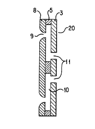
FIG. 2B, an entry orifice ll has a central axis XA extend-
ing in a first direction. The fluid ejection orifices 9
have central axes XB and XC parallel to, but offset from
entry orifice axis XA.
A fluid to be dispersed flows into the fluid
dispersant spray director 20 through the entry orifice ll
and into an intermediate channel lO. An internal surface
of the third patterned layer 8 interrupts the linear flow
of the fluid, forcing the fluid to undergo a turbulence
inducing angular fluid path transition prior to exiting
the intermediate channel lO and spraying through two fluid
ejection orifices 9. In the illustrated embodiment,
channel lO extends in a direction substantially perpendic-
ular to the orifice axes XA, XB and XC.
FIGS. 4A-4B depict another preferred embodiment of
a completed spray director 20. In this embodiment, there
are four each of the entry orifice ll, intermediate
ch~nnel 10 and the fluid ejection orifice 9. Each inter-
mediate channel lO has an egg-shaped cross-section.
Advantageously, a spray director prepared accord-
ing to the invention can have a range of cross-sectional
diameters and thicknesses. For example, the fluid ejec-
tion orifices of a spray director can have a minimum
cross-sectional dimension from about O.OlO mm to about
2.00 mm, preferably from about 0.020 mm to about 0.500 mm.
The dimensions of the fluid ejection orifice 9 are driven
by fluid flow requirements and vary widely depending on
the application and pressure drop requirement across the
spray director. These ~im~n.qions may be determined by one
of ordinary skill in the art without undue experimenta-
tion.
The dimensions of the photoresist on the substrate
and electroformed layers, and the electroforming time,
determine the dimensions of the spray director. The
multilayer thickness of the spray director should be about
O.lO0 mm to about l.500 mm. A preferred thickness ranges
from about 0.300 mm to about 0.900 mm. Variations from
CA 0220~801 1997-0~-21
W096/22460 PCT~S96/01619
these exemplary ranges may therefore readily be made by
those of skill in the art.
More than one entry orifice 11 can be provided in
each spray director 20. One fluid ejection orifice 9 can
be provided in each spray director 20. Alternatively, two
(as ~hown) or three or more fluld ejection sriflce~ 9 can
be provided in each spray director 20.
The number of patterned layers in a spray director
is not limited to three. More than three patterned layers
can be provided, for example, to facilitate the formation
of more intricate cavities, orifices, flow paths, and the
like. For example, additional layers may be provided to
facilitate the formation of grooves, fins or ribs on the
downstream wall of the intermediate channel, which struc-
tures further impact fluid turbulence.
The axes of the entry and ejection orifice need
not be parallel, and need not be perpendicular to the
intermediate channel, as long as sufficient turbulence is
generated in the fluid.
A plurality of spray directors may be simulta-
neously fabricated on a single substrate. To allow the
parts to be removed from the substrate as a continuous
sheet and to facilitate handling of the array, thin
coupling strips may be electroformed to affix the final
electroformed layer of each spray director pattern to at
least one other of the spray director patterns. The
distance between the spray directors in the array pattern
may vary widely, with the goal being to minimize the
space.
Spray directors prepared according to the present
invention can be employed in applications re~uiring spray
directors with precision orifices, such as the precise
metering of a fluid. Such uses include, but are not
limited to, fuel injector nozzles for use in internal
combustion engines, printing nozzles for thermal ink jet
printing, drop on demand printing and piezoelectric drive
printing, and spray applications, including epoxy sprays,
paint sprays, adhesive sprays, cosmetic sprays, household
CA 0220~801 1997-0~-21
W096/22460 PCT~S96/01619
or industrial cleaner sprays and solder paste sprays, or
any other applications in which fluid atomization and
spray pattern control are desired.
While the invention has been described in detail
and with reference to specific embodiments thereof, it
will be apparent to those of ordinary skill in the art
that various changes and modifications can be made therein
without departing from the spirit and scope thereof.
-