Note: Descriptions are shown in the official language in which they were submitted.
CA 0220~810 1997-0~-21
WO 97/12397 PCT/US96/16023
MT-'RQ~T~ .A~ C ASSEMBLIES T~T-Ul~T~ 7
Z-AXIS ~ U~ lV~i FII.MS
This invention relates to the assembly and packaging of micro-
electronic devices, including semiconductor circuit chips,
printed circuit boards, thin-film networks (TFN's), and multi-
chip circuit modules; and more particularly to novel means for
interconnecting such devices and modules, electrically and/or
thermally.
R ~ ~'R~R.olJND
The effort to provide more reliable, more cost-effective means
for interconnecting microelectronic devices has been underway
for at least thirty years. The need for such improvement has
become steadily greater because of the long-term trend toward
greater circuit density, and the consequent need to reduce the
size of bonding pads on a circuit chip, and to narrow the
spacing between pads.
Virtually all semiconductor devices are assembled with the use
of wire bonding to provide ohmic interconnections to the metal
pads on the circuit chip. Currently available wire bonders
require at least 6 mils spacing from the center of one pad to
the center of an adjacent pad. This limitation has blocked
further reductions in the size of a circuit chip, and further
increases in circuit density. This and other limitations of
wire bonding have been known for several decadesi and yet,
there is no apparent hope for a break-through in wire bonding
that would accommodate dramatic reductions in the size and
spacing of bonding pads.
Efforts to replace wire bonding have included the use of "high
density interconnect" structures, using synthetic resin films
CA 0220S810 1997-0~-21
WO97/12397 PCT~S96/16023
having metal patterns that extend along one surface of the
film and extend through via holes in the resin film for making
ohmic contact with underlying pads on a circuit chip. See for
example Gorczyca et al, U.S. 5,161,093. Such prior
configurations do not address the need to develop packaging
for chips having greater circuit density, nor the need for
interconnecting with smaller pads and closer pad spacing on
each chip; but instead are directed to multichip
interconnections, using chips of known design.
IBM and others have used solder bonding of inverted chips, as
an alternative to wire bondingi but no such soldering
technique has permitted the use of smaller pads and closer
spacing between pads.
More recently, elastomeric polymer films having multiple,
metal-
filled apertures have been developed for electrical
connections, but the metal filling has consisted of either
l) discrete particles ~usually spherical) or 2) a single
sphere having a diameter slightly greater than the thickness
of the polymer film, such that the sphere is barely exposed at
both surfaces of the film. The particle-filled films have not
been satisfactory, because the particle-to-particle surface
contact area within the film is extremely limited, causing
excessive electrical and thermal resistance at each contact
point; and because the surface contact area between a particle
and a bonding pad is also very limited. The sum of all these
high-resistance contact points gives the interconnection a
poor performance rating.
The single sphere approach is also unsatisfactory, because the
surface area of the contact point with the sphere, on each
side of the film, is too small; and because the film thic~ness
CA 0220~810 1997-0~-21
W097/12397 PCT~S96/16023
is fixed by the diameter of the spheres, and thus the film
cannot readily be deformed to accommodate the need for a non-
uniform thickness range. The use of deformable, gold-coated
polymer spheres randomly distributed within a polymeric
adhesive has been tried, but each gold-coated sphere had a
diameter about the same as the width of a single bonding pad,
which gave an unreliable result. Moreover, adjacent spheres
could not be kept apart, and there was no potential for
substantially reducing the space between bonding pads.
An elastomeric connector block comprising a plurality of
laminated silicone sheets, with parallel gold traces deposited
on the surface of each sheet, has provided electrical
connection between circuit boards having terminal pads with a
minimum width of 15 mils, which is far too large for
connecting pads on an integrated circuit chip.
No anisotropically conductive film has had the potential to
replace wire bonding, and to replace other means for the
interconnection of electronic parts, until now.
CA 0220~810 1997-0~-21
WO97/12397 PCT~S96/16023
SUMMARY OF THE l~v~..~lON
One aspect of the invention is embodied in an assembly of two
or more microelectronic parts, wherein electrical and/or
thermal interconnection between the parts is achieved by means
of multiple, discrete, conductive nanoscopic fibrils or
tubules fixed within the pores of an insulating film. The
pores are usually perpendicular, or substantially
perpendicular to the plane of the film, and extend through the
complete thickness of the film. Such a film is said to have
anisotropic electrical conductivity, i.e., Z-axis
conductivity, with little or no conductivity in the other
directions.
The insulating film of the assembly is selected from various
materials, including synthetic resin films, also known as
polymeric membranes. In addition to thermal and electrical
connection, such films are also capable of providing
structural connection between parts, for example, by
adhesively bonding the parts together, and thereby permanently
fixing the tips of the metal fibrils in contact with the
parts. Alternatively, the parts may be held together with a
non-bonding Z-axis film in between, by pressure alone, using
any suitable clamping mechanism. Such an alternative allows
the parts to be readily separated, for the purpose of
replacement or repair, etc.
A single integrated circuit chip having more than one thousand
bonding pads, for example, is now readily packaged, using the
interconnection system of the invention. Also, two or more
such circuit chips are readily interconnected with each other
in accordance with the invention. Or, one or more circuit
chips comprising active components may be mounted upon and
interconnected with ohmic contacts on a passive substrate.
CA 0220~810 1997-0~-21
WO97/12397 PCT~S96/16023
Instead of a passive substrate, one or more circuit chips may
be mounted upon and interconnected with ohmic contact pads on
a printed circuit board, or a microstrip line, or TFN, or a
package base. Such permutations and combinations are
virtually endless, all of which are included within the scope
of the invention.
One example of a suitable Z-axis conductive film useful in
accordance with the invention is a synthetic resin membrane
having nanometer-sized pores extending through the film, from
one membrane surface to the other surface, and having at least
some of its pores filled with a conductive material or
composition, such as gold or other metals, or with one or more
nonmetallic conductive materials. The thickness of the film
is within the range of about five microns, up to about l0
mils. The dimensions of the film and the metal fibrils ensure
good performance at 50 GHz and higher frequencies.
The nanoscopic pore diameter in such a membrane is much
smaller than the smallest spacing between contact pads on a
circuit chip; and therefore no electrical shorting between
adjacent contacts can be caused by such metal-filled pores,
regardless of chip orientation or alignment. For purposes of
this disclosure, the terms "nanoscopic", ~nanoporous~ and
"nanometer-sized" include diameters within the range of about
l nanometer, up to about l0,000 nanometers (l0 microns), and
preferably from l0 nanometers to l,000 nanometers (l micron).
CA 0220~810 1997-0~-21
WO97/12397 PCT~S96/16023
For example, on a chip having one thousand contact pads, a
suitable spacing between pad centers is about 0.5 mil, or
about 12.5 microns, which equals 12,500 nanometers. Thus, the
tip of a metal fibril fixed within a pore having a 10-
nanometer diameter covers or contacts only l/1250th of the
distance between pad centers. For pads having a width of 0.2
mil, and a center-to-center spacing of 0.3 mil, the space
between edges of adjacent pads is 0.1 mil, or 2,500
nanometers. Such a metal fibril tip would contact only
1/250th of the space between pad edges. A 100-nanometer
fibril tip would span only l/25th of the space between pads.
A distinguishing feature of the preferred nanoporous films
used in accordance with the invention is the aspect ratio of
the pores. That is, for a one-mil-thick film, each pore
length is one mil, or about 25,000 nanometers; and thus, for a
pore diameter of 10 nanometers, the aspect ratio is 2500:1.
The range of suitable aspect ratios for use in the invention
is from about
10:1 up to about 20,000:1, and preferably from about 100:1 to
about 1,000:1.
A further advantage of the invention lies in the fact
that precise alignment of the interconnect film with other
parts is not required, in order to achieve a desired ohmic
interconnection. Acceptable alignment is achieved when some
portion of each pad on a chip is aligned with some portion of
its counterpart on a substrate or other part to which bonding
is desired, provided no overlap with an adjacent pad is
allowed.
CA 0220~810 1997-0~-21
WO97/12397 PCT~S96/16023
For the dissipation of heat, thermal interconnection between
parts is achieved in the same manner as described above for
electrical interconnection, except that the nanopores are
filled with a material having high thermal conductivity.
Further, in order to maximize thermal conductivity, the number
and/or size of the pores is increased, so that a high
percentage of the membrane volume consists of the filled
pores. For example, a membrane consisting of 20% gold by
volume has a Z-axis conductivity approaching 60 W/M degree C.,
whereas a commercial adhesive, designed for heat dissipation,
has a thermal conductivity of
only 5 W/M degree C.
If electrical connection is not desired, in addition to heat
dissipation, the material in the pores is selected from
electrically nonconductive materials having a high thermal
conductivity, such as diamond, carbon, or boron nitride, for
example.
Nanoporous films of the type used in practicing the invention
are commercially available for use as nanofiltration
membranes. They are made, for example, by exposing a
nonporous resin film to accelerated nuclear particles having
sufficient energy to pass through the entire thickness of the
film, followed by selective chemical etching to remove the
particle-damaged tracks, and thereby create nanopores through
the complete thickness of the film. The etching step may also
remove small amounts of the surrounding undamaged film.
CA 0220~810 1997-0~-21
W097/12397 PCT~S96/16023
Such methods ha~ produced films having pores a. ;~a~ a1s l0
nanometers in diameter, and pore densities approaching l0 to
the ninth power pores per square centimeter. Polycarbonate
and polyester resin films having such pore specifications are
available from Nuclepore, Inc., and from Poretics Corp. One
example is the polycarbonate screen membrane from Poretics,
Catalog No. l9368PCTE.
Other methods for producing such nanoporous films include the
use of lasers, x-rays, gamma rays, or electron beams to burn
nanoscopic damage tracks and/or holes through a resin film.
Selective chemical etching is then used to create nanoscopic
pores, or to enlarge the holes in the film. The pores are
then filled with a metal or other conductor by electroplating,
electroless plating, or vapor deposition. Excess metal
formed on the membrane surface or surfaces is then removed,
whereby the only remaining metal is located in the pores.
If desired, the membrane is then exposed to an etchant that
does not attack the metal, so that a small amount of the
membrane surface surrounding the tips of the metal fibrils is
removed, thereby providing tips that extend slightly above the
remaining membrane surface. The exposed tips may then be
tinned with solder, to achieve solder contact with the pads of
a circuit chip or substrate, etc., . desired. It has been
demonstrated, however, that reliable electrical
interconnection is achieved by contact alone, without solder
bonding or any other form of fixed attachment to the tips of
the metal nanofibrils used in accordance with the invention.
Methods for plating and filling the inside of such nanopores
have been developed by Dr. Charles R. Martin et al, as
reported in the following articles:
CA 0220~810 1997-0~-21
WO97/12397 PCT~S96/16023
"Nanomaterials: A Membrane-Based Synthetic
Approach,"
Science, Vol 266, pages 1961-6, Dec. 23, 1994
"Template Synthesis of Metal Microtubule Ensembles
~ Utilizing Chemical, Electrochemical, and Vacuum
Deposition Techniques," J. Mater. Res., Vol 9,
No. 5, Pages 1174-83, May 1994
"Fabrication and Evaluation of Nanoelectrode
Ensembles"
Analytical Chemistry, April 15, 1995
"Metal Nanotubule Membranes With Electrochemically
Switchable Ion-Transport Selectivity", Science,
Vol 268, May 5, 1995
"Preparation and Electrochemical Characterization of
Ultramicroelectrode Ensembles," Analytical
Chemistry,
Vol 59, No. 21, Pages 2625-30, Nov 1, 1987
Each of the above-cited articles is incorporated herein by
reference. A copy of each article is included herewith.
The use of single nuclear particle guns, lasers, x-rays or
electron beams to generate the damage tracks or holes allows
convenient patterning of the pore locations. For example, the
pores may be arranged in a rectangular or triangular pattern;
and moreover, selected surface areas without pores may be
provided, so that conductive thin film patterns may be
fabricated on such surface areas of the membrane, for current
propagation in x-y directions, combined with z-axis conduction
in other areas of the same membrane. The same result can be
CA 0220~810 1997-0~-21
PCT~S96/16023
WO97tl2397
achieved, beginning with a random distribution of pores, by
selectively masking portions of the membrane surface during
etching or plating.
Polymeric membranes used in accordance with the invention
include both thermoplastic and thermosetting polymer films.
For example, upon heating the combination of an electronic
device in contact with a metal-filled, nanoporous
thermoplastic membrane, the softening of the plastic causes an
adhesive bonding of the device to the membrane, thereby
holding the tips of the metal fibrils in contact with the
device.
A thermosetting polymeric membrane having metal-filled pores
is also useful for the same purpose, except that the heating
step causes a permanent hardening (cure) of the film, thereby
bonding the devices to the surface of the membrane, and
holding the fibril tips in place.
For certain applications, an elastomeric film composition is
preferred. The surface of such a film will conform completely
with the microscopic irregularities of a circuit surface, and
thereby permit maximum contact area between each film surface
and each circuit or substrate surface. Such a film interface
also causes virtually all the metal fibril tips to make good
contact with the circuit surface, including each bonding pad,
on both sides of the film. The net result is a very low
resistance interconnection.
For example, in a membrane having a high pore density, the
filled pores represent more than 20% of the composite film
volume. Thus, at least 20% of each bonding pad area is
contacted with metal, which ensures a very low resistance
connection.
CA 0220~810 1997-0~-21
WO97/12397 PCT~S96/16023
Also, a pressure-sensitive adhesive surface can be prepared by
using a pressure-sensitive adhesive film, or by coating the
membrane with a tackifier, such as silicone polymer. Such a
tacky surface holds circuit chips in place on the surface of
the membrane.
The Z-axis conductive films of the invention have the
additional advantage of enabling a reliable interconnection of
parts that are not perfectly planar. That is, all the contact
pads on a device surface are normally designed to lie in
precisely the same plane. But if one or more of the pads
deviate from the plane, defective or unreliable bonding can
result. Now, such nonplanar pads can be reliably bonded,
since the films of the invention exhibit a sufficient plastic
"flow" to engage all such pads.
When the film is thus deformed, some deformation of the metal
fibrils also occurs. Because of the high aspect ratio of the
metal fibrils, such deformation introduces no adverse effect.
In order to further enhance membrane flow, a large number of
pores may be kept open, i.e., unfilled. This allows the film
to exhibit compressibility, which is not characteristic of a
normal polymeric film.
Still further, by careful selection of the composition of the
polymer, the x-y and/or z coefficient of thermal expansion
(CTE) for the membrane can be approximately matched with the
CTE of the parts bonded thereto. More specifically, the CTE
can be matched with that of silicon, metals and ceramics, such
as used in the fabrication of microelectronic semiconductor
devices, to provide improved reliability. Liquid crystal
polymers and rigid rod polymers are particularly suited for
this purpose, including Vectra from Hoechst, xyDAR from AMOCO,
CA 02205810 1997-05-21
W O 97/12397 PCTAJS96/16023
Poly X from Max Dern, PIBO from Dow, and certain polyimides
from DuPont.
12
CA 022058l0 l997-05-2l
WO97/12397 PCT~S96/16023
The following polymer compositions are among those suita~le for use
in accordance with the invention:
T9~RMOPLASTlC FSL~S FOR ~._ _ ~CTS
Pla-tic Tg C5~ Tm Lo-s %R70 C - ~
Vec~ra LC~ Hoecnst FA- 160 -5eo~~ 285C .002 .02 Pro~uc~lon PWB
X100-30 and bond fllm
Polypnenviene ~.ax~em l~Q 5eo ~5 .~05 .25 Pilot Plant
DuPont LCP 200 Pilot Plant
:~YDAR LCP (AMOCO~ 25~ ~ to4~ 320 .1
PolycarDonate 150 67 160 .006 .35 Present Film
(GE, '.~obav)
Polysuifone (AMOCO)15G .0C4
~'Thermaiuxl~ Cilm
x~ruded bv Westlake
E.~ ~ICI) _~4 334 Verv ~-ystalilne
o_vester T .. 3~ 30 .08
o.vester _T ~'
E_ 'lltem _JOO (GE) ,00 ~ 250 .~2 ._~
~x~ruded bv Westlake
r~ _vac v_a~e -.oecnst ~-
- Dlscor.t1nuea
~ ( u ont) 1 ~ . --
_ (B S-.A~OCO! _,C ~0
o_y~etone ~- J Very~ow aheli,Mod
Plas.Mar
L ~ ~ C ~st~i6_ 373
. (Ar C
. ~E ~ -! 17~ 3,1
(~M~_ 2~
__ cone pressure 260
sensltive Film,
Speclalty Tapes C~-14HT
~r CM-1050
T~CRMOSET BOAADS AND BOND FS~MS
~la-t~ ~g C~E Tm Lo-s ~,0 C~ ~ E
~400Q BDN STYRENE 290 ., 0'~ .06 PWB
.ogers & .I Bond flim ~ Film
e available soon
olvlmlde DuPont P'2610D 400 3 .0C2 .6 Sp n on
IBO (Dow) >400 ' Fi.m, spln
~peeaDoard Adheslves C- tagea AdAeslve
(Gore) Film
8R~EF n~r~~ . OF 1~5 DRA~INaS
Figure 1 is a greatly enlarged cross-sectional view of a prior
anisotropically conductive microelectronic connection, using
a polymeric adhesive film having 40-micron metal spheres
distributed therein.
CA 02205810 1997-0~-21
WO97/12397 PCT~S96/16023
Figure 2 is a greatly enlarged cross-sectional view of a
micro- electronic connection interface in accordance with the
invention, using a microporous polymeric Z-axis conductive
film having a 5-micron diameter gold fibril fixed within each
film pore.
Figure 3 is a greatly enlarged cross-sectional view of a
micro- electronic connection interface in accordance with the
invention, using a nanoporous polymeric Z-axis conductive film
having a 0.375-micron diameter gold fibril fixed within each
film pore.
Figure 4 is a greatly enlarged cross-sectional view of a
micro-
electronic connection interface in accordance with the
invention, using a nanoporous polymeric Z-axis film having a
25-nanometer diameter gold fibril fixed within each pore.
Figure 5 is a greatly enlarged cross-sectional view of plural
microelectronic interconnections in accordance with the
present invention, using a nanoporous polymeric Z-axis film
having a 25-nanometer gold fibril within each pore.
Figure 6 is a cross-sectional view of a nanoporous resin film
having some orthogonal pores filled with gold fibrils.
Figure 7 is a cross-sectional view of a nanoporous resin film
having oblique and orthogonal pores filled with gold fibrils.
Figure 8 is a cross-sectional view of a nanoporous resin film
having selected pores filled with gold, and other pores filled
with a thermally-conductive dielectric material.
CA 0220~810 1997-0~-21
W097/12397 PCT~S96/16023
Figure 9 is a top view of a package base and an integrated
circuit chip to be mounted therein according to the invention.
Figure 10 is a cross-sectional view of two circuit chips,
inter-
connected with each other in accordance with the invention.
Figure 11 is a cross-sectional expanded view of an assembly
comprising a plurality of printed circuit boards
interconnected with the Z-axis film of the invention.
Figure 12 is a perspective view of a Z-axis conductive film,
used
to form interconnections in accordance with the invention.
Figure 13 is a perspective view of a conceptual composite of a
Z-axis conductive film, useful in accordance with the
invention, showing numerous pore variations and combinations.
CA 0220~8l0 l997-0~-2l
W097/12397 PCT~S96/16023
D]5T~TT.~n 11~-5~'~TPTION
As shown in Figure 1, the prior use of 40-micron metal spheres
11 within a polymeric adhesive film is unsatisfactory, because
the sphere provides a very small surface contact area with
bonding pads 12 and 13. Although the pads have polished
surfaces, nanoscopic irregularities remain, making it more
difficult for spheres 11 to achieve good contact. Because the
contact area is very small, low-resistance contact is
impossible. Even the use of three or more spheres per pad
will not correct this problem. A contact pad is not large
enough to permit contact with more than three or four such
spheres. Moreover, the spheres do not enable adequate
tolerance or adjustment to the bonding of nonplanar surfaces.
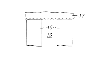
As shown in Figure 2, one embodiment of the present invention
includes the use of 5-micron diameter metal fibrils 15 within
each pore of film 16, such that multiple fibril tips make
contact with pad 17. Although a single fibril tip may not
provide substantially more surface contact area with the pad
than sphere 11, the key difference is that 230 fibril tips
will fit within the same pad area that accommodates only three
of the spheres. Thus, the total resistance of the contact in
Figure 2 is substantially less than the total resistance of
the contact in Figure 1; and may be only 1/50th or 1/lOOth as
great.
As shown in Figure 3, another embodiment of the invention
includes the use of 0.375-micron diameter metal fibrils 21
within the pores of film 22, for making electrical contact
with pad 23. Even though each fibril may contact only a single
point on pad 23, the number of fibril tips that contact a
single pad exceeds 40,000. Thus, the total resistance of the
16
CA 0220~810 1997-0~-21
WO97/1~97 PCT~S96/16023
contact in Figure 2 is much greater that the total resistance
of the contact in Figure 3.
As shown in Figure 4, nanoscopic metal fibrils 26 within
polymer film 27 have a diameter of ony 25 nanometers, such
that the tips are readily capable of entering each of valleys
27 in the surface of pad 28. This intimate contact, in
combination with the
large number of fibrils that contact each pad, provides an
even lower resistance contact than the embodiment of Figure 3,
and is comparable with the resistance characteristic of an
alloyed wire bond. Still further, the dynamic thickness range
of the film is greater, due to the greater aspect ratio of the
film pores, and the greater degree of deformability of the
metal fibrils in the pores. Actual contact resistance is a
function of a number of parameters, including fibril
deflection force, malleability of the metal, surface
roughness, planarity of the parts, and others.
As shown in Figure 5, the film used in accordance with the
invention is capable of deforming under pressure to fill the
entire space between circuit parts. Consequently, nanoscopic
fibrils 31 readily deform, as a result of film compression
between pads 32 and 33. Similarly, fibrils 34 readily deform,
as a result of film compression between pads 35 and 36. The
remaining fibrils 37 are not compressed, and they make no
electrical contact, but they do serve to conduct heat.
As shown in Figure 6, an example of the interconnection means
of the invention comprises synthetic polycarbonate resin
membrane 41 having a thickness of 1 mil, and up to one million
or more parallel nanoscopic pores 42, each pore having a
diameter of about 30 nm, at least some of which are filled
with gold nanofibrils 43. Many other membrane compositions
CA 0220~810 1997-0~-21
WO97/12397 PCT~S96/16023
are useful in accordance with the invention, as well as many
other dimensional specifications. For electrical
conductivity, the gold may be replaced with another metal or
other conductive material, including copper, platinum, nickel,
and silver, for example. Conductive polymers are also useful
nanofibrils for some applications, including polyacetylene,
polypyrrole, polythiophene, and polyaniline, for example.
Polysilicone membranes are particularly useful in that they
have
a low elastic modulus which allows the film to accommodate the
deflections or deformations associated with the bonding of
contact pads on nonplanar surfaces; and also allows greater
tolerance to the interconnection of parts having different
coefficients of thermal expansion.
As shown in Figure 7, another example of the interconnection
means of the invention comprises synthetic polyester membrane
44 having a thickness of 1 mil, a first multiplicity of
parallel nanoscopic pores 45 orthogonal to the membrane
surface, a
second multiplicity of parallel nanoscopic pores 46 sloped at
a substantial angle with respect to pores 4~, and preferably
a third multiplicity of nanoscopic pores 47, sloped at a
substantial angle with respect to both pores 45 and 46. Pores
15 are filled with gold, for example, for the purpose of
electrical conduction, while the other pores are filled with a
material having greater thermal conductivity than gold, but
electrically nonconductive, such as diamond, for example, so
that greater heat dissipation is achieved, especially in the
x-y directions, compared with the example of Figure 1.
As shown in Figure 8, another variation of the interconnection
membrane comprises synthetic resin film 48 having pores 49
CA 0220~810 1997-0~-21
WO97/12397 PCT~S96/16023
filled with gold, pores 50 filled with a material having
greater thermal conductivity than gold, and pores 51 left
open, for the purpose of allowing the membrane to exhibit
compressibility, and a lower apparent modulus of elasticity
than is characteristic of a nonporous membrane having the same
composition.
As shown in Figure 9, a single circuit chip 52 is inverted
within package base 53 such that contact pads on the face of
the chip are electrically interconnected with pads 54 of base
53, by means of membrane 41, separately illustrated in Figure
1. No alignment of membrane 41 is required, except to cover
all of pads 54, since all portions thereof include gold-filled
pores. Approximate alignment of the chip is required, only to
ensure that some portion of each contact pad is vertically
oriented over some portion of the corresponding pad on base
53. The chip is held in place by the top of the package, (not
shown) which is designed to apply pressure to the chip, when
the package is fully assembled. Or, membrane 41 is selected to
function as an adhesive by itself, with or without first
applying heat to soften the membrane surface, so that a
permanent chemical bonding of the membrane to both the chip
and the package base occurs.
As shown in Figure 10, two circuit chips 61 and 62 are readily
interconnected by means of nanoporous anisotropically
conductive membrane 63 having at least some of its pores
filled with gold or other conductor. The chips are
interconnected with substrate 64 by means of nanoporous
anisotropically conductive membrane 65.
As shown in Figure 11, a plurality of circuit boards 71 having
contact pads 72 are readily interconnected by means of Z-axis
conductive films 73 and 74, respectively.
19
CA 0220~810 1997-0~-21
WO97/12397 PCT~S96/16023
As shown in Figure 12, Z-axis film 81 includes a large number
of metal-filled pores 82, a large number of unfilled pores 83,
and a substantial area 84 without pores, achieved by masking
the area during the pore-forming procedure.
As shown in Figure 13, Z-axis conductive film 91 includes a
variety of pore configurations, and a variety of pore
contents.
Specifically, film 91 includes an area of random pore
distribution, a rectangular grid array of metal-filled pores,
a triangular grid array of metal-filled pores, a square
pattern of semiconductor-filled pores, a number of unfilled
pores, and a number of partially-filled pores, illustrating
conceptually that a multiplicity of combinations and
permutations are within the scope of the invention.