Note: Descriptions are shown in the official language in which they were submitted.
CA 02206018 1997-0~-16
WO 96/16344 PCT/AU95/00766
lNVU~;lN~ OR EN~ANCING ELECTRO-OPTIrZ~- PRO~ ; IN
OPTICAI.I.Y T~ANSMISSIVE ~ATERIAL.
Field of the Invention
This invention relates to a process for inducing or
enhancing electro-optic properties in optically
transmissive material and to optical devices comprising
or incorporating material that has been subjected to such
process. More particularly but not exclusively, the
present invention relates to a process for producing an
optically transmissive material having electro-optic
properties for use in an optical waveguide such as an
optical fibre.
Backaround of the Invention
Electro-optic materials, i.e. materials whose
refractive index (RI) varies with application of an
electric field currently are known, an example of such a
material being Lithium Niobate (LiNbO3). The existence
of the electro-optic property provides for the
development of various optical/light transmitting devices
whose RI may be controlled by the application of an
electric field.
Lithium Niobate waveguide modulators are
commercially available but there are limitations inherent
in relation to the existing technology. Fabrication of
devices employing Lithium Niobate is complex and the
materials are expensive. Its high dielectric constant is
not entirely appropriate for the realisation of high
speed, low voltage devices and the differences between
Lithium Niobate and silica optical fibre both in terms of
linear refractive index and of waveguide geometry make
low loss coupling to standard fibre systems difficult.
Furthermore, at short (e.g. blue) wavelengths lithium
niobate suffers from photorefractive damage.
By far the most practical and readily available
material for optical devices is silica or silicate glass
~referred to herein for convenience as "silica glass" or
nglass~), but unfortunately, silica glass displays little
or no electro-optic properties.
An attempt has been made to enhance electro-optic
properties in doped silica glass devices by heating the
SUBSTITUTE SHEET (RULE 26)
CA 02206018 1997-0~-16
WO96116344 PCT/AU95t00766
devices in the presence of an applied electric field.
This has had some effect but the resultant electro-optic
effect has proved to be insufficient for practical
purposes.
Attempts have also been made at enhancing the
electro-optic properties of doped silica glass utilising
visible light in the presence of an applied electric
field. "Generation of Permanent Optically Induced
Second-Order Nonlinearities in Optical Fibers by Poling~
by Bergot et al appearing in Optics Letters, Volume 13,
No. 7, July 1988 at pages 592-594 (Bergot et al)
discusses a process of inducing a second order optical
nonlinearity in germanosilicate fibres by applying a
transverse DC electric poling field in the presence of a
high intensity light. Bergot et al discloses utilising a
pulsed laser operating at 485nm and a CW argon laser
operating at 488nm. It further discloses launching light
from these lasers axially into the core of the fibre in
the presence of a DC electric field. This has had some
effect but again, the resultant electro-optic effect has
proved insufficient for practical purposes.
Summary of the Invention
In contrast, in the present invention, it has been
found that, by utilisation of electromagnetic radiation
of higher frequencies, for example, ultra violet (W)
substantially improved results are obtained. Further,
Bergot et al in utilising lower frequency visible light,
allows for the light to be launched axially into the
fibre. However, electromagnetic radiation in the W
portion of the spectrum is highly absorbed in silica
glass. However, by launching the light transversally
into the fibre, the W light can be caused to have effect
in producing an optically transmissive material having
enhanced electro-optic properties.
Therefore, the present invention provides a process
for inducing or enhancing electro-optic properties in an
optically transmissive material and which comprises
applying an electric field to the optically transmissive
CA 02206018 1997-0~-16
WO96/16344 PCT/AU95/00766
material and subjecting the material to incident
electromagnetic radiation in the ultra violet portion of
the spectrum.
The present invention further provides an optical
device which comprises or includes an optically
transmissive material which has been subjected to the
above defined process.
The intensity or phase of the W electromagnetic
radiation may be varied either in time or spatially along
the device to produce a non-uniform enhanced electro-
optic response. Also or alternatively the electric field
may be varied either spatially or in time.
The material subjected to this process would
normally comprise silica glass and, in a preferred
embodiment, the process may be applied directly to a
silica glass optical fibre. The wavelength of the
electromagnetic radiation used in irradiating an optical
fibre must be such that, when irradiated in a transverse
direction through the cladding, the cladding of the
optical fibre will not totally absorb the radiation, so
that the radiation will penetrate, and be substantially
absorbed in, the core region of the fibre.
In the preferred embodiment, the electromagnetic
radiation is selected such that it interacts strongly
with the core of the silica glass optical fibre.
Alternatively, the radiation can be selected so that it
interacts strongly with the core and a portion of the
cladding glass that the propagating mode will extend
into. In order for a strong interaction to take place,
the electromagnetic radiation must be absorbed. The
absorption edge of silica is deep in the W (around
160nm). However, the presence of defects in the silica
glass, especially due to doping in the core, results in
absorption bands at longer wavelengths. For instance, in
germanosilicate optical fibres, strong absorption bands
are found at approximately 193nm and 240nm.
Electromagnetic radiation at these wavelengths will be
absorbed significantly. Typically, half the power of the
CA 02206018 1997-0~-16
W O96/16344 PCT/AU95/00766
-- 4
radiation will be absorbed within a few tens or hundreds
of wavelengths which is in the order of a typical single
mode fibre core diameter. At longer wavelengths, such as
that utilised in Bergot et al, the electromagnetic
radiation has only a weak interaction with the optical
fibre core as the wavelength is spectrally remote from
any absorption peak, with the resulting absorption being
approximately one million times smaller. Further, when
using radiation at a wavelength remote from an absorption
peak, light will generally have to propagate a
substantial distance along a fibre to create any useful
induced effect and that utilising transverse projected
radiation through the side of an optical fibre is not
practical because of the low level of absorption as the
light transverses the core whose ~-men~ions will be small
compared with the absorption length. Therefore,
radiation wavelengths as illustrated in Bergot et al
produce an impractically small electro-optic effect.
In a preferred embodiment of the process as applied
to an optical fibre, the radiation can be selected to lie
between 150nm and 400nm and, preferably, to lie in the
range 150nm to 350nm. The important factor is that the
radiation wavelength used must be capable of
significantly inducing or enhancing the required electro-
optic effect when the optical fibre is exposed to theelectric field. Expressed in more general terms, the
wavelength and the energy of the incident ultra violet
electromagnetic radiation can be determined by the glass
composition and the type and concentration of dopant(s)
within the glass.
The dopant species for inclusion in the silica glass
can be selected for optimum enhancement of the electro-
optic effect. The range of the preferred dopant(s)
includes those commo~ly used in the manufacture of
optical fibre. Such dopant compounds include those
capable of being converted to at least one metal oxide
selected from groups IA to VA, IB to IVB and the
trànsition metals, rare earths and actinides.
CA 02206018 1997-0~-16
WO96/16~ PCT/AU95/00766
Furthermore, P2O5 is commonly used as a dopant. Typically
dopants to be incorporated may be germanium, aluminium,
boron and/or rare earths (or lanthanides) such as erbium.
Hydrogen is also known to increase the sensitivity of
silica and/or silicate glass to electromagnetic radiation
and may be introduced by storing the structure in a high
pressure hydrogen atmosphere. Other dopants that can be
utilised are H2O and hydroxide ions.
The electric field preferably is applied across at
least a part of the region of the material to be exposed
to radiation in a direction transverse to the intended
direction of propagation of light through the material.
Field strengths of around 100 V/~m may be applied. In
the preferred embodiment, as applied to a silica glass
fibre, it is possible that field strengths greater than
100 V/~m may cause dielectric breakdown of the silica but
it is possible that much higher field strengths may be
applied. In general, a preferred field strength range is
1 V/~m to 1000 V/~m, and more preferably, in particular
as applied to a silica glass optical fibre, between 10
V/~m and 150 V/~m.
In one embodiment of the present invention, as
applied to an optical fibre, the application of such high
field strengths is facilitated by including electrodes
within the optical fibre cladding alongside the doped
silica glass core. It has been found in practice that it
is preferable to maintain the anode electrode as close as
possible to the core of the optical fibre. This appears
to give improved poling results.
The provision of electrodes in proximity to the
fibre core also facilitates subsequent application of the
treated fibre as an electro optic device, the electrodes
facilitating application of an electric field to control
light transmitting properties of the fibre.
optical fibre with electrodes embedded in the
cladding running close and parallel to the core may be
fabricated by:
(i)Drawing fibre with holes running parallel, close
CA 02206018 1997-0~-16
W O 96/16344 PC~r/AU9SI00766
-- 6
and placed diametrically across the core and
then inserting fine wires (or other conductors
or conducting materials);
(ii) Drawing fibre from a preform with electrodes
already in holes running parallel, close and
placed diametrically across the core, where the
electrode material typically has thermal
properties sufficiently close to that of silica
to allow both materials to be drawn
simultaneously.
In some instances it may be advantageous to have the
electrodes non-parallel (with respect to each other
and/or the core) and/or the axes of the electrodes may be
contained in a plane which is displaced with respect to
any plane containing the axis of the core. Furthermore
in some applications of the invention more than two
electrodes may be employed. There are many applications
where multi-core fibre would benefit from thi~ processing
technique. It is also preferable that at least one
electrode, preferably the anode, is in contact or near
contact with the core of the optical fibre. It should be
noted that the electrodes may or may not be used as
modulating electrodes in a final device. In some
applications they may only be present for the sole
purpose of applying the poling electric field. A simple
example of such an application is utilising the induced
electro-optic behaviour for its optical non-linear
properties in the area of second h~rmon;c generation.
Further, such use will also apply to other optical non-
linearities and to quasi-phase matched second harmonic
generation in a periodically poled device.
The present invention can also be readily extended
to a planar waveguide structure. Application of higher
field strength can take place via buried electrodes.
Alternatively, high field strength poling may be possible
with exposed electrodes. In this case, it may be
- necessary to apply the electric field in vacuum or with a
high pressure gas ~for example SF6) to avoid electrical
CA 02206018 1997-0~-16
WO96/16~ PCT/AU95/00766
-- 7
breakdown of the atmosphere. It may also be necessary to
treat the surface with a modifier layer to avoid tracking
across the surface. A modified atmosphere can also be
useful for further enhancement in the processing of the
optical fibre embodiment.
Preferably, the electromagnetic radiation and
electrical fields are applied simultaneously.
Alternatively, it is possible that pulsed electromagnetic
radiation and pulsed electric field could be used to
induce the electro-optic effect. The pulses of the
electromagnetic radiation and electric field may be
alternated.
The non-linearity obviously allows an electric field
to modify the refractive index of a material. Of course,
light itself consists of oscillating electric and
magnetic fields. The intrinsic electric field of light
can thus also act through the non-linearity to modify the
refractive index. This allows for the generation of
higher optical h~rmo~;cs of the light and mixing of light
of different frequencies to produce sum and difference
frequencies.
A variation on the process enables the production of
devices with predetermined tailored electro-optic
properties. In one variation, the incident
electromagnetic radiation can be varied, for example by
variation of the beam position, power, spatial
distribution or pulse rate to "write" a specifically
tailored structure to produce a desired optical device.
Alternatively or additionally, the applied electric field
can be varied to produce the desired device properties.
Such "tailored" devices can have any number of
applications, depending upon the properties incorporated.
The present invention may be applied to materials
other than silica or silicate glasses. Other possible
optically transmissive materials include fluorozirconate
or chalcogenide glasses and optically transmissive
plastic material. Different wavelengths and perhaps
different dopants may be required.
CA 02206018 1997-0~-16
Wo96/16~ PCT/AUgS/00766
-- 8
The invention may be realised in various practical
embodiments and be applied to various light transmitting
devices, including optical fibres and planar waveguides.
Brief Description of the Drawings
Features and advantages of the present invention
will become apparent from the following description of an
em~bodiment thereof in optical fibre form, by way of
example only, with reference to the accompanying
drawings.
In the drawings:
Figure 1 is an end view of an optical fibre adapted
for processing in accordance with an embodiment of the
present invention;
Figure 2 is a side view of the optical fibre of
Figure 1, having electrodes inserted within the optical
fibre cladding; and
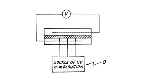
Figure 3 shows a method of applying the ultra violet
electromagnetic radiation to the core of an optical
fibre.
Description of the Preferred Embodiments
With reference to the drawings, an optical fibre,
generally designated by reference numeral 1, comprises a
doped silica glass core 2, surrounded by a cladding 3 of
silica or doped silica glass. The silica glass core 2
was doped (prior to drawing out the fibre 1). Dopants
used in this example were concentrations of 12 mol~ Ge,
3 mol~ Al and 35Oppm of Er.
The optical fibre 1 was drawn out with a pair of
hollow channels 4 bracketing the optical fibre 2.
Fine wire electrodes 5, 6 (Figure 2), in the order
of 3-4cm long were inserted in the channels 4 so that
they lay alongside the core 2 slightly spaced therefrom.
The ~lmen~ions specified in the drawings being exemplary
only.
The electrodes S and 6 were excited by the
application of an electrical poling field at a strength
of approxim.ately 80 V/~m while radiation of a wavelength
of 193nm at a power of 35 mJ/cm2 was focused transversely
CA 02206018 1997-0~-16
WO96/16~ PCTIAU95/00766
g
onto the fibre core at a rate of lOpps (pulse per
second), from a pulsed laser source 9, for around 10
minutes.
This treatment produced a significant apparently
linear electro-optic coefficient of around 6 pm/V in the
doped silica glass, far more significant than that
reported by Bergot et al.
The application of the ultra violet electromagnetic
radiation and the electric field may be varied to create
numerous types of devices with pre-determined properties.
Further, the presence of electrodes adjacent the fibre
optic core enables their subsequent use in the
application of a modulating electric field.
Figure 3 shows the preferred method of applying the
W electromagnetic radiation to a core of an optical
fibre in a direction transverse to the direction of
propagation of light through the optical fibre.
In a second embodiment, a poled Bragg grating having
a periodic structure was created. A fibre was
constructed in accordance with Fig. 1 however, this time
the fibre had an outside diameter of 300 ~m. The
diameter of hollow ch~nnels 4 was 70 ~m with the two
hollow channels 4 being separated by 18 ~m and a central
core 2 having an 8 ~m diameter being located between the
two hollow channels 4. Two electrodes, having diameters
50 ~m were inserted into the optical fibre having a
length of approximately 6 cm. A voltage was applied
between the electrodes so as to set up an electric field
strength of approximately 100 V/~m.
The structure wa~ then irradiated at 240nm from an
excimer pumped frequency doubled dye laser for about 1
hour at 0.8 mJ (25 mJ/cm2) and at 20 Hz. The laser
irradiation was passed through a phase mask (not shown)
so as to create a periodic pattern of irradiation
corresponding to a Bragg grating structure having an in
fibre reflection wavelength in the region of 1.53 ~m.
The resulting tunable Bragg grating reflector was
modulated by applying up to +/-300 V to the electrodes
CA 02206018 1997-0~-16
W O 96/16344 PCT/AU95/00766
- 10 - .
and Reflectivity changes of approximately 15 dB and Bragg
wavelength shifts of approximately 0.5nm were observed.
These observations being consistent with an induced
electro-optic coefficient of approximately 1 pm/V in the
nom1n~lly unexposed regions and approximately 10 pm/V in
the exposed regions.
The foregoing description of the preferred
embodiments is by way of illustration only.
Modifications, obvious to those skilled in the art can be
made thereto without departing from the scope of the
invention.