Note: Descriptions are shown in the official language in which they were submitted.
CA 02206037 2001-02-07
'\\
SUBSTITUTE SPECIFICATION
PLANAR FILTER WITH FERROELECTRIC AND/OR
ANTIFERROELECTRIC ELEMENTS
CA 02206037 2001-02-07
BACKGROUND OF THE INVENTION
The present invention relates to a planar filter with ferroelectric
and/or antiferroelectric elements.
Such a planar filter with ferroelectric and/or antiferroelectric
elements is disclosed for example in the patent document WO 94/28592. In
this filter a ferroelectric or antiferroelectric layer is mounted on a
dielectric
substrate. The microstructured high temperature super-conductive layer is
arranged on the layer substrate and in particular on its upper side, while an
unstructured high temperature super conductive layer is also arranged on the
lower side. Together they form a filter in the microstrip conductor form. A
planar electrode is located several millimeters above the upper
superconductive structure. By applying a voltage between the upper high
temperature superconductive layer and the planar electrode, the effective
dielectric constant of the intermediate space between the structure
superconductive layer and the unstructured super-conductive layer can be
changed since the dielectric constant of the ferroelectric or the
antiferroelectric substantially varies in dependence on the applied voltage.
Thereby the filter characteristic also changes, in particular its transmission
frequency.
-2-
CA 02206037 2001-02-07
SUMMARY OF THE INVENTION
Accordingly, it is an object of present invention to provide a
filter of the above mentioned general type, which has particularly low losses.
In keeping with these objects and with others which will
become apparent hereinafter, one feature of present invention resides,
briefly stated, in a planar filter of the above mentioned type, which has a
wave guide arranged on an upper side of a substrate, and at least one tuning
element composed of ferroelectric andlor antiferroelectric material with which
a voltage applied to the ferroelectric or antiferroelectric element and
thereby
the dielectric constant can be adjusted, wherein the tuning element is
arranged at an upper side of a substrate.
By the arrangement of the ferroelectric or antiferroelectric
tuning element above the superconductive microstructure, a substrate with
optimal dielectric properties can be selected between both superconductive
layers. Moreover, it is especially advantageous that with the selection of the
substrate the requirements of the epitactic growth of the superconductive
layers on the dielectric substrate can be particularly taken into account. As
a result, with better producable superconductive layers, high grade ~ilters
are
realized.
-3-
CA 02206037 2001-02-07
In accordance with another feature of present invention, it is
especially advantageous when the filter element and the tuning element are
separate components. Thereby coarse tuning can be performed by selection
of a corresponding ferroelectric or antiferroelectric tuning, while fine
tuning
can be performed electrically on the assembled components.
Moreover, it is advantageous when the conductor layers are
produced from superconductive cuprates. Thereby the cooling of the filter
can be performed less expensively than with the use of conventional
superconductors.
Furthermore, it is especially advantageous when the
ferroelectric or antiferroelectric element is produced from a layer applied on
the housing cover. Thereby a very simple mechanical mounting and low
expense during adjustment are provided.
It is also especially advantageous when the ferroelectric or
antiferroelectric element is produced from a layer which is mounted on the
planar filter substrate with insulating spacers. Thereby the filter remains
adjustable also with removed cover.
It is also advantageous when the ferroelectric or
antiferroelectric layer is subdivided by microstructuring methods into
-4-
CA 02206037 2001-02-07
individual segments. Thereby the dielectric constants of each individual
element can be regulated separately, since therefore a band path filter
element is produced with upper and lower edges and its fine structure is
finally adjustable separately within the transmission band.
Further, it is especially advantageous to use several massive
ferroelectric or antiferroelectric bodies as the tuning elements. Thereby the
tuning region for each individual resonator element of the planar filter is
expanded.
Finally it is especially advantageous when the individual
ferroelectric or antiferroelectric tuning elements are provided with a
displacing device. Thereby a wider regulating and compensating region can
be obtained.
The novel features which are considered as characteristic for
the present invention are set forth in particular in the appended claims. The
invention itself, however, both as to its construction and its method of
operation, together with additional objects and advantages thereof, will be
best understood from the following description of specific embodiments when
read in connection with the accompanying drawings.
-5-
CA 02206037 2001-02-07
BRIEF DESCRIPTION OF THE DRAWINGS
Figure 1 is a view showing a planar filter in accordance with the
present invention with microstrip conductor structure and with a planar
ferroelectric tuning element arranged above it;
Figure 2 is a view showing a filter in coplanar construction with
a microstructured tuning element located above and composed of several
ferroelectric or antiferroelectric tuning elements; and
Figure 3 is a view showing a planar filter with a microstrip
conductor structu re with massive ferroelectric or antiferroelectric
interference
bodies for tuning which are movably suspended on a housing wall by screws.
-6-
CA 02206037 2001-02-07
DESCRIPTION OF PREFERRED EMBODIMENTS
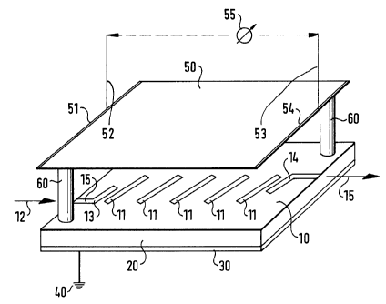
Figure 1 shows a planar band path filter on the basis of high
temperature super-conductors mounted on a dielectric substrate 20. For
better visibility, an eventually available housing is not shown. The high
temperature super-conductor layer on a lower side 30 remains unstructured
(without waveguiding structure) and operates as a ground conductor 40.
Resonators structures 11 as well as a capacitively coupled input 13 and a
capacitively coupled output 14 are formed from the high temperature super
conductor layer on the upper side by means of microstructuring methods.
A ferroelectric tuning element 50 with two electrodes 51 and 54 and
associated conductors 52 and 53 is located above a wave-guide structure
10. This ferroelectric tuning element 50 is mounted over the wave-guide
structure 10 in a corresponding distance by spacers 60 which are electrically
insulating and in some cases thermally insulating. Alternatively, the
ferroelectric tuning element 50 with its electrodes 51 and 54 and the
conductors 52 and 53 can be also mounted on the layer structure on the
housing cover or a housing side wall. The ferroelectric tuning element 50 is
provided with means for changing its temperature.
In the further text the wave-guide structure 10 identifies the unit
composed of resonator structures 11, input 13 and output 14, the filter
element identifies a unit which includes the wave-guide structure 10, a
_ 7_
CA 02206037 2001-02-07
conductor 30 and the substrate 20. The filter is a combination of the filter
element and the tuning element.
An incoming microwave signal or millimeter wave signal 12 is
reflected by the resonator structure 11. If its frequency does not coincide
with the resonance frequency of the resonance structure. Otherwise it is
transmitted, and the greater part of the wave radiation comes before the
dielectric substrate 20. Since the dielectric substrate 20 is optimized for
low
losses, which means small imaginary part of the dielectric constants as well
as good growth conditions for the superconductive layer, the damping of the
transmitted signal is very low. The filtered signal 15 is available at
capacitively coupling output 14. The resonators in this embodiment have
small difference in position and width of the own resonance. The super
position of the individual resonances provided the transmission band.
The frequency position of the individual resonances as well as
their coupling under one another are determined by the effective dielectric
function of the medium which surrounds the individual resonators. This
effective dielectric function is changed by changing the dielectric function
of
the ferroelectric element 50. For this purpose a voltage is supplied to the
ferroelectric element 50 through the conductors 52 and 53 hand the
electrodes 51 and 54. The integral influencing method shown in Figure 1
can simultaneously displace the intrisic frequency of all resonators and
-8-
CA 02206037 2001-02-07
thereby displace the transmission characteristic of the filter substantially
on
the frequency axis. Therefore, from the passive components which is a filter
element, an active component formed as an electrically tunable filter is
realized. An antiferroelectric layer can be also utilized for tuning as the
ferroelectric layer used in this embodiment.
A further preferable embodiment is shown in Figure 2. Here a
filter element is selected as a component. For better visibility, an exploded
drawing is made. Broken lines show the points which in assembled position
coincide with one another. Functionally identical components are identified
here with the same reference numerals as in Figure 1 and may not be
described in detail herein.
The filter element for this example is formed with a coplanar
technology. The superconductive layer 30 without waveguide structure
which operates as a ground conductor40 is located in the same plane as the
filter structure with its resonators 11. The functional difference from the
embodiment shown in Figure 1 is the ferroelectric or antiferroelectric tuning
unit. The ferroelectric or antiferroelectric layer is microstructured. A
ferroelectric or antiferroelectric microstructure 200 is located over each
resonator. It is available via substantially small lateral size ~ as the
associated resonator. Also, a ferroelectric or antiferroelectric structure201
is associated over each intermediate space between two resonators. Its size
_g_
CA 02206037 2001-02-07
is selected so that it overlaps insignificantly with the superconductive
resonators. All ferroelectric or antiferroelectric elements can be produced
from the same layer by microstructuring methods. However, they can also
be composed of different materials, in particular combined ferroelectric-
antiferroelectric material.
Each of these compensating elements is available through a
respective electrode pair 51 and 54, through which a voltage can be applied.
By different voltages applied at the corresponding compensating element or
by special material selection and corresponding dielectric constants because
of the same applied voltage, the effective dielectric constants can be
changed not integrally but also locally. Thereby each intrinsic frequency of
each resonator as well as each coupling between neighboring resonators
can be adjusted separately. By compressing or spreading of the intrinsic
frequency set of the resonators the filter characteristic can be adjusted to
be
a substantially small band or a substantially broad band characteristic. By
changing the coupling, the three reflectance additional maxima in a
transmission band can be reinforced or weakened.
A deviation of this embodiment is provided by the combination
of the features of both previous examples, in which a part of the re~ onators
is tuned individually while another part of the resonators is tuned
integrally.
-90-
CA 02206037 2001-02-07
A further embodiment is shown in Figure 3. Those parts of this
embodiment which are similarto the parts of the preceding embodiments are
identified with the same reference numerals and are not described in detail.
The filter element of Figure 1 in microstrip conductor structure, here
composed of only three resonators, is located in a.housing which is partially
sectioned for reasons of better understanding and has an upper wall 12 .
Massive ferroelectric or antiferroelectric bodies 100, 101, 102 are located
above the filter element 10 and mounted by screws 110, 111, 112 on the
housing cover to be adjustable as to their height. Also, the later adjustment
is also possible as selected for the ferroelectric or antiferroelectric body
103,
which is connected by a screw 113 with the side wall 130 of the filter
housing. The adjustment of the filter characteristic is performed with the
same principle as in the embodiment shown in Figure 2. However, a
contribution of the ferroelectric or antiferroelectric element to the
effective
dielectric constant because of the greater volume portion is higher, and
results in a broader adjustment region. Also, a further adjusting parameter
is available with the distance between the wave-guide and ferroelectric and
antiferroelectric element. Thereby a greater preadjustment can be
performed by placing the individual adjusting elements. The fine
compensation as well as a post guidance of the filter characteristic which is
required in the course of the drift phenomena, can be performed in electrical
:~
way through the ferroelectric or antiferroelectric elements.
_77_
CA 02206037 2001-02-07
A deviation of this embodiment resides in that the
antiferroelectric or ferroelectric interference body is mounted with piezo-
translators instead of screws. Thereby an exclusively electric adjustment of
the filter is performed.
A further deviation of this embodiment resides in that the
antiferroelectric or ferroelectric interference body is mounted rigidly on the
housing inner surface without additional mechanical position adjustment. If
the flexibility of the electrical adjustment suffices by changing the
dielectric
constant, a mechanically simple mounting is obtained.
A further deviation of the above mentioned embodiments is
based on the recognition that the dielectric constant of the ferroelectric or
the
antiferroelectric in the vicinity of the phase transition has a strong
temperature dependence. Thereby the electrical control of the effective
dielectric constant of the environment of the filter element can be realized,
also indirectly by a device for adjusting the temperature of the tuning
element.
It will be understood that each of the elements described
above, or two or more together, may also find a useful applicatio ~ in other
types of constructions differing from the types described above.
-92-
CA 02206037 2001-02-07
While the invention has been illustrated and described as
embodied in planar filter with ferroelectric andlor antiferroelectric
elements,
it is not intended to be limited to the details shown, since various
modifications and structural changes may be made without departing in any
way from the spirit of the present invention.
Without further analysis, the foregoing will so fully reveal the
gist of the present invention that others can, by applying current knowledge,
readily adapt it for various applications without omitting features that, from
the standpoint of prior art, fairly constitute essential characteristics of
the
generic or specific aspects of this invention.
What is claimed as new and desired to be protected by Letters
Patent is set forth in the appended claims.
-13-