Note: Descriptions are shown in the official language in which they were submitted.
CA 02206089 2003-10-09
APPLICATION NUMBER 2,206,089
Inventor: Manvel Zakharian
METHOD OF OBTAINING THE ADJUSTABLE CAPACITOR
BACKGROUND OF THE INVENTION
The present invention relates to the methods of obtaining the adjustable
capacitor for low-
voltage and high-voltage.
Known mechanical method of obtaining an adjustable capacitor uses the step of
changing a
distance between capacitor plates or the step of changing an active area of
capacitor plates. This
method has following shortcomings:
It is not expedient to use a mechanical method for capacitors with a big
capacity, for high-
voltage capacitors, for Vacuum Capacitors and for Gas Capacitors;
It is not possible to use a mechanical method for changing capacities of
Electrolytic
Capacitors which plates are realized as spirals;
The peak of energy density is not high.
US Patent No 3,569,795, C1.317/231 of Gikow is an example of well known
voltage variable
capacitors of alternating current in which a capacity of a capacitor is
changed as a result of the effect
of changing a dielectric constant of a ferroelectric material by direct
current control voltage. The
capacitors of this type have relatively narrow range of changing a capacity
and the used principle of
changing a capacity cannot transform other types of capacitors into variable
capacitors.
Gikow, in US Patent No 3,562,637, C1.323/74, uses direct current control
voltage, applied to
each capacitor from a plurality of capacitors (at least four capacitors), for
obtaining the adjustable
capacitor of alternating current. The control voltage creates on each of the
pairs of said capacitors,
connected together in series, voltages which have opposite directions and
counteract each other. In
this technical solution all energy of charging of said serially connected
capacitors cannot be
discharged and the energy, which cannot be discharged, is approximately
proportional to (CU~)2
where U~ is the control voltage, C is the capacitance of one of said
capacitors. The mentioned
shortcomings decrease the range of changing the capacity. Said plurality of
capacitors cannot
provide a rapid extraction of the stored energy into a load because voltages
on each of the pairs of
said capacitors have opposite directions and the electric charges on each of
the two connected
together plates of said capacitors are the same: positive or negative: For
obtaining the adjustable
capacitors according to both Gikow US Patents No 3,562,637 and No 3,569,795,
it is necessary to
use a source of control voltage of direct current with resistors and
recuperate relatively high energy
losses on said resistors.
In US Patent No 5,600,187, C1.307/157, El-Hamamsy et al. (for obtaining the
adjustable
capacitor of alternating current) use direct current bias control voltage
applied to drain and source
terminals of a MOSFET, having a body diode integral therewith, whose gate and
source terminals
are connected together, where said MOSFET is connected in series with a
capacitor C ~ and the
1
CA 02206089 2003-10-09
voltage of operating electric circuit of alternating current is applied to
said serially connected
MOSFET and capacitor. The output capacitance of said MOSFET comprises the sum
of its drain-to-
source capacitance and its drain-to-gate capacitance. According to El-Hamamsy
et al, both of these
interelectrode capacitances vary with the control voltage of direct current
applied to drain and
source terminals of said MOSFET. As the control voltage increases, the
interelectrode capacitances
decrease, thus decreasing the total capacitance between terminals. In this
Patent the capacitor C ~ is
utilized as a protective device which prevents significant power losses. For
obtaining a variable
capacitor El-Hamamsy et al. use the conception of changing drain-to-source
capacitance and drain-
to-gate capacitance of a MOSFET by said control voltage of direct current.
This conception has
following shortcomings:
- It has very narrow technical applicability and according to El-Hamamsy et
al, the technical
solutions of US Patent 5,600,187 are useful as a tuning capacitor in an
electrodeless HID lamp
ballast;
- The peak of energy density is not high;
- It can be utilized only for obtaining a variable capacitor of picofarad
values;
- It cannot be utilized for obtaining a variable Electrolytic Capacitor, etc.
Examples of switching capacitor without moving parts are described in US
Patent No
3,778,645, C1.307/318. This invention includes the steps of connecting a
tunneling capacitor in
series with in parallel connected an invariable resistor and a second
capacitor; applying a bias
potential to said tunneling capacitor. As a result of applying a bias
potential to said tunneling
capacitor, the tunneling current increases exponentially and capacitance is
changed from a first value
to a second value. A pulse direct current voltage source is utilized for
applying said bias potential.
Technical solutions of the Patent No 3,778,645 do not include a switching
device connected to said
tunneling capacitor. The equivalent circuit is presented with a switching
device SWZ (FIG.3) for
explaining creation of a tunneling current by said tunneling capacitor and by
said applied bias
potential. In the Patent No 3,778,645, one cannot find the following
information: is said tunneling
capacitor larger or smaller in comparison with said second capacitor?; is said
resistor connected in
parallel with larger or smaller of said capacitors? This method has following
shortcomings:
The pulse direct current voltage source affects the value and the form of
operating
alternating voltage, during applying the bias potential;
It cannot be utilized in an operating circuit of direct current because said
method cannot
provide a rapid extraction of all stored energy into a load;
Used principle of changing a capacity cannot smoothly change a capacitance and
cannot
transform other types of capacitors into variable capacitors;
The tunneling current increases energy losses. It is also necessary to
underline that the
technical solutions, presented in the Patent No 3,778,645, can only function
with said tunneling
capacitor whose structure is described in the claims 2, 3 and 7 of said
Patent.
A conception which permits transforming all types of invariable capacitors of
direct current
into adjustable capacitors with stepless control of capacity does not exist in
the art and an adjustable
Electrolytic Capacitor does not exist on the market.
A conception which permits obtaining voltage drop devices (for a serially
connected load)
with stepless voltage drop control, without energy losses (practically) and
which can replace variable
resistances does not exist in the art.
2
CA 02206089 2003-10-09
SUMMARY OF THE INVENTION
The present invention includes the new conception of changing the total stored
energy of at
least two capacitors or at least two groups of capacitors which are connected
in series. The
expressions from ( 1 ) to ( 10), described in the detailed description of the
invention, are the theoretical
base of said new conception. The invention permits transforming all types of
invariable capacitors of
direct current into adjustable capacitors and providing broad ranges of
changing a capacity of the
adjustable capacitor without changing their mechanical structure. The
mentioned conception is
realized by the steps of
choosing the capacity of a first capacitor or a first group of capacitors,
which has first and second
output terminals, no more than the capacity of a second capacitor or a second
group of capacitors
which has first and second output terminals;
connecting at least said first and second capacitors or said first and second
groups of capacitors in
series;
connecting capacitor plates of said first capacitor or said first and second
output terminals of said
first group of capacitors through at least one cell, which changes its
resistance or reactance, and/or
at least one switching device and/or at least one adjustable resistance device
andlor at least one
adjustable reactance device;
then converting at least one of said cells or switching devices or adjustable
resistance devices or
adjustable reactance devices into a non-conducting state or into a state with
higher impedance within
charging of said second capacitor or said second group of capacitors;
and then connecting electrically the capacitor plates of said first capacitor
or said first and second
output terminals of said first group of capacitors.
It is possible to change a capacity of the adjustable capacitors differently:
- by changing the duration of a period of time when at least one of said cells
or switching
devices or adjustable resistance devices or adjustable reactance devices is in
a non-conducting state
or in a state with higher impedance;
- by changing a value of resistance and/or reactance of supplementary
adjustable cell and/or
supplementary adjustable resistance or reactance device(s);
- by changing a value of a voltage of voltage source.
Another object of the invention is to obtain Adjustable Electrolytic
Capacitors, Vacuum
Capacitors, Gas Capacitors, Ceramic Capacitors, Mica Capacitors, etc. which
can be easily
manufactured. This third object is attained by step of
combining a capacitor plate of said first capacitor with a capacitor plate of
said second capacitor,
which have the same potential, or combining the capacitor plates of said first
group of capacitors
with the capacitor plates, which have the same potential, of said second group
of capacitors.
Another object of the invention is to obtain Vacuum and Gas adjustable
capacitors with the
higher energy density. This fourth object is attained by the by steps) of
making the area of the non-combined capacitor plate or plates of said first
capacitor or said first
group of capacitors smaller than the area of said combined capacitor plate or
said combined
capacitor plates;
and/or installing said all capacitor plates in a hermetic volume;
filling said hermetic volume by at least a gas with a higher pressure than the
atmospheric pressure or
creating a vacuum in said hermetic volume with a pressure between 10 g and 0,6
Pa.
3
CA 02206089 2003-10-09
Another object of the present invention is to obtain adjustable capacitors
which can multiply
a voltage of said voltage source. This fifth object is attained by steps of
choosing 2n (where n = 1, 2, 3, 4, ... etc) other capacitors or 2n other
groups of capacitors, each 2
of said 2n other capacitors or each 2 of said 2n other groups of capacitors
having capacities equal to
capacities of said first and second capacitors respectively or equal to
capacities of said first and
second groups of capacitors respectively,
or choosing 2n (where n = l, 2, 3, 4, ... etc) other capacitors or 2n other
groups of capacitors;
repeating on each 2 of said other capacitors or on each 2 of said other groups
of capacitors all steps
which are realized with said first and second capacitors or all steps which
are realized with said first
and second groups of capacitors;
connecting said first, second and said 2n other capacitors or said first,
second groups of capacitors
and said 2n other groups of capacitors in series during discharging of said
all capacitors.
Another object of the invention is to obtain adjustable capacitors of
alternating voltage which
can be utilized as voltage-drop devices with stepless control of voltage drop
and without energy
losses (practically). This sixth object is attained by steps of
connecting a third capacitor or a third group of capacitors, which has first
and second output
terminals, with said first capacitor or first group of capacitors or with said
second capacitor or
second group of capacitors in series;
removing charging of said third capacitor or said third group of capacitors by
a short circuit or by a
circuit with a low impedance during a period of time when the voltage
direction is positive;
removing charging of said first capacitor or said first group of capacitors by
a second short circuit or
by a circuit with a low impedance during a period of time when the voltage
direction is negative;
connecting capacitor plates of said third capacitor or said output terminals
of said third group of
capacitors through at least one additional cell, which changes its resistance
or reactance, or at least
one additional switching device or at least one additional adjustable
resistance device or at least one
additional adjustable reactance device;
then converting at least one of said additional cells or additional switching
devices or additional
adjustable resistance devices or additional adjustable reactance devices into
a non-conducting state
or into a state with higher impedance within charging of said second capacitor
or said second group
of capacitors;
and then connecting electrically the capacitor plates of said third capacitor
or said output terminals of
said third group of capacitors.
The objects, advantages and many other novel features of the present invention
are apparent
from the following detailed description when read in conjunction with the
appended claims and
attached drawings.
DESCRIPTION OF THE DRAWINGS
The invention is hereinafter described with reference to the accompanying
drawing in which:
-FIG.l and FIG.2 illustrate the step of connecting at least first 1 and second
2 capacitors or
first 1 and second 2 groups of capacitors in series;
-FIG.2, FIG.3, FIG.4, FIGS, FIG.6, FIG.7 and FIG.8 illustrate the step of
connecting
capacitor plates of said first capacitor 1 or said first group of capacitors 1
or their terminals through
at least one cell 3 (FIG. 3 and FIG.7), which changes its resistance or
reactance, and/or at least one
4
CA 02206089 2003-10-09
switching device 4 (FIG.4 and FIG.7) andlor at least one adjustable resistance
5 (FIG.S) and/or at
least one adjustable reactance 6 devices) (FIG.6a and FIG.6b).
As a cell, which changes its resistance or reactance can be used: a
photoconductive cell or cells 3a,
3b (FIG.B), a photoelectric cell 3 (FIG.7), a photorelay, a photodiode, a
material which changes its
resistance with changing in temperature, for example VOz .
As a switching device 4 can be used: an electronic switching device (for
example: a photo-thyristor
4, FIG.7), a triode, a thyratron, a gas-discharge switching device or a
mechanical switching device
when electric charge time constant of the second capacitor 2 or the second
group of capacitors 2 is
big;
-FIG.9, FIG.10 and FIG.42 explain the steps of changing a capacity of the
adjustable
capacitor by changing the duration of a period of time when at least one of
said cells or the switching
device 4 is in a non-conducting state;
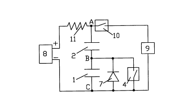
-FIG.11, FIG.12 and FIG.15 explain the steps of connecting a voltage source 8
to the
capacitor plates (which do not have the same potential) of said first 1 and
second 2 capacitors or to
output terminals (which do not have the same potential) of said first 1 and
second 2 groups of
capacitors through at least one supplementary cell (which changes its
resistance or reactance) and/or
through at least one supplementary adjustable resistance 12 or reactance 13
devices; and changing a
capacity of the adjustable capacitor by changing a value of resistance and/or
reactance of said
supplementary adjustable cell andlor said supplementary adjustable devices) 12
and 13. FIG.15
explains process of charging the second capacitor 2 or process of charging the
second group of
capacitors 2 when the resistance 12 has different values. A switching device
10 of a load 9 provides
discharge of said capacitors in demanded time;
-FIG.13 and FIG.14 explain the steps of connecting the capacitor plates (which
do not have
the same potential) of said first 1 and second 2 capacitors or said output
terminals (which do not
have the same potential) of said first 1 and second 2 groups of capacitors
through a voltage source 8;
connecting a load 9 to the capacitor plates (which do not have the same
potential) of said first 1 and
second 2 capacitors or to said output terminals (which do not have the same
potential) of said first 1
and second 2 groups of capacitors through a threshold switch 14; choosing the
maximum voltage of
the voltage source 8 more than the started voltage of the threshold switch 14;
and changing a
capacity of the adjustable capacitor by changing a value of a voltage of said
voltage source 8. As a
threshold switch 14 can be used a spark gap;
-In FIG.9, FIG.10, FIG.11 and FIG.13 said step of connecting electrically the
capacitor
plates of the first capacitor 1 or the first group of capacitors 1 (FIG.10),
is realized through at least
one diode 7 which is installed against current of charging of the first
capacitor 1 or the first group of
capacitors 1. A thyristor 4-2 (FIG.14), with control unit 15, can be used
instead of the diode 7;
-FIG.16 explains the steps of detecting the voltage of the first capacitor 1,
by a detector of
voltage 17, within its discharging; receiving signals of detecting and using
said signals ( by a control
unit 18 of an arrester 4-2) in the step of connecting electrically the
capacitor plates of the first
capacitor l;
-In FIG.17, FIG.18, FIG.19, FIG.20, FIG.21, FIG.22, FIG.23, FIG.24, FIG.25,
FIG.26 and
FIG.27 the first l and second 2 capacitors have a combined plate 20 or
combined plates 20. These
realizations include: non-combined capacitor plates 19 and 21 of the first l
and the second 2
capacitors; an insulator 22 of the first capacitor 1; an insulator 23 of the
second capacitor 2; an
insulator 24; insulators 25 and 26 of a gas or a vacuum adjustable capacitor;
a chamber 27; an
opening 28; coolers 29 and conductors 30;
-FIG.28 and FIG.29 explain the steps which multiply a voltage of the voltage
source 8 and
ensure high ranges of changing the capacity of the adjustable capacitor. These
realizations include:
CA 02206089 2003-10-09
two other capacitors 1-l and 2-2; arresters 31 and 32; at least one diode 33;
resistances R;
switching devices 4-1 and 4-3; arresters 4-2 and 4-4 and diode 7-2. As an
arrester can be used a
spark gap;
-FIG.30 and FIG.31 illustrate the step of connecting the first 1, second 2 and
a third 34
capacitors or the first 1, second 2 and third 34 groups of capacitors in
series;
-FIG.31, FIG.32, FIG.33, FIG.34 and FIG.35 illustrate the step of connecting
capacitor
plates of the third capacitor 34 or the third group of capacitors 34 or their
terminals through at least
one additional cell 3A (FIG.32), which changes its resistance or reactance,
and/or at least one
additional switching device 4A (FIG.33), and/or at least one additional
adjustable resistance SA
(FIG.34), and/or at least one additional adjustable reactance 6A (FIG.35)
device(s);
-FIG.36, FIG.37, FIG.38 and FIG.39 explain the steps which are necessary for
obtaining the
adjustable capacitor in an electric circuit of alternating voltage. These
realizations include: an
additional switching device 4A; a voltage source 35, a switching device 36 and
a rectifier 37;
-In FIG.40 the third group of capacitors 34 is connected with the second group
of capacitors
2 in series;
-In FIG.41 the third 34 and the second 2 capacitors have combined plates 21.
These
realizations include non-combined capacitor plates 38 and an insulator 39 of
the third capacitor;
-FIG.42 illustrates a second realization which ensures changing the capacity
of the adjustable
capacitor by changing the duration of a period of time when at least one cell
is in a non-conducting
state or in a state with higher impedance. This realization includes: a
transistor switch 49 with
resistances 40, 41 and 42; an adjustable resistance 43; a capacitor 44; a
photoconductive cell 45; a
threshold switch 46; triggers 47 and 50; light sources 48 and 51.
DETAILED DESCRIPTION OF THE INVENTION
The method of achieving the purpose of changing a capacity of the adjustable
capacitor, by
changing the duration of a period of time when the switching device 4 is in a
non-conducting state, is
demonstrated below for the realization shown in FIG.9.
tp (FIG.15) is a moment of switching on the voltage source 8. In the moment tp
or before the
moment tp , the step of connecting the capacitor plates of the first capacitor
1 is realized by
switching on the switching device 4. In a moment t1 (FIG.15), the step of
converting the switching
device 4 into a non-conducting state is realized by switching off the
switching device 4. The charging
of the first capacitor 1 begins at this moment t1 .
A period of time Ot, when the switching device 4 is in a non-conducting state,
within
charging of the second capacitor 2, is given by the following condition:
O <_ of <_ 52 (1)
where: RI ~ X C2 = 'C is electric charge time constant of the second capacitor
2; RI ~ is the
resistance of the resistance 11 (FIG.9); C2 is the capacity of the second
capacitor 2.
In a moment tF (tF - tp < SRI I X C2), the process of charging the capacitors
1 and 2 is finished.
At this moment tF or later in a moment t2 , the step of discharging the
adjustable capacitor is
started by switching on the switching device 10 (FIG.9). In a moment t3
(FIG.15), the process of
discharging the first capacitor 1 is finished and the step of connecting
electrically the capacitor plates
of the first capacitor 1 is realized by diode 7.
6
CA 02206089 2003-10-09
During a period of time ~t2 = tq - t3 , the step of discharging the second
capacitor 2 is realized
through the diode 7. In a moment ~ , the process of discharging the second
capacitor 2 is finished.
In this moment t~ , described above process of charging the adjustable
capacitor can be repeated by
switching offthe switching device 10.
In case of ~t = SRl1 X C2 , the capacity of the adjustable capacitor CA is
given by
following expression:
CA - ~ C 1 X C2 ~ ~ ~C 1 + C2
where Cl and C2 are the capacities of the first 1 and the second 2 capacitors.
In case of ~t = 0, the capacity of the adjustable capacitor CA is given by
CA - C2
Therefore, by changing the duration of the period of time Ot (when the
switching device 4 is in a
non-conducting state) one can change the capacity of the adjustable capacitor
CA within limits:
( C I X C2 ~ ~ ~C 1 + C2 ) ~ CA ~ C2
After finishing process of charging the adjustable capacitor, the energy of
the adjustable
capacitor WA and voltages of capacitors are given by the following
expressions:
WA - C, x U~2 ~ 2 + C2 x UZZ ~ 2 (5)
Us - Ui + UZ t6)
WA - CA X ( U~ ~ U2 ~ 2 ~ 2 (7)
U, - 1~ C, X y x dt (8)
Where: U~ and U2 are the voltages of the first 1 and the second 2 capacitors;
US is the voltage
of the voltage source 8; CA is the capacity of the adjustable capacitor; 1
instantaneous current; ~t
the duration of a period of time when the switching device 4 is in a non-
conducting state.
In case of C~ < C2 , it follows from above expressions (4), (S), (6), (7), (8)
that:
- the more C2 / C ~ the more range of changing CA ;
- in case of Ot = 5'L, CA is of the order of C ~ ;
- the more Ot the less CA ;
Consequently, in case of C2 / C ~ = 10 one can change C A approximately 11
times, in case of
C2 / C 1 = 1000 one can change CA approximately 1000 times etc.. Mentioned
results are the
same for the first 1 and the second 2 groups of capacitors connected in series
(FIG.10 and FIG.9).
Therefore, the method offered provides the revolutionary broad ranges of
changing the capacity of
the adjustable capacitor.
7
CA 02206089 2003-10-09
The method of achieving the purpose of changing a capacity of the adjustable
capacitor,
by changing a value of the supplementary adjustable resistance 12 or the
supplementary adjustable
reactance 13, is demonstrated below for the realization shown in FIG.1 l and
FIG.12.
Achieving this purpose includes the step of connecting a voltage source 8 to
the capacitor plates,
which do not have the same potential, of the first 1 and the second 2
capacitors through at least one
supplementary adjustable resistance 12 and/or at least one supplementary
adjustable reactance 13
device(s).
Curves 1, 2 and 3 (FIG.15) demonstrate the process of charging the second
capacitor 2 (FIG.11)
when the switching device 4 is in a conducting state. Dotted lines 1, 2 and 3
(FIG.15) demonstrate
the process of charging the second capacitor 2 (FIG.11) when the switching
device 4 is on all the
time when charging the second capacitor 2. The values of supplementary
adjustable resistance 12 for
curves 1, 2 and 3 are respectively equal to R 12_i , Rt2_2 arid R12-3 . Their
values are given by
conditions
R12-3 ~ Rl2-2 ~ R12-1
R12-~ = R1 t (9)
When the switching device 4 is in a conducting state the process of charging
the second capacitor 2
is given by following expression
U - U X ( 1 _ e-t/R,zXc2) (l0)
where Rt2 is the resistance of the resistance 12 (FIG.11 ).
U2-t ~ U2-2 ~d U2-3 (FIG.15) are the voltages of the second capacitor 2 when
Rt2 is respectively
equal t0 Rt2_1 , R12-2 ~d Rt2-3 .
It follows from above expressions (5), (6), (7), (10) that:
- the more Rt2 the less the voltage U2 (FIG.15) in the same moment of the
process of
charging C2 ;
- the more Rt2 the less CA , when the step of converting the switching device
4 into a
non-conducting state is realized after the same time delay ~tl , for example:
~t~ = t~ - tp (FIG.15).
Consequently, one can change the capacity of the adjustable capacitor Cp by
changing the value of
the supplementary adjustable resistance 12. In case of changing the capacity
of the adjustable
capacitor by changing a value of the supplementary adjustable reactance 13
(FIG.12) there is not
energy loss.
The method of achieving the purpose of changing a capacity of the adjustable
capacitor,
by changing the value of a voltage of the voltage source 8 is demonstrated
below for the realization
shown in FIG.13 and FIG.14. Achieving of purpose includes the steps of
connecting the capacitor plates of the first 1 and the second 2 capacitors
through the voltage source
8;
connecting a load 9 to the capacitor plates of the first 1 and the second 2
capacitors through a
threshold switch 14;
choosing the maximum voltage of the voltage source 8 more than the started
voltage of the threshold
switch 14.
8
CA 02206089 2003-10-09
The values of voltages are given by following conditions:
Us ' Ua ( 11 )
Us - Ut + U2 ( 12)
where UB is the started voltage of the threshold switch 14 which for this
realization equal to the
breakdown voltage of the arrester 14.
It follows from above expressions (5), (7), ( 10), ( 11 ), ( 12) that:
- the more US the more U2 in a moment t1 when the step of converting the
switching
device 4 into a non-conducting state is realized by switching off the
switching device 4;
- the more US the less U1 in a moment of breakdown of the arrester 14;
- the more US the more CA when the step of converting the switching device 4
into a non-
conducting state is realized in the same moment, for example in a moment t1
(FIG.15).
Consequently, one can change the capacity of the adjustable capacitor CA by
changing the
value of a voltage of the voltage source 8.
In case of a big discharging current, the step of connecting electrically the
capacitor plates of
the first capacitor 1 can be realized by the thyristor 4-2 (FIG.14) or the
arrester 4-2 (FIG.16).
When the adjustable capacitor must be discharged during a period of time,
which is of the order of
microseconds and less, the step of connecting electrically the capacitor
plates of the first capacitor 1
is realized by the arrester 4-2 (FIG.16), with a starting electrode 16, or can
be realized by a triode or
a thyratron. The control unit 18 of the arrester 4-2 forms trigger pulses for
the starting electrode 16.
The control unit 18 can have 4 or 5 terminals (fifth terminal is showed as a
dotted line). The step of
detecting the voltage of the first capacitor 1 (FIG.16) within it discharging
is realized by the detector
of voltage 17. The control unit 18 of the arrester 4-2 uses the signals of
detecting in the step of
connecting electrically the capacitor plates of the first capacitor 1. In a
moment t3 (FIG.15), the
arrester 4-2 is in a conducting state.
The step of combining a capacitor plate of the first capacitor 1 with a
capacitor plate of the
second capacitor 2, which have the same potential, is demonstrated below for
the different
realizations:
1. The area of the combined capacitor plate 20 is equal to the area of each of
the non-
combined capacitor plates 21 and 22 (FIG.17);
2. The area, of the non-combined capacitor plate 19 (FIG.18, FIG.20, FIG.21,
FIG.22) or
plates 19 (FIG.19, FIG.26, FIG.27) of the first capacitor or the first group
of capacitors, is realized
smaller than the area of the combined capacitor plate 20 or the combined
capacitor plates 20. This
step, in case of using the same insulators 22 and 23 (examples: Oil
Capacitors, Gas Capacitors,
Vacuum Capacitors ), ensures minimal dimensions;
3. The area of the combined capacitor plates 20 is realized bigger than the
area of each of the
non-combined capacitor plates 19 and 21 (FIG.19, FIG.20, FIG.21, FIG.22,
FIG.26, FIG.27). This
step ensures a high peak of energy density of the adjustable capacitor;
4. All capacitor plates are realized as spirals (FIG.20, FIG.21, FIG.22). This
step ensures a
high peak of energy density of the adjustable capacitor, for example a high
peak of energy density of
Electrolytic adjustable capacitor (in this time an Electrolytic adjustable
capacitor does not exist);
5. The area of the combined capacitor plate 20 is realized smaller than the
area of each of the
non-combined capacitor plates 19 and 21 (FIG.23, FIG.24, FIG.25). This step
permits to change the
9
CA 02206089 2003-10-09
capacity of the adjustable capacitor CA smoothly within a range which is of
the order of C2 .
Constructions of the first and second capacitors can have two or more combined
plates (FIG.25) and
two or more dii~erent ranges of changing CA ;
6. The realizations shown in FIG.17, FIG.18, FIG.23, FIG.24 and FIG.25 include
the step of
isolating the capacitor plates 19 and 20 of the first capacitor by at least
one insulator 22 which has
lesser permittivity than the permittivity of the insulator 23 (FIG.17) of the
capacitor plates of the
second capacitor or insulators 23 and 24 (FIG.23). As insulators 23 and/or 24
can be used
BaSn03 , BaZr03 , CaTi03 , etc. which have big permittivity. The step of
isolating the capacitor
plates 19 and 20 of the first capacitor by insulator 22, which has lesser
permittivity than the
permittivity of the insulator 23 (FIG.17) and/or insulator 24, ensures the
lowest cost price and broad
ranges of the capacity of the adjustable capacitor CA ;
7. The steps of installing said all capacitor plates in a hermetic volume,
filling said hermetic
volume by at least a gas with a higher pressure than the atmospheric pressure
or creating a vacuum
in said hermetic volume with a pressure between 10 g and 0,6 Pa, ensure a high
peak of energy
density of Gas and Vacuum Capacitors because:
- between the vacuum pressure about 0,6 Pa and the atmospheric pressure, the
electric
strength of vacuum is less than 30 kV/cm;
- the electric strength of the air, in case of normal atmospheric pressure, is
about 30 kV/cm;
- the more pressure of the air the more the electric strength of the air. For
example, the
electric strength of the air is about 380 kVlcm, in case of the pressure of
the air about 15
atmosphere;
- the less a vacuum pressure (less than 0,6 Pa) the more the electric strength
of a vacuum.
For example, the electric strength of the vacuum, with the pressure about
0,001 Pa, is about 200
kVlcm.
The step of creating a vacuum with a low pressure ensures a high peak of
energy density of the
adjustable capacitor. It is possible to create a vacuum with a pressure about
10 g Pa.
The opening 28 (FIG.26, FIG.27) is closed after creating a vacuum inside of
the chamber 27 or the
opening 28 is closed after filling the chamber 27 by at least a gas (for
example: by the gas H2 ) with
a higher pressure than the atmospheric pressure.
8. The step of cooling the capacitor plates by a cooling system or coolers 29
(FIG.27),
installed outside of the hermetic volume, increases allowable frequency of
charging and discharging
the adjustable capacitor. Said coolers are connected to capacitor plates 19,
20 and 21 by thick
conductors 30 (FIG.27), which have a high thermal conductivity (for example
Cu). For vacuum
capacitors, this step of cooling is more necessary. One can use a coolant for
cooling the capacitor
plates 19, 20 and 21. In this case, the plates 19, 20 and 21 can have hermetic
passages for the
coolant (inside themselves).
It follows from the above constructions that the step of combining a capacitor
plate of the
first capacitor with a capacitor plate of the second capacitor or combining
the capacitor plates of the
first group of capacitors with the capacitor plates of the second group of
capacitors ensures the
lowest cost price of manufacturing the first 1 and the second 2 capacitors.
The steps of choosing at least two other capacitors 1-1 and 2-2 (the
capacities of said other
capacitors 1-l and 2-2 can be equal to the capacities of said first 1 and
second 2 capacitors
respectively), connecting said other capacitors 1-1 and 2-2 in series (FIG.28
and FIG.29), repeating
on the capacitors 1-1 and 2-2 all steps which are realized with the first l
and the second 2 capacitors,
CA 02206089 2003-10-09
connecting the first 1, the second 2 and other capacitors 1-1, 2-2 in series
during discharging of said
all capacitors l, 2, 1-1 and 2-2 ensure;
obtaining a voltage UL on a load 9 about two times more than a voltage US of a
voltage source 8
with the revolutionary broad ranges of changing a capacity of the adjustable
capacitor CA .
UL ~ 2US ( 13 )
When the number of other capacitors is equal to 2n (where n = 2, 3, 4, 5 ...,
etc.
U~~US x ( 1 +n) {14)
The step of connecting the first 1, the second 2 and the other capacitors 1-1,
2-2 in series and
the step of discharging all capacitors 1, 2, 1-1 and 2-2 are realized by
switching on the arrester 31
because:
2US > Ug_32 (15)
where U B_32 is the breakdown voltage of the arrester 32.
The step of repeating on the capacitors 1-1 and 2-2 all steps which are
realized with the first
1 and the second 2 capacitors is realized by the switching device 4-3 and the
diode 7-2 (FIG.28) or
by the switching device 4-3 and the arrester 4-4 (FIG.29). The realization in
FIG.29 ensures equal
conditions of charging the first 1, the second 2 capacitors and the other 1-1,
2-2 capacitors.
Therefore, the step of repeating, on the capacitors 1-1 and 2-2 all steps
which are realized with the
first 1 and the second 2 capacitors, can be realized in the same time with the
steps on the first l and
the second 2 capacitors. The diode 33 ( FIG.29) protects the voltage source 8
during discharging of
all said capacitors.
Ug_33 > 2US ( 16)
where Ug_33 1S the breakdown voltage of the diode 33.
Known Marx Generators cannot change the capacity of capacitors. Consequently,
the
described above steps ensure transformation of all types of Marx Generators
into new Generators
with the revolutionary broad ranges of changing capacities of Generators.
The method of obtaining the adjustable capacitor for alternating voltage, in
which said steps
of charging and discharging said capacitors or said groups of capacitors are
realized through at least
one load, is demonstrated in FIG.36.
The method of obtaining the adjustable capacitor for alternating voltage, in
which said steps
of charging and discharging said capacitors or said groups of capacitors are
realized through at least
one load and rectifier, is demonstrated in FIG.39.
FIG.38a demonstrates an alternating voltage of the voltage source 35. Curve 1
(FIG.38b)
demonstrates charge variation Q of the second capacitor 2. Dotted line 2
demonstrates charge
variation Q of the second capacitor 2 when the switching device 4 and 4A are
on all the time when
charging the second capacitor.
The method of obtaining the adjustable capacitor for alternating voltage is
demonstrated
below.
The third capacitor 34 is connected in series with the first capacitor 1
(FIG.36, FIG.39). In a
moment tp (FIG.38a), the step of connecting the capacitor plates of the third
capacitor 34 by a first
short circuit, during a period of time when the voltage direction is positive,
is realized by switching
on the additional switching device 4A. In this moment tp , the step of
connecting the capacitor plates
of the first capacitor 1 is realized by switching on the switching device 4.
tp is a moment of
switching on the voltage source 35. The charging of the second capacitor 2
begins at this moment tp
11
CA 02206089 2003-10-09
(FIG.38b). In a moment t1 (FIG.38a), the step of converting the switching
device 4 into a non-
conducting state is realized by switching off the switching device 4. The
charging of the first
capacitor 1 begins at this moment ti . In a moment t2 , the process of
charging the capacitors l and
2 is finished and the process of discharging the capacitors 1 and 2 is
started. In a moment t3
(FIG.38b), the process of discharging the first capacitor 1 is finished and
the step of connecting
electrically the capacitor plates of the first capacitor 1 is realized by the
diode 7. During a period of
time ~t2 = tq - t3 , the step of discharging the second capacitor 2 is
realized through the diode 7.
In a moment tq , the process of discharging the second capacitor 2 is
finished. In this moment to ,
the step of connecting the capacitor plates of the first capacitor 1 by a
second short circuit during a
period of time when the voltage direction is negative is realized by switching
on the switching device
4. The charging of the second capacitor 2 begins at this moment t4 (FIG.38b).
During a period of
time ~t3 = tg - t4 , the step of connecting the capacitor plates of the third
capacitor 34 through
the additional switching device 4A is realized because the additional
switching device 4A is in
switching on state. In a moment 1~ (FIG.38b), the step of converting the
additional switching device
4A into a non-conducting state is realized by switching off the additional
switching device 4A. The
charging of the third capacitor 34 begins at this moment tg . In a moment t6 ,
the process of
charging the capacitors 2 and 34 is finished and the process of discharging
the capacitors 2 and 34 is
started. In a moment t~ (FIG.38b), the process of discharging the third
capacitor 34 is finished and
the step of connecting electrically the capacitor plates of the third
capacitor 34 is realized by the
additional diode 7A. During a period of time ~1~ = tg - t~ , the step of
discharging the second
capacitor 2 is realized through the additional diode 7A. In a moment tg , the
process of discharging
the second capacitor 2 is finished. At this moment tg , the step of connecting
the capacitor plates of
the third capacitor 34 by a first short circuit during the period of time when
the voltage direction is
positive is repeated.
Described realizations shown in FIG.36 and FIG.39 can be used for controlling
the maacimum
voltage of charging the adjustable capacitor UA . One can change UA by
changing the duration of a
period of time ti - tp and 1~ - 1~ when (FIG.38a) capacitor plates of the
second capacitor 2 are
connected by a third short circuit (the switching device 36 is on during a
period of time ti - tp and
tg r tq and the switching device 36 is off during a period of time t4 - t1 and
tg - tg . Therefore,
these realizations can be used for controlling the maximum voltage of the load
L and for changing
motor speed. In case of three phases, the realization shown in FIG.36 can be
repeated for each
phase. The branch with the first 1, second 2 and third 34 capacitors can be
connected in parallel with
voltage source 35 (FIG 37) and the load L.
The step of combining the capacitor plates of said third group of capacitors
with the
capacitor plates, which have the same potential, of said second group of
capacitors is demonstrated
in FIG.41. It is obvious that the steps illustrated in FIG.17, FIG.18, FIG.19,
FIG.20, FIG.21,
FIG.22, FIG.23, FIG.24, FIG.25, FIG.26 and FIG.27 can be repeated on the
combined 21 and non-
combined 38 capacitor plates of the third capacitor 34 (FIG.41). These steps
ensure the lowest cost
price ofmanufacturing the first 1, second 2 and third 34 capacitors.
12
CA 02206089 2003-10-09
The realization, shown in FIG.42, uses as a cell a photoconductive cell 3.
During a period of
time Otl = t1 - tp (FIG.15), the capacitor plates of the first capacitor 1 are
connected through the
photoconductive cell 3 because the light source 48, which is optically
connected with the
photoconductive cell 3, is on. In a moment t1 , U44 = U th-46 ~ where U44 is a
voltage of the
capacitor 44, U th-46 iS the threshold voltage of the threshold switch 46.
At this moment t1 , the trigger 47 breaks electric current of the light source
48. In a moment
tF (tF - tp < SR11 x CZ ), the process of charging the capacitors 1 and 2 is
finished. During a
period of time tF - t1 , the photoconductive cell 3 is in a state with higher
impedance. During a
period of time tF - tp , the photoconductive cell 45 is in a state with higher
impedance because the
light source 51, which is optically connected with the photoconductive cell
45, is off. In a moment tq
(FIG.15), the transistor switch 49 breaks electric current of the resistance
42 and electric current of
the light source 51 is on by the trigger 50. The photoconductive cell 45 is in
a state with low
impedance and the capacitor 44 is discharged. Therefore, the light source 48
is on. One can change
the duration of a period of time ~t = tF - t1 , when the photoconductive cell
3 is in a state with a
higher impedance, by changing the value of the resistance 43.
13