Note: Descriptions are shown in the official language in which they were submitted.
CA 02206276 1997-0~-27
"DISCHARGE LAM~ LIGHTING DEVICE"
BACKGROUND OF THE INVENTION
This invention relates to a discharge lamp
lighting device and, more particularly, to a device for
lighting such HID lamps as high pressure sodium lamp,
metal halide lamp, high pressure mercury lamp and so on
with a square wave AC power.
DESCRIPTION OF RELATED ART
For the lighting devices of the HID lamps,
ballasts of copper type and iron type have been the main
current but, in recent years, they are being replaced by
an electronic ballast employing many electronic parts for
the purpose of minimizing the weight and dimensions and
rendering to be highly functional. Such electronic
ballast shall be briefly described in the followings.
In the electronic ballast of the kind referred
to, a DC power source circuit section including a
rectifying circuit is connected to an AC power source, an
inverter circuit part for regulating and controlling a
supplied power to the lamp is connected to output end of
the DC power source circuit section, and the lamp is
connected to an output end of the inverter circuit
section.
In the electronic ballast, more concretely, the
DC power source circuit section comprises a rectifying
circuit and a capacitor, and functions to rectify and
smooth an AC voltage of AC power source into a DC voltage,
while the inverter circuit part is constituted by a
CA 02206276 1997-0~-27
voltage dropping chopper circuit, polarity inverting
circuit, igniter circuit and control circuit. The voltage
dropping chopper circuit comprises a switching element,
diode, inductor and capacitor, which are arranged for
generating at the capacitor a voltage dropped from an
input voltage with ON/OFF operation at a high frequency of
the switching element. In this case, the switching
element turned ON causes a source current to flow from the
DC power source circuit section through the switching
element and inductor to the capacitor, and the switching
element turned OFF causes a current of accumulated energy
in the inductor to flow through the capacitor and diode.
The polarity inverting circuit comprises switching
elements forming a full-bridge circuit, in which the
respective switching elements are supplying through the
control circuit to the lamp a square wave voltage of a
lower frequency in non-load state than that in lighting
state. The igniter circuit is formed by a pulse
transformer, capacitor, such switching element as a sidac
or the like voltage response element, and resistor. The
operation of this igniter circuit is briefly described
with reference to FIG. 32. In this case, the capacitor is
gradually charged by a square wave voltage produced at the
polarity inverting circuit, with a time constant
determined by the resistor and capacitor. As the voltage
of the capacitor reaches a breakover voltage of the
switching element, the switching element is turned ON, to
have an accumulated charge in the capacitor discharged
CA 02206276 1997-0~-27
through the capacitor, switching element and a primary
winding of the pulse transformer, upon which a pulse
voltage generated at the primary winding of the pulse
transformer is boosted, and a high pulse voltage (of
several kV) is generated at a secondary winding of the
pulse transformer and is superposed on a lamp voltage.
With this high pulse voltage, the lamp is made to start
its discharge and shifts to a lighting state.
The control circuit is to detect the lamp
voltage (which may be a lamp current or lamp power) to
control the ON/OFF operation of the switching elements in
response to the detected value and to regulate the power
supplied to the lamp. When this ON/OFF operation of the
switching elements is considered, the power control is
carried out normally in response to the lamp voltage (lamp
current or lamp power) in the lamp lighting state, as has
been referred to, whereas in the non-load state a constant
power control preliminarily set is performed. Now,
provided that a switching element is controlled under the
pulse width modulation (PWM) control at a constant
frequency, for example, an ON width of this switching
element (ON duty: the rate of ON period in 1 cycle of
switching) is as shown in FIG. 33 and is controlled with a
constant ON width Tl in the non-load state but, when the
lamp is lighted, the control is made with an ON width
according to the state of the lamp. Here, the ON width is
made substantially constant at a portion adjacent to a
rated lamp voltage, since the lamp power is attempted to
CA 02206276 1997-0~-27
be kept substantially constant with respect to any
fluctuation in the lamp voltage. Whether or not the state
is of non-load is discriminated by means of the lamp
voltage or the like, upon which a threshold level is set
at a higher level than the lamp voltage at the time of
normal lighting, so that the lamp voltage in a
relationship of Vla~Vl is discriminated to be of the
non-load state and the ON width is set to be constant at
Tl.
The circuit arrangement of the kind referred to
has been also disclosed in U.S. Patent No. 4,734,624.
In such well-known discharge lamp lighting
device as has been referred to, a detection of the
lighting state immediately after the lamp starting should
result in that the frequency of the square wave at a low
frequency becomes to be abruptly high (from several ten Hz
to several hundred Hz) and the ON width of the switching
element becomes also abruptly small (Tl~T0), so that there
has been a problem that, in a state where the discharging
immediately after the starting is unstable, the discharge
can hardly be maintained, the lighting is not shiftable in
smooth manner to a constant lighting, and the starting
characteristic is deteriorated.
In order to eliminate such problem, there has
been suggested in Japanese Patent Laid-Open Publication
No. 63-150895 a device in which the operation of polarity
inverting circuit immediately after the detection of the
starting of lamp discharge is sufficiently prolonged over
CA 02206276 1997-0~-27
a constant cycle in the constant lighting state(see FIG.
34). With this device, however, a pair of switching
elements on one side of the polarity inverting circuit
have to be kept in ON state for a certain fixed period, a
special control means is required to be added for this
purpose, and the control circuit has to be complicated
enough to be another problem.
Further, an improvement in the lamp starting
characteristic has been suggested in U.S. Patent No.
4,614,898, in which a high frequency power is applied to
the lamp immediately after the starting of discharge and
the power is changed to be of a low frequency after the
lighting is made stable, but the same trouble as in the
above publication arises in rendering the control circuit
to be complicated in order to produce the high frequency
power immediately after the starting of discharge. As
further measures for improving the startability of the
lamp, it has been also known to increase the energy of the
high pulse voltage (its peak value, width, pulse number
and so on), but this causes the igniter circuit to be
enlarged in dimensions and costs and cannot be the optimum
measures. Further, as measures for improving the starting
characteristic by increasing a forced current to the lamp
immediately after the start of discharge, it is possible
(a) to increase secondary voltage in non-load state, (b)
to increase the capacity of capacitor parallel to the
lamp, (c) to increase secondary short-circuit-current, and
so on. In these respects, however, (a) requires high
CA 02206276 1997-0~-27
withstand voltage parts in the inverter circuit so as to
render the circuit enlarged in the dimensions and costs
and cannot be the optimum measure; (b) renders the
capacitor to be larger in size and also a steep current
flowing immediately after the start of discharge to be
larger, so as to similarly enlarge the dimensions and
costs of the inverter circuit, and cannot be the optimum
measure; and (c) less requires any parts to be enlarged
but involves a problem that a large current has to be made
to flow to the lamp always in starting process immediately
after the start of discharge, so as to shorten the life of
the lamp.
SUMMARY OF THE INVENTION
The object of the present invention is to
provide a discharge lamp lighting device capable of
eliminating the foregoing problems and improving the
starting characteristic without causing constituent
control circuit to be complicated but with inherent life
of the lamp maintained.
In order to realize the above object, the
discharge lamp lighting device according to the present
invention which comprises an inverter circuit section
supplying a square wave AC power from a ~C power source
circuit section to a discharge lamp, and a high voltage
pulse generating means for applying a high voltage pulse
to the discharge lamp upon starting so as to have the lamp
started thereby, the discharge lamp being lighted with a
square wave AC power of a square wave frequency lower in
CA 02206276 1997-0~-27
non-load state than that in lighting state, is
characterized in that the square wave frequency is
controlled to remain at the frequency in the non-load
state for a fixed period immediately after detection of
the start of discharge of the lamp.
Other objects and advantages of the present
invention shall become clear as the description of the
invention advances with reference to preferred embodiments
of the invention shown in accompanying drawings.
BRIEF DESCRIPTION OF THE DRAWINGS
FIGURE 1 is a circuit diagram showing main
constituents of the discharge lamp lighting device in an
embodiment according to the present invention;
FIG. lA is a concrete circuit diagram employed
in the discharge lamp lighting device of FIG. l;
FIG. lB is an operational waveform diagram of
the circuit in FIG. lA;
FIG. 2 is an operational waveform diagram
immediately after the start in the embodiment of FIG. l;
FIG. 3 is a circuit diagram showing the main
constituents of the device in another embodiment according
to the present invention;
FIG. 4 is an operational waveform diagram
immediately after the start in the embodiment of FIG. 3;
2 5 FIG. 5 is a circuit diagram showing the main
constituents of the device in another embodiment according
to the present invention;
FIG. 6 is an operational waveform diagram
CA 02206276 1997-0~-27
immediately after the start in the embodiment of FIG. 5;
FIG. 7 is a circuit diagram showing the whole
arrangement of the device in another embodiment according
to the present invention;
FIG. 8 is an operational waveform diagram of the
embodiment in FIG. 7;
FIG. 9 is a circuit diagram showing the whole
arrangement of the device in another embodiment according
to the present invention;
FIG. 10 is an operational waveform diagram of
the embodiment in FIG. 9;
FIG. 11 is a circuit diagram of a source power
input section in a practical product of the discharge lamp
lighting device embodying the present invention;
FIG. 12 is a circuit diagram of a power-factor
improving section in a practical product of the discharge
lamp lighting device embodying the present invention;
FIG. 13 is a circuit diagram of a lighting
circuit section in a practical product of the discharge
lamp lighting device embodying the present invention;
FIG. 14 is a circuit diagram showing a main
circuit arrangement of the device in another embodiment of
the present invention;
FIG. 15 is a circuit diagram showing a control
circuit in the device of the embodiment shown in FIG. 14;
FIG. 16 is a waveform diagram showing the
operation of a zero current detecting cir-cuit in the
embodiment of FIG. 14;
CA 02206276 1997-0~-27
FIG. 17 is an explanatory diagram showing
circuitry characteristics of the device in another
embodiment of the present invention;
- FIG. 18 is a circuit diagram showing an
arrangement of an OFF time supervising circuit in the
embodiment of FIG. 14 of the present invention;
FIG. 19 shows waveform diagrams for explaining
the operation of the OFF time supervising circuit in FIG.
18 of the present invention;
FIG. 20 is an explanatory view showing the
relationship between a threshold value voltage and a
discharge lamp voltage in the embodiment of FIG. 14;
FIG. 21 is a circuit diagram showing the device
in another embodiment of the present invention;
FIG. 22 is a circuit diagram of a control
circuit in the embodiment of FIG. 21;
FIG. 23 is an explanatory view for control
characteristics of ON width in the embodiment of FIG. 21;
FIG. 24 is an explanatory view for the operation
of an inverting circuit in the embodiment of FIG. 21;
FIG. 25 is a circuit diagram showing another
embodiment of the present invention;
FIG. 26 is a circuit diagram of a control
circuit in the embodiment of FIG. 25;
FIG. 27 is a circuit diagram of a control
circuit in another embodiment of the present invention;
FIG. 28 is an explanatory view-for circuit
characteristics in an event when the OFF time supervising
- 10 -
CA 02206276 1997-0~-27
circuit is not operated in the device of the present
invention;
FIG. 29 is a circuit diagram of a source power
input section in a practical product of the discharge lamp
lighting device embodying the present invention;
FIG. 30 is a circuit diagram of a power-factor
improving section in the discharge lamp lighting device
embodying the present invention;
FIG. 31 is a circuit diagram of a lighting
circuit section in a practical product of the discharge
lamp lighting device embodying the present. invention;
FIG. 32 is an operational waveform diagram of a
known igniter circuit;
FIG. 33 is an explanatory view for an ON width
control in a known control circuit; and
FIG. 34 is an explanatory view for an operation
of a known polarity inverting circuit.
While the present invention shall now be
described with reference to the respective embodiments
shown in the drawings, it should be appreciated that the
intention is not to limit the present invention only to
these embodiments shown but rather to include all
alterations, modifications and equivalent arrangements
possible within the scope of appended claims.
DETAILED DESCRIPTION OF THE PREFERRED EMBODIMENTS
EMBODIMENT 1:
In FIG. 1, there is shown an arrangement of main
constituents of the discharge lamp lighting device in a
CA 02206276 1997-0~-27
first embodiment of the present invention, in which such
main circuit as shown in FIG. lA is employable. In the
instant embodiment, the device is so arranged that, even
when the start of discharge in a discharge lamp 4 is
detected by a lighting discrimination circuit 6, its
output of a detection signal is delayed for about several
seconds by means of a delay circuit 7, and a frequency of
a square wave AC power to the discharge lamp is maintained
at a frequency of the power in non-load state for several
seconds immediately after the lamp lighting. The instant
embodiment shall be further described in detail.
In FIG. 1, part of a control circuit 5 (a
control part of a polarity inverting circuit section), in
which the lighting discrimination circuit 6 compares a
lamp voltage Vla with a lighting discrimination voltage Vl
preliminarily set so that a signal of "Low" level will be
output when Vla~Vl (non-load state) and a signal of "High"
level will be output when Vla<Vl (lighting state). These
signals are provided to the delay circuit 7 so that, when
the "Low" level signal from the lighting discrimination
circuit 6 is changed to the "High" level signal, the
"High" level signal will be output as delayed by about
several seconds. Oscillators 8 and 9 oscillate to provide
signals respectively of a square wave frequency in
non-load state (several ten Hz) and of a square wave
frequency in lighting state (several hundred Hz). A
frequency change-over switch 10 connects the delay circuit
7, in response to the output signals of the circuit 7, to
CA 02206276 1997-0~-27
the oscillator 8 when the signal is of the "Low" level
(non-load state) and to the oscillator 9 when the signal
is of the "High" level (lighting state). A low frequency
driving circuit 11 subjects the signals from the
oscillators 8 and 9 to a frequency division, to produce
signals for such ON/OFF operation as shown in FIG. lB of
respective switching elements Ql-Q4 included in a polarity
inverting circuit section 21. With such circuit
arrangement as in the above, it is enabled to prevent the
discharge lamp from flickering out and to improve the
starting characteristic by means of the square wave
frequency maintained at several ten Hz in the non-load
state for several seconds immediately after the starting
of lighting in which the discharge is still unstable. In
FIG. 2, there is shown the development in waveform of the
lamp voltage Vla immediately after the start of lighting
in the present embodiment.
EMBODIMENT 2:
FIG. 3 shows a main part arrangement in a second
embodiment of the discharge lamp lighting device. The
arrangement of FIG. lA is also employable as the main
circuit of this device. In the present instance, the
polarity inversion is not performed in the non-load state
and a DC power is supplied to the discharge lamp 4. In
this case, the present embodiment is so arranged that,
even upon detection of the start of discharging in the
lamp by the lighting discrimination cireuit 6, the
detection signal can be delayed by the delay circuit 7 for
CA 02206276 1997-0~-27
about several seconds, and the DC power supplied in the
non-load state is maintained during several seconds
immediately after the lamp lighting. The present
embodiment shall be further detailed in the followings.
In FIG. 3, part of the control circuit 5
(control part of the polarity inverting circuit section)
is shown, in which a DC output section 12 is provided
instead of the low frequency oscillator 8, and other
respects of the arrangement are the same as those in the
embodiment of FIG. 1. With this circuit arrangement, the
power applied to the discharge lamp is maintained to be
the DC power in the non-load state, so that the lamp is
prevented from extinguishing and the starting
characteristic of the lamp can be improved. In FIG. 4,
the process of the lamp voltage waveform immediately after
the start of lighting in the present embodiment is shown.
EMBODIMENT 3:
FIG. 5 shows the main part arrangement of a
third embodiment is shown. As the main circuit of this
discharge lamp lighting device, the arrangement of FIG. lA
is employable. In the present embodiment, the detection
signal of the lighting discrimination circuit 6 as to the
start of discharge is delayed by the delay circuit 7 for
about several seconds, so that ON width of a switching
element Q5 will be maintained as unchanged from that in
the non-load state for several seconds immediately after
the lamp lighting. The present embodiment shall be
further detailed in the followings.
CA 02206276 1997-0~-27
FIG. 5 shows part of the control circuit 5
(control part of a high frequency switching element Q5 in
a voltage-dropping chopper circuit section 20 of FIG. lA).
ON width setting circuits 13 and 14 are to provide
respectively a constant ON width signal in the non-load
state and a variable ON width signal responsive to the
lamp voltage upon the lighting of lamp. An ON width
change-over switch 15 is provided, in accordance with the
output signals from the delay circuit 7, to connect the
circuit 7 to the constant ON width setting circuit 13 upon
receiving the "Low" level signal or to the variable ON
width setting circuit 14 upon receipt of the "High" level
signal. A high frequency driving circuit 16 receives the
signals from the ON wldth setting circuits 13 and 14, and
produces ON/OFF signals in accordance with the state of
the lamp through an incorporated PWM controller of
oscillation signals of several ten kHz. With the above
circuit, the ON width of the switching element Q5 is
maintained to be as wide as that in the non-load state for
several seconds immediately after the start of lighting in
which the discharge state is unstable, so that the
discharge lamp can be prevented from extinguishing and can
be improved in the starting characteristic. In FIG. 6,
there is shown the process of switching state of the
switching element Q5 immediately after the start of
lighting in the present embodiment, in which Tl denotes
the ON width in the non-load state and T0 denotes an ON
width corresponding to the lamp voltage immediately after
CA 02206276 1997-0~-27
the lighting.
While in the above the PWM controller of the
fixed frequency has been referred to as an example of
means for controlling the switching element Q5, this may
be a circuit for controlling the frequency with the fixed
ON width, and it should be also optimum, for example, to
maintain the frequency in the non-load state as it is for
the period of several seconds right after the lighting so
long as the frequency in the non-load state is higher than
that immediately after the lighting.
EMBODIMENT 4:
FIG. 7 shows an arrangement in a fourth
embodiment, in which, referring in conjunction with FIG.
lA, voltage dropping chopper circuit section 20 and
polarity inverting circuit section 21 are constituted by a
single full-bridge circuit 23, and FIG. 8 shows ON/OFF
operation of the switching elements Ql-Q4 in the circuit
23 and a lamp current waveform. In the followings, this
circuit shall be detailed. A pair of the switching
elements Ql and Q4 and another pair of the switching
elements Q2 and Q3 repeat -a high frequency switching as
shown in FIG. 8. That is, the switching elements Ql to Q4
as well as Q5 in FIG. lA are used to realize both of the
polarity inverting operation and the voltage dropping
chopper operation. Further, in the cycle in which the
switching elements Ql and Q4 are performing the high
frequency switching, an energy of an ind-uctor Ll is
subjected to a feedback through diodes D2 and D3 to the
- 16 -
CA 02206276 1997-0~-27
power source in the OFF state but, in another cycle in
which the switching elements Q2 and Q3 are making the high
frequency switching, the energy feedback of the inductor
Ll occurs through diodes Dl and D4 in the OFF state. That
is, these diodes Dl to D4 are performing the function of a
diode D5 in FIG. lA.
With the above operation, the same square wave
AC current as in Embodiment 1 can be obtained, and the
same control as in Embodiment 1 can be made possible.
Further, when such element incorporating the diode as FET
is employed instead of the switching elements Ql to Q4,
the function of the diodes Dl to D4 may be performed by
such elements, so that the number of the switching
elements and diodes employed can be reduced to four, in
contrast to six in the case of Embodiment 1, and the use
of FET or the like will be advantageous in the cost
reduction and dimensional minimization.
EMBODIMENT 5:
FIG. 9 shows a fifth embodiment, in which the
function of the voltage dropping chopper circuit section
20 and polarity inverting circuit section 21 in Embodiment
1 is realized by a half bridge circuit 24, and FIG. 10
shows ON/OFF operativn of the switching elements Ql and Q2
and a lamp current waveform. This circuit shall be
detailed in the followings. The switching elements Ql and
Q2 repeat such high frequency switching as shown in FIG.
10, that is, the switching elements Ql-Q4 and Q5 are used
for both purposes. Further, in the cycle in which the
CA 02206276 1997-0~-27
switching element Q1 performs the high frequency
switching, the energy in the inductor Ll is fed back
through the diode D2 to a capacitor C4 in the OFF state,
and, in the cycle in which the switching element Q2 is
switching at the high frequency, the energy of the
inductor Ll is fed back through the diode Dl to a
capacitor C3 in the OFF state. That is, the diodes Dl and
D2 are performing the function of the diode D5 in the
circuit of FIG. lA.
With the foregoing operation, the same AC
current as in Embodiment 1 can be provided to the lamp,
and the same control as in Embodiment 1 can be executed.
When such elements as FET's incorporating the diodes are
employed as the switching elements Ql and Q2 in the
present embodiment, the incorporated diodes can be used as
the diodes Dl and D2, so that required number of the
switching elements and diodes will be respectively two, to
be less than the number of six in Embodiment 1, and this
will be advantageous in the cost reduction and dimensional
minimization.
In the foregoing embodiment, part of the
discharge lamp lighting device has been referred to, and
references to the whole circuit arrangement are omitted,
but an application of the embodiment to a practical
discharge lamp lighting device will be as follows.
EMBODIMENT 6:
In FIGS. 11 to 13, a lighting device embodying
the present invention as a practical product is shown as
- 18 -
CA 02206276 1997-0~-27
an example, of which a source power input section is shown
in FIG. 11, a power factor improving section is shown in
FIG. 12, and a lighting circuit section is shown in FIG.
13, the respective sections being mutually connected at
junctions Jl-J8.
In the source power input section of FIG. 11, an
Ac power source 1 connected to both terminals TMl and TM2
of the section is connected, through a fuse FS, thermal
protector TP, low resistor R4 and filter circuit, to AC
input terminals of a rectifying circuit DB, and a
capacitor C9 is connected across DC output terminals of
this rectifying circuit DB. This capacitor C9 is of a
small capacity, and a practical smoothing operation is
performed by means of a boosting chopper circuit in the
power-factor improving section at the later stage. The
filter circuit includes a zinc oxide non-linear resistor
(ZNR) for a surge voltage absorption, coils L5 and L6 and
capacitors C5, C6, C8, C81 and C82, while a middle point
of a series circuit of the capacitors C81 and C82 is
connected through a capacitor C83 to a grounding terminal
TM5.
The power factor improving circuit shown in FIG.
12 comprise a boosting chopper circuit including an
inductor L7, switching element Q7 and diode D7, and is
provided for receiving a full wave rectified output of the
rectifying circuit DB from the junction Jl and for
obtaining a boosted smooth DC voltage at an-electrolytic
capacitor C0 (FIG. 13) connected to a junction J2. The
- 19 -
CA 02206276 1997-0~-27
switching element Q7 of the boosting chopper circuit is
connected through resistors R71 and R72 to a
driving-output terminal of a boosting-chopper controling
circuit 6, and its current is detected by means of a
resistor R73. Further, a current flowing through the
inductor L7 is detected through a resistor R74 connected
to a secondary winding of the inductor L7. An output
voltage produced at the junction J2 is detected through
resistors R8 and R9, and an input voltage at the junction
Jl is detected through resistors R91 and R92. An
operating source power Vccl of the boosting chopper
controling circuit 6 is supplied, upon connection to the
power source, from the junction Jl through resistors R93
and R94 but, as the switching operation of the switching
element Q7 starts, a secondary winding output of the
inductor L7 is rectified by diodes D71 and D72 and a DC
voltage thus obtained at a capacitor C71 through a
resistor R7 is supplied through a diode D73 to the circuit
6. This DC voltage obtained at the capacitor C71 is
rendered to be a constant voltage by means of a
three-terminal type voltage regulator ICl and is made to
be an operating source power Vcc of a control circuit 7
for the lighting circuit section. This lighting circuit
section control circuit 7 performs, through junctions
J3-J5, a zero current detection, an excess current
detection and a lamp voltage detection, and outputs,
through junctions J6-J8, square wave drive s-ignals and a
voltage-dropping chopper drive signal.
- 20 -
CA 02206276 1997-0~-27
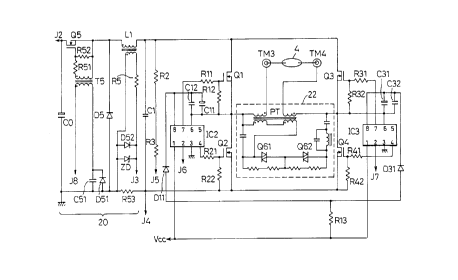
The lighting circuit section shown in FIG. 13 is
provided with a voltage-dropping chopper circuit section
20, which drops the DC voltage at the junction J2 obtained
in the electrolytic capacitor C0 to an optional DC voltage
through a switching element Q5, diode D5 and inductor Ll,
to obtain a lamp voltage at a capacitor Cl, which voltage
at the capacitor Cl is detected through resistors R2 and
R3 and junction J5. Further, the current flowing through
the inductor Ll is detected through a resistor R5 and the
junction J3, and a current flowing to the voltage-dropping
chopper circuit section 20 is detected from an end of a
resistor R53 through the junction J4. The switching
element Q5 in the voltage-dropping chopper circuit 20 is
driven by the drive signal supplied to the junction J8 and
through a transformer T5 and resistors R51 and R52.
Next, a polarity inverting circuit section
comprises a full-bridge circuit of the four switching
elements Ql to Q4 which are respectively driven by means
of general use driving circuits IC2 and IC3 and through
resistors Rll, R12; R21, R22; R31, R32; and R41, R42. The
signals for square wave driving are connected through the
junctions J6 and J7. As an operating source power for the
driving circuits IC2 and IC3, the foregoing constant
voltage Vcc is supplied. Further, capacitors Cll, C12;
and C31, C32 for driving the switching elements Ql and Q3
on higher potential side are charged by this constant
voltage Vcc supplied through a resistor R13 and diodes Dll
and D31. A discharge lamp 4 is connected through a pulse
CA 02206276 1997-0~-27
transformer PT of an igniter circuit 22 to output ends of
the full-bridge circuit, at terminals TM3 and TM4. The
lamp 4 is either M98 (70W) or M130 (35W) of ANSI Standard,
for example, and its light emitting tube is of ceramics.
The igniter circuit 22 stops its pulse generation after
the start of discharge of the lamp 4.
Now, in the present embodiment, the frequency of
the square wave drive signals supplied from the control
circuit 7 of the lighting circuit section through the
junctions J6 and J7 to No. 2 pins of the driving circuits
IC2 and IC3 is set to be low in the non-load state and for
several seconds immediately after the start of discharge,
and the setting is changed over to be high once a stable
lighting state is reached. With the ON width of the
switching element Q5 maintained in a wide state during the
non-load for several seconds immediately after the start
of discharge in which the discharge state is unstable, it
is enabled to prevent the discharge lamp 4 from
extinguishing and to improve the starting characteristic.
It should be appreciated that the start of discharge of
the lamp 4 can be detected in the form of a drop in the
lamp voltage.
EMBODIMENT 7:
In FIG. 14, a circuit arrangement of a seventh
embodiment of the present invention is shown, which
generally comprises a voltage boosting chopper circuit 101
forming a DC power source circuit, a voltage dropping
chopper circuit 102, a polarity inverting circuit 103, and
CA 02206276 1997-0~-27
a control circuit 105 for a drive control of a switching
element Q102 in the voltage dropping chopper circuit 102.
The DC power source circuit 101 is to convert a pulsating
voltage obtained by full-wave rectifying a power from a
commercial AC power source AC by means of the full-wave
rectifier DB into a DC voltage by means of a so-called
voltage boosting chopper circuit 101 comprising an
inductor L101, diode D101, capacitor C101 and such
switching element Q101 as a MOSFET. The voltage dropping
chopper circuit 102 is constituted by such switching
element Q102 as the MOSFET which turns ON and OFF at
several ten kHZ, diode D102 and inductor L102, and a
current IL102 flowing through the inductor L102 is
rendered to be such triangular wave form as shown in FIG.
16(a) and is detected through a resistor R104 connected in
series to a secondary winding of the inductor L102.
Detection output of this current IL102 is provided to the
control circuit 105 and is made to be a feedback signal
for controlling zero-cross switching drive of the
switching element Q102 in the voltage dropping chopper
circuit 102 through the control circuit 105. Further, the
capacitor C102 is to remove a high frequency component
from an output current of the voltage dropping chopper
circuit 102. The polarity inverting circuit 103
constitutes a square wave inverting which converts a DC
output from the former-stage voltage dropping choppr
circuit 102 into a square power of a low frequency and
alternating at several hundred Hz by means of a
- 23 -
CA 02206276 1997-0~-27
full-bridge circuit of such switching elements Q103-Q106
as MOSFET, and supplies a square wave current of a low
frequency to a high pressure discharge lamp LA.
Details of the control circuit 105 for the
drive-control of the switching element Q102 is shown in
FIG. 15, in which the control circuit 15 comprises a zero
current detecting circuit 114 for detecting a secondary
voltage of the inductor L102 in the voltage dropping
chopper circuit 102, a PWM circuit 108 for determining a
signal duty for driving the switching element Q102 of the
voltage dropping chopper circuit 102 and outputting
signals for switching over the switching element Q102 of
the circuit 102, an OFF-time supervising circuit 109 which
outputs a signal in an event when the switching element
Q102 of the circuit 102 is not switched over for more than
a fixed time, a switching circuit 110 for switching over
between the zero current detecting circuit 114 and the
OFF-time supervising circuit 109, and a driver circuit 111
for outputting a driving signal.
In the present embodiment, the switching circuit
110 actuates the OFF-time supervising circuit 109 when the
discharge lamp voltage is below a certain discharge lamp
voltage value Va which is smaller than the largest
discharge lamp voltage (FIG. 17), the current IL102
flowing to the inductor L102 is caused to be sequentially
switched over as in FIG. l9(a), and the lamp can be
prevented from extinguishing while the lamp is maintained
until its stable lighting.
- 24 -
CA 02206276 1997-0~-27
Here, an internal circuit of the OFF-time
supervising circuit 109 is shown in FIG. 18, and this
circuit 109 comprises a variable threshold voltage E101, a
capacitor C103, a comparator CplOl, a constant current
source E102, a resistor R105 for discharging the capacitor
C103 and such switching element Q107 as a transistor. The
threshold voltage E101 will be a voltage which linearly
decreases when the lamp voltage is smaller than the
foregoing lamp voltage value Va but will be a constant
threshold voltage when the lamp voltage is above the value
Va. The relationship between the threshold voltage E101
and the lamp voltage Vla is shown in FIG. 20. When a
charge voltage of the capacitor C103 (FIG. l9(b)) is below
this threshold voltage E101, no driving signal (FIG.
l9(d)) is provided to the switching element Q102 in the
voltage dropping chopper circuit 102. With this OFF-time
supervising circuit 109, the current IL102 flowing to the
inductor L102 can be sequentially switched over as in FIG.
l9(a). As the charge voltage of the capacitor C103
reaches the threshold voltage E101, the comparator CplOl
provides a "High" level signal to the PWM circuit 108. At
this time, a signal "x" for turning the switching element
Q107 ON is provided from the PWM circuit 108 as the
feedback signal, a charge in the capacitor C103 is drawn
out, and the driving signal (the "High" level signal of
FIG. l9(d)) is provided from the driver circuit 111 to the
switching element Q102 of the voltage dropping chopper
circuit 102. The capacitor C103 is kept in short-circuit
- 25 -
CA 02206276 1997-0~-27
state until the output of the PWM circuit 108 becomes the
"Low" level next time.
Next, as the lamp voltage becomes above the
predetermined value Va of FIG. 17, the switching circuit
110 actuates the zero current detecting circuit 114 to
have the current IL102 flowing to the inductor L102
subjected to a discontinuous zero-cross switching, and the
lamp is lighted with a desired lamp power. The zero
current detecting circuit 114 detects a secondary winding
voltage (FIG. 16(b)) of the inductor L101 in the voltage
dropping chopper circuit 102, so that a fall of the
secondary winding voltage of the inductor L102 occurring
when the current IL102 of the inductor L102 in the voltage
dropping chopper circuit 102 becomes zero will be
detected, and a trigger pulse (FIG. 16(c)) is provided to
the PWM circuit 108. Upon receipt of such trigger pulse
from the zero current detecting circuit 114, the PWM
circuit 108 provides a "Low" level signal after
maintaining the "High" level output state for a fixed
time, and this "Low" level signal is transmitted by the
driver circuit 111 to the switching element Q102 of the
voltage dropping chopper circuit 102 as a driving signal
(FIG. 16(d)).
EMBODIMENT 8:
The present eighth embodiment is of the same
circuit arrangement as in the foregoing Embodiment 7 (FIG.
14), and the control circuit 105 corresp~nding to the
switching element Q102 of the voltage dropping chopper
- 26 -
CA 02206276 1997-0~-27
circuit 102 is also of the same arrangement. While in
Embodiment 7 the OFF-time supervising circuit 109 causes
the switching element Q102 to perform the continuous
switching from immediately after the start of lighting of
the discharge lamp and the operation is changed over to
that of the zero current detecting circuit 114 at the
predetermined value Va of the lamp voltage until at least
the discharge lamp power reaches a rated level so that the
switching element Q102 will be switched to cause the
current IL102 flowing to the inductor L102 to perform the
discontinuous switching, the predetermined voltage Va at
which the OFF-time supervising circuit 109 is changed over
to the zero current detecting circuit 104 is set in the
present embodiment to be in range of 30 to 50% of the
rated discharge lamp voltage (when the rated voltage is
90V, for example, the range will be about 25 to 45V) in
which a slow leakage as one of lamp accident modes occurs
(a phenomenon in which the lamp voltage is lowered by the
leakage of gas in the light emitting tube and an excess
current is caused to be kept flowing to the lamp).
EMBODIMENT 9:
FIG. 21 shows a circuit arrangement of
Embodiment 9 of the present invention, in which a
discharge lamp voltage detecting circuit 104 is added to
the circuit of FIG. 14, while the control circuit 105 has
such arrangement as shown in FIG. 22. The discharge lamp
voltage detecting circuit 104 detects the lamp voltage of
the high pressure discharge lamp LA by means of a series
CA 02206276 1997-0~-27
circuit of resistors R101 and R102 connected in parallel
with the source power input ends of the polarity inverting
circuit 103, and thus detected lamp voltage VlalOl is
provided to the control circuit 105 as a feedback signal
for the drive-control of the switching element Q102 of the
voltage dropping chopper circuit 102 through the control
circuit 105. With the provision of this discharge lamp
voltage detecting circuit 104, the OFF-time supervising
circuit 109 is changed over to the zero current detecting
circuit 114 once the lamp voltage has reached the
predetermined value Va, and the value of the lamp voltage
is made to correspond to the ON width ton (ON duty) of the
switching element Q102 of the voltage dropping chopper
circuit 102 (FIG. 23).
In the control circuit 105, an inverting circuit
106 for inverting the detected value of the lamp voltage
as well as a discriminating circuit 107 for comparing the
detected value of the lamp voltage with its inverted value
to utilize a lower one of these values, are additionally
provided. In FIG. 24, a solid line represents the
detected value VlalOl obtained by voltage-dividing the
lamp voltage, and a dotted line represents the inverted
value VlalO2 of the detected value VlalOl of the lamp
voltage. This dotted line may be varied in the gradient.
The discriminating circuit 107 selects the lower one of
the detected value VlalOl and the inverted value VlalO2,
and the selected lower value is output to th-e PWM circuit
108. This lamp voltage obtained through the comparison
- 28 -
CA 02206276 1997-0~-27
will be a threshold voltage of the PWM circuit 108, and
the ON width ton (ON duty) of the switching element Q102
of the voltage dropping chopper circuit 102 is determined
as shown in FIG. 23. With such provision of the discharge
lamp voltage detecting circuit 104, the OFF-time
supervising circuit 109 can be changed over to the zero
current detecting circuit 114 when the lamp voltage
reaches the predetermined value Va and, after the change
over, the ON width of the switching element Q102 of the
voltage dropping chopper circuit 102 can be controlled in
accordance with the value of the lamp voltage.
EMBODIMENT 10:
In FIG. 25, a circuit arrangement of Embodiment
10 according to the present invention is shown, in which a
discharge lamp current detecting circuit 112 is added so
that, as the discharge lamp current value is detected to
have reached a predetermined value, the OFF-time
supervising circuit 109 is changed over to the zero
current detecting circuit 114. Further, the control
circuit 105 here is arranged as shown in FIG. 26. The
discharge lamp current detecting circuit 112 detects the
lamp current of the high pressure discharge lamp LA by
means of a resistor R103 connected in series with the
source power input end of the polarity inverting circuit
103, and thus detected value IlalOl is provided to the
control circuit 105, in which the switching circuit 110
changes the OFF-time supervising circuit 109 over to the
zero current detecting circuit 114. Other respects in the
- 29 -
CA 02206276 1997-0~-27
circuit arrangement are the same as those in Embodiment 9
and their description shall be omitted here.
EMBODIMENT 11:
FIG. 27 shows a circuit arrangement of the
control circuit 105 in Embodiment 11 of the present
invention. While the main circuit arrangement of this
embodiment is the same as that in FIG. 25, the control
circuit 105 is different in an additional provision of a
timer circuit 113. When the lamp current is detected by
the discharge lamp current detecting circuit 104, the
timer circuit 113 starts an integration of time. Since
the time from the start to a rated discharge lamp voltage
reached is substantially fixed, the time constant of the
timer circuit 113 is made to be in conformity to the time
until the predetermined value Va of the lamp voltage is
reached. When this time for reaching the value Va is
over, the switching circuit 110 changes the OFF-time
supervising circuit 109 over to the zero current detecting
circuit 114.
EMBODIMENT 12:
FIG. 17 is also an explanatory view for
Embodiment 12, wherein a duty width of ON signal provided
from the driver circuit 111 in a low lamp voltage range in
which a damage due to such multicurrent as the slow
leakage in Embodiment 7 is likely to occur is set to be
narrow, so that the circuit characteristic of less lamp
current in the low lamp voltage range can be- obtained, as
shown in FIG. 17.
- 30 -
CA 02206276 1997-0~-27
EMBODIMENT 13:
Similarly, in Embodiment 8, the risk due to the
multicurrent at the time of slow leakage can be reliably
eliminated as shown in FIG. 17, by setting to be smaller
than usual the ON width of the driving signal output from
the driver circuit 111 under the control of the zero
current detecting circuit 114 to which the operation has
been changed over at the predetermined lamp voltage value
Va in the abnormal state of the lamp including the slow
leakage.
In FIG. 28, a circuit characteristic relying
only on such ON width control as shown in FIG. 23 in which
the OFF-time supervising circuit 109 is not operated, is
shown as a comparative example. In the present
embodiment, the zero current detecting circuit 114 and
OFF-time supervising circuit 109 are changed over at the
predetermined value Va in the low voltage range in which
the slow leakage is likely to occur, and the ON width of
the driving signal is set to be smaller in the low voltage
range.
While in the foregoing embodiments the discharge
lamp lighting device has been referred to only partly and
details of the whole circuit arrangement have not been
described, an example of their application to a practical
discharge lamp lighting device will be as in the
followings.
EMBODIMENT 14: -
An example of the discharge lamp lighting device
CA 02206276 1997-0~-27
embodying the present invention as a practical product is
shown in FIGS. 29-31, in which FIG. 29 shows a source
power input section, FIG. 30 shows a power factor
improving section, and FIG. 31 shows a lighting circuit
section, the respective sections being mutually connected
at junctions J101-J108.
In the source power input section of FIG. 29,
the AC power source AC is connected to terminals TMl and
TM2 of the device and, through a fuse FS, thermal
protector TP, low resistor R100 and a filter circuit, to
AC input terminals of the rectifying circuit DB to the DC
output terminals of which a capacitor C109 is connected.
This capacitor C109 is of a small capacity, and the actual
smoothing is performed at a voltage boosting chopper
circuit in the later staged power factor improving
section. The filter circuit includes a zinc oxide
non-linear resistor ZNR for absorbing any surge voltage,
coils L105 and L106 and capacitors Cx, Cy, C108, C181 and
C182, and a junction in a series circuit of the capacitors
C181 and C182 is connected through a further capacitor
C183 to an earthing terminal TM105.
The power factor improving section as shown in
FIG. 30 comprises a voltage boosting chopper circuit
including an inductor L101, a switching element Q101 and a
diode D107, a full-wave rectified output of the rectifying
circuit DB is received at the junction J101, and a boosted
and smoothed DC voltage is obtained at an-electrolytic
capacitor C101 (FIG. 31) connected to the junction J102.
- 32 -
CA 02206276 1997-0~-27
The switching element Q101 of the voltage boosting chopper
circuit is driven by the driving signal provided from the
voltage boosting chopper controlling circuit 115 through
resistors R171 and R172, and the current of this signal is
detected by a resistor R173. A current flowing through
the inductor L101 is detected by a resistor R174 connected
to a secondary winding of the inductor L101. An output
voltage generated at the junction 102 is detected through
resistors R108 and R109, and an input voltage at the
junction J101 is detected through resistors Rl91 and R192.
An operating source power VcclOl is supplied from the
junction J101 through resistors R193 and R194 upon
connection of the power source, whereas, as the switching
operation of the switching element Q101 starts, a
secondary winding output of the inductor L101 is rectified
at diodes D171 and D172, and a DC voltage obtained at a
capacitor C171 through a resistor R170 is supplied through
a diode D173. This DC voltage obtained at the capacitor
C171 is made to be a constant voltage by means of a
three-terminal type voltage regulator IC101, so as to be
an operating source power Vcc of the control circuit 116
for the lighting circuit section. This control circuit
116 detects through junctions J103-J105 the zero current,
excess current and lamp voltage from the lighting circuit
section of FIG. 31 and provides square wave driving
signals and voltage dropping chopper driving signal
through junctions J106-J108.
The lighting circuit section shown in FIG. 31
CA 02206276 1997-0~-27
which drops the DC voltage obtained at the electrolytic
capacitor C101 through the junction J102 to an optional DC
voltage by means of an action of a switching element Q102,
diode D102 and inductor L102, and a lamp voltage is
obtained at a capacitor C102. The lamp voltage at the
capacitor C102 is detected through resistors R102 and R103
and junction J105. A current flowing through an inductor
L102 is detected through a resistor R104 and junction
J103, and a current flowing through the voltage dropping
chopper circuit section 102 is detected through the
resistor R103 and junction J104. The switching element
Q102 of the voltage dropping chopper circuit section 102
is driven, through a transformer T105 and resistors R151
and R152, by the driving signal supplied to the junction
J108.
Next, the polarity inverting circuit section is
a full bridge circuit of four switching elements Q103-Q106
which are driven respectively by means of general-use
drive circuits IC102 and IC103 and through resistors Rlll,
R112; R121, R122; R131, R132; and R141, R142. The square
wave driving signals are connected through the junctions
J106 and J107, and the foregoing constant voltage Vcc is
supplied as the operating source power of the respective
drive circuits IC102 and IC103. Further, capacitors Clll,
C112; C131, C132 for driving the switching elements Q103
and Q104 on the higher potential side are charged with the
constant voltage Vcc through a resistor R11-3 and diodes
D111 and D131. To output ends of the full bridge circuit,
- 34 -
CA 02206276 1997-0~-27
Dlll and D131. To output ends of the full bridge circuit,
a discharge lamp LA iS connected through a pulse
transformer PT of an igniter circuit 117. The discharge
lamp LA iS of M98 (70W) or M130 (35W) of ANSI Standard,
for example, and its light emitting tube is of ceramics.
The lamp LA is connected across terminals TM103 and TM104
of the pulse transformer PT.