Note: Descriptions are shown in the official language in which they were submitted.
~ t CA 02206322 1997-05-28
r~ L~IC~
Description
Method for reducing jitter of ATM cells
The invention relates to a method according to
the preamble of patent claim 1.
In ATM cn----lln; cations networks, information i8
transmitted in the form of packets or cells according to
an asynchronous transmission mode (Asynchronou~ Transfer
Mode, ATM). In these ATM networks, jitter of the ATM
cells occurs, dictated by the system, during the
transmission operation. Jitter i5 generally produced by
buffering of the ATM cells, which is carried out in a
network node, and depends on a number of parameters.
Thus, for example, the n~her of nodes in the network,
the lo~; ng (that i~ to say how many bits/s are trans-
mitted) and the nature o$ the traffic (that i~ to ~ay
whether a variable bit rate i~ transmitted) have a direct
influence on the jitter magnitude. The jitter of an ATM
cell thus fluctuates between 0 (optimum value, in other
word~ no jitter) and a maY;ml~m ~alue. The occurrence of
jitter is particularly disadvantageous when the trans-
mitted information takes the form of video signals or
voice signals.
Limit values have been specified in the past for
the purpose of avoiding excessively high jitter. Thus,
for example in accordance with a specification made by
the Federal German Post Office, the maximum jitter per
network node must not exceed a value of 250 ~8. In the
case of a connection in which 6 network nodes are tra-
versed (typical value for a national connection), the
maximum jitter can consequently amount to up to 1.5 ms.
If a transmission bit rate of 4 Mbit/s (correspon~; n~ to
a rate of 10000 cells/s) i3 taken as a basis, this mean3
that, in the extreme case, instead of 15 ATM cells, not
a single ATM cell arrive~ in the receiving device.
CA 02206322 1997-05-28
- 2 -
German Patent Specification DE 41 32 51Q C2
discloses a circuit arrangement for the transmission of
digital message signals via a broadband communication~
system operating according to the asynchronous transfer
mode. Said document di~clo8e~ how the effects of jitter
in a receiving device can be reduced. This i8 done by
self-synchronization o~ bu~fer ly devices, which
proves to be complicated in practice.-
The invention is based on the ob;ect of specify-
ing a method which enables the e~foct~ o~ jitter to bereduced further using relatively 8imple msans.
Th~ invention is achieved, based on the preamble
of patent claim 1, by means of the features specified in
the characterizing part.
The invention has the advantage that the inter~al
between two succes8ive ATM cell~ ie determined prior to
~torage in the memory device of tha receiving device. The
interval~ determined in thi~ way are then ~ ' over a
fixedly defined plurality of ATM Cell8 and averaging iQ
carried out on the b~sis of the~e calculation~. The
average value calculated in this way i~ then u~ed to read
the ATM cells ~tored in the memory device back out of the
memory device and forward them. This i~ associated with
the advantage that the jitter is reduced.
Advantageous refinements are specified in the
~ubclaims:
According to claim 2, it is provided that the
averaging of the intervalQ between the in each case two
3uccessive ATM cells is carried out anew each time an ATM
cell arrives.
CA 02206322 1997-05-28
According to claim 3, it i~ provided that the
averaging is carried out in that the last calculated
average value of the ~um of the interval~ b~tween the
defined number of ATN cells is subtracted from the la_t
calculated sum o$ the intervals between the defined
number of ATM cell~, and the newly dete ;ne~ interval of
the ATM cell that arrived last i_ add~d. This is associ-
ated with the advantage that the respect~ve counter
re~n~s do not have to be buffered.
According to claim 4, it is provided that a
correction quantity i8 added to and/or subtracted from
the averaging result wh~never the occupancy of the memory
device deviates from a defined ~alue, and that the ATN
cellQ ~tored in the at lea~t one memory devico are read
out using the value determined in thi~ way. Thi~ i8
a~sociated with the advantage that the rO~n~n~J errOr8
which occur unavoidably during the calculation of the
average value can at lea~t partially be compen~ated for
again. In particular, the correction quantity can be used
whenever deviation~ from the optimum occupancy of the
memory de~ice occur.
According to claim 5, it i~ provided that the
initial ~tate i~ produced in that the at lea~t one memory
device i~ first of all only half-filled with ATM cells,
the intervals are su~med and the value determined in this
way is extrapolated to the number of ATM cells over which
averaging i_ carried out. Thi~ i8 asEIociated with the
advantage that the averaging iR only carried out whenever
staDie condi~ion~ aru acnieved.
According to claim 6, it iR provided that the
interval between two ~ucce~sive ATM cell~ is dete ;ne~
by counting the clock pulses of a clock pul_e train
g~nerated by a counting register provided on the input
~ide of the at least one memory device, the clock rate of
said clock pulRe train being very much
- CA 02206322 1997-05-28
L - 4 -
higher than the transmis~ion rate at which the ATM cQlls
are transmitted from the transmitting device to the
receiving device. This i8 associated with the advantage
that the error in the determination of the interval can
be kept small.
According to claim 7, it i~ provided that the
fixedly defined plurality of ATM cells over which averag-
ing i8 calculated -i~ a power of 2. This i~ a~EIociated
with the advantage that the calculations can be carried
out by hardware with little outlay.
According to claim 8, it is provided that the ATM
cells are read out from the at least one memory devic~ by
10A~; ng a counting register, which i~ arranged on the
output side of said memory device, with the av~rage value
to which the correction quantity has been applied. This
i~ associated with the advantage that the ATM cells are
read out at the average value of the jitter that ha~
occurred.
According to claim 9, it is provided that the
following i~ applicable to the dimensioning of the at
least one memory device:
FIFO=2 . m~x~mum b~trate m~xfmum .1~tter
the var~h~ FIF0 has the dimension n cells~. Thi~
i~ associated with the advantage that the memory device
can be optimally adapted in terms of its storage capac-
ity.
The invention is expl~; neA in more detail belowusing an exemplary embo~; - t with reference to a figure.
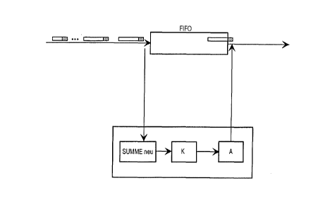
The figure shows a memory device FIF0. Thi~ i8
expediently a memory device which readA incoming ATM
cells in and out again according to the "first-in/first-
out" principle. It is expedient to provide just a memory
device FIF0 having a small dimensioning. According to the
fi~ure, the ATM cell~
CA 02206322 1997-05-28
output by a transmitting device arrive at the left of the
memory device FIFO and are written thereto.
According to the invention, before the ATM cell8
are written to the memory device FIFO, the interval with
re~pect to the preceding ATM cell is det~ ;ne~. This iB
done with the aid of a counting device, which is not
shown in the figure and i~ provided on the input side of
the memory device FIFO. It should be taken into account
here that the clock rate at which the counting device
determines the interval i~ very much greater than the
tran~mission rate of the ATM cells. The aim of the
procedure according to the in~ention i~ to determine an
average r~ception data rate A. A particularly simple
realization i8 provided when the number of ATM cell~ over
which averaging is carried out is a power of 2. In his
case, the averaging can then be carried out by means of
a simple ~hift operation. For example, a value can be
divided by 256 by shift~ng this value to the right by
ld 256 = 8 bit~, where ld 256 represent~ the logarithm to
the base two of 256.
The reception data rate is determ;ne~ by buf er-
ing the counter re~ing of the counting device when an
ATM cell arrive~, and era~ing the count~r again. Thi~
counter reA~; ng is then incorporated into th~ previously
determined average value in that the current average
value i~ firstly ~ubtracted from the ~um of the interval~
between the last N ATM cQlls, and the counter reA~;n~ of
the newly arrived Al~ CQll i8 added to thi~3 ~uantity.
These operation~ are repre~ented by the formula
~us~eumbld - (average value of ~umOld) I counter
r~; n~ .
- CA 02206322 1997-0~-28
After an ATM cell has been read out from the
memory device FIFO, on the output ~ide a further counting
device, which i8 likewise not shown in the figure, i~
loaded with the currently determined average value, to
which a correction quantity }C, which i8 to be explained
later, is applied. This counting devica then reduce~ the
loaded value at the ~amQ clock rate as the counting
~ device on the input side. Once the value of the counting
de~ice has r~rhe~ zero, the ATM cell i~ read out from
the memory device FIFO.
However, the shift operation when calculating ths
average value results in a rol~n~; ng error. In practice,
therefore, during the calculation of the average value,
rolln~ n~ down of this value is performed. If this average
value alone were taken as a basis for the read-out
operations, this would mean that the ATM cells would be
read out from the memory d~vice FIFO too quickly. For
th$s reason, a correction guant$ty ~ i8 provided, by
means of which the rolln~; ng error that has occurred i9
corrected again. This correction ~uantity R is applied to
the formula spec$f$ed above. In practice, this means that
the read-out operationQ are now dependent on the occu-
pancy of the memory device. For example, the average
value calculated is rounded up whenever the memory device
FIFO is less than half-filled. Co ve~ely, it i~ rounded
down ~never the memory device FIFO is more than half-
filled. However, it should be taken into account that the
optimu~ occupancy depends on the statistical di~tribution
of the jitter values; this means that this optimum
occupancy does not necessarily have to be achieved at the
half-filled level.
The procedure which has ~ust been described is
expedient particularly when a stable state has already
been reached and an initial state, howsoever defined, has
been left behind. In this respect, it is necessary to
Qstablish this initial state at the beg;nn;ng of a
transmission of ATM cQlls. For this reason, at the
beg; nn; ~g of the data transmission, the memory device
FIFO
~ CA 02206322 1997-05-28
i~ half-filled with ATM cells. The counting device on the
input side then sums the counter re~ g8 on the arrival
of the ATM cells. The summation value determined in this
way is then extrapolated to the sum of N ATM cells.
Expediently, the occupancy should likewise be a power of
2. What thi~ achieve~, in a simple manner, is that this
extrapolation i8 simple to carry out by means of an
operation shifting the sum to the left. In this initial
phase, it should be taken into account that the average
value here is ~till relatively far ~ vad from the
actual average value. In thi8 respect, a greater depend-
ence of the average value on the occupancy of the memory
device FIF0 may occur at this time. If, howeve , the
initial state ha~ become ~table as a result of the
procedure de~cribed abovo, the method according to the
invention take place according to the principle descr~bed
above.
Finally, the dimensioning of the memory device
FIF0 will also be discussed:
As already mentioned, the ~itter distribution
depends on the cell rate of the ATM cells, since the ATM
cells cannot overtake one another. It i8 admittedly
possible for the ~itter of the interval between one cell
and the following ATM cell to shoot up from 0 to a
maximum value; conversely, however, jitter can drop by no
more than one cell cycle, since otherwise cell~ would
overtake one another. For this reason, the memory device
FIF0 must be dimensioned in ~uch a way that as many ATM
cells can fail to appear as is the ca~e when the ~itter
jumpe in one go from zero to the maximum value.
Consequently, the following formula can be specified for
the dimensioning of tho memory device FIF0:
FIrO=2 . m~r~mum bltrate ~ m~xlmum ,~ltter
bl t~/cell
CA 02206322 1997-05-28
- 8 -
In principle, in this procedure, cell lo~es and
incorrectly routed cells can only be identified during
cell cycle time~ which are considerably longer than the
-Y~ jitter. This would be the ca~e, for example, for
5a cell cycle time of 64 lcbit/~ ~ 170 cell~/s = 6 ms cell
cycle very much greater than 1.5 m~ jitter. After the
~ettling process, it is possible to ~pecify a time window
during which an ATM cell mù~t arrive. If an ATM cell doe~
not arrive during this time w~ndow, then, by definition,
the ATM cell is lost. If an ATM cell arrives out~ide this
time window, it cannot then belong to the relevant
connection.