Note: Descriptions are shown in the official language in which they were submitted.
CA 02206416 2005-O1-14
24005-207
1
Array of radiating elements
The invention relates to an array of radiating
elements to be used as a module in a phased array radar
antenna, the radiating element being shaped like a waveguide
enclosed by walls, which waveguide is substantially
rectangular in cross-section.
Such an array is known from the European patent
application EP-A- 0.554.378. This patent application
describes an antenna module for an active monopulse phased-
array system comprising a housing incorporating four
radiating elements shaped like waveguides of rectangular
section. By suitably stacking the antenna modules, a
substantially continuous antenna surface is obtained.
The array according to the invention has for its
object to effect an improvement on said patent application
as regards rigidity and distortion. A further object is to
provide an array that can be manufactured easier and at
relatively lower cost.
According to the invention there is provided
linear array of rectangular waveguide radiating elements, to
be used as a module in a two-dimensional phased array
antenna, characterized in that the linear array of
rectangular waveguide radiating elements comprises a common
surface and at least one row of discrete at least over a
certain length U-shaped sections each of which has two
parallel walls having free ends, the U-shaped sections being
mounted substantially parallel to each other and to the
CA 02206416 2005-O1-14
24005-207
la
common surface with the ends of their parallel walls
connected to the common surface over the length that they
are U-shaped.
A favourable embodiment of the array is
characterized in that the surface constitutes the widest
side wall of each radiating element.
If the radiating elements have a non-square
section, which generally is the case, these elements can be
best mounted on the surface such that the widest wall of
these elements faces the surface, as a result of which the
surface constitutes the widest wall of each radiating
element. Thus, maximum benefit may be derived from the fact
that the
CA 02206416 1997-OS-29
WO 96/20515 PCT/EP95/05146
2
surface can constitute a side wall of a radiating element,
which saves material cost and ensures a rigid construction.
A further favourable embodiment of the array is
characterised in that the surface comprises a sheet-shaped
element. Such elements are inexpensive and easy to
manufacture and moreover offer good attachment
possibilities.
A further favourable embodiment of the array is
characterised in that at least a part of a radiating
element comprises a channel section, which is mounted to
the surface by the base parts of both vertical channel
section side walls.
This entails a considerable number of advantages. Firstly,
channel sections are easy to manufacture and particularly
easier than tubular ones. The first type of sections can
usually be obtained through a rolling process, whereas the
latter are generally obtained on the basis of the far more
expensive extrusion process. Channel sections can
furthermore be easily secured to a surface by for instance
soldering the vertical side walls to it, without causing
additional gaps or cavities that could adversely affect the
electrical properties of the antenna. Also from a
mechanical point of view, the use of channel sections
secured to a surface in said manner is to be preferred to
the use of tubular sections. By building up the radiating
elements from channel sections mounted against the surface,
benefit may simultaneously be derived from the fact that
the surface can serve as radiating element side wall. The
channel section will then have to be mounted to the surface
throughout the entire length of the side wall without any
air gaps.
CA 02206416 1997-OS-29
WO 96/20515 PCT/EP95/05146
3
It is also possible to provide slots in the surface over
the entire length of the channel section to accommodate the
vertical side walls of the channel section. This
particularly facilitates manufacturing. The channel
sections can be fit in the slots and can subsequently be
secured by soldering without moving out of position.
A further favourable embodiment of the array is
characterised in that, for at least one radiating element,
at least in assembled state, a transformer element is
provided for feeding, at least substantially reflection-
free, radiant energy into said radiating element.
Such a transformer element renders it possible to create,
at only extremely low losses, a coupling of radiant energy,
generated by an externally-positioned transmitter. In view
of the radiating elements being closely spaced, there is
hardly or no room left at the side of the radiating element
to allow the coupling of radiant energy. It will
2o consequently be required to introduce the radiant energy at
the back of the radiating element, for which purpose a
transformer element is eminently suitable.
A further favourable embodiment of the array is
characterised in that at least one transformer element, at
least in assembled state, is integral with the surface.
This entails specific advantages, particularly in the
manufacture of the array. The surface, for instance a
sheet-shaped surface, can first be provided with the
transformer elements, for instance through soldering, after
which the radiating elements can be provided in a
subsequent operation.
CA 02206416 1997-OS-29
WO 96/20515 PCT/EP95/05146
4
A further exceptionally favourable embodiment of the array
is characterised in that the at least one transformer
element is manufactured such that it is integral with the
surf ace .
If the positioning of separate transformer elements is a
time-consuming operation, which is generally the case, it
is recommendable to manufacture the transformer elements
such that they are integral with the surface. This saves a
substantial number of operations, resulting in an overall
reduction of manufacturing costs. When using channel
sections as component parts of the radiating elements in
combination with transformers, material will have to be
removed where the surface exhibits a bulge owing to the
presence of a transformer element. The channel section will
then as it were cover the transformer element. The combined
use of channel sections and transformer elements which are
manufactured in one process with the surface particularly
offers the advantages of a simple manufacturing process in
combination with a light-weight construction having a high
degree of rigidity. When using tubular sections, the
placement of a transformer element per radiator is
considerably more time-consuming than would be the case
with channel sections realised in said manner.
A further favourable embodiment of the array is
characterised in that the surface has been manufactured in
combination with the at least one transformer element in at
least one extrusion operation, in the course of which the V
cross-sectional shape of the at least one transformer
element is revealed for the first time.
Based on a sheet-shaped basic section, it is possible to
manufacture the sheet-shaped surface pertaining to the
array, completely provided with the sheet-shaped basic
CA 02206416 1997-OS-29
WO 96/20515 PCT/EP95/05146
section of all transformer elements in one extrusion
operation. By subsequent mechanical operations, such as
milling, drilling or broaching, further details required
for the proper functioning of a transformer element can be
5 provided. A further advantage of the surface thus
manufactured is that there is a high-strength connection
between the transformer elements and the surface is very
strong.
A further favourable embodiment of the array is
characterised in that a transformer comprises a
substantially sheet-shaped conductor, disposed
substantially parallel to the surface, which conductor is
at a certain point connected with the surface and for the
rest encloses a gap-shaped cavity between itself and the
surface. Such transformers possess suitable electrical
properties and are pre-eminently suitable to be realized by
extrusion, particularly in combination with the surface.
Additionally, the sheet-shaped surface can at one end be
provided with a connector for attaching a radiant energy
transmission line. This enables each radiating element to
be individually controlled via each individual transmission
line.
A further favourable embodiment of the array is
characterised in that radiation elements are disposed on
both sides of the surface. Thus, full benefit can be
derived from the fact that a surface has two sides and
consequently enables a maximum number of radiating elements
to be applied per array. This results in a lighter and more
compact construction, since fewer surfaces are required for
the complete antenna.
CA 02206416 1997-OS-29
WO 96/20515 PCT/EP95/05146
6
A further favourable embodiment of the array is
characterised in that a row of radiation elements
positioned on one side of the surface is staggered
relatively to a row of radiating elements positioned on the
other side of the surface. This yields a more rigid
construction at a constant weight and has the added
advantage that the beam formation is considerably improved.
A further favourable embodiment of the array is
characterised in that a row of radiating elements on one
side of the surface is staggered relatively to a row of
radiating elements positioned on the other side of the
surface over a distance that is substantially equal to half
the distance between the centre lines of two radiating
elements at one side of the surface. This yields an optimal
rigidity and an optimal configuration as regards the beam
formation properties.
It is subsequently possible to contiguously position
several arrays according to the invention, such that a
substantially continuous antenna surface is obtained. A so-
called iris plate may be mounted at the front side of this
surface, which on the one hand strongly reduces the mutual
interference of the various antenna modules and on the
other hand greatly improves the rigidity of the
construction. The iris plate may consist of a plate having
conductive properties, which, at the position of the
radiating elements, has been provided with holes that shall
preferably be rectangular in shape with a smaller surface
than the radiating element apertures. Subsequently, a back
plate can be placed at the back which, at the position of
the transformers, is provided with connectors, a connector
fitting a connector connected to a transformer. The back
plate additionally improves the rigidity of the
construction.
CA 02206416 1997-OS-29
WO 96/20515 PCT/EP95/05146
7
The array
according
to the invention
will now
be explained
in greater
detail with
reference
to the following
figures,
of which
Fig. lA represents an array of radiating elements
according to the invention, comprising a surface
designed as a sheet-shaped element on both sides
of which the radiating elements are disposed;
Fig. 1B represents the cross-section A-A, as presented in
Flg. lA;
to Fig. 2 represents a number of arrays of radiating
elements according to the invention, which have
been placed side by side and in which an iris
plate and a back plate have been provided;
Fig. 3 represents a channel section to be incorporated in
an array of radiating elements according to the
invention;
Fig. 4 represents a sheet-shaped element to be
incorporated in an array of radiating elements
according to the invention.
An active monopulse phased-array radar is basically
composed of a plurality of antenna modules. Each antenna
module will be provided with a radiating element and all
radiating elements combined will constitute the antenna
surface. A well-considered design of the module will be
essential to obtain a satisfactory price-performance ratio.
An active monopulse phased-array radar additionally
comprises means to which the antenna modules can be
mounted. A distribution network shall also be provided for
a power supply purposes and for RF transmission signals.
Furthermore, summation circuits and difference circuits
shall be provided for the generation of E, 08 and of output
signals.
CA 02206416 1997-OS-29
WO 96/20515 PCTIEP95/05146
8
As it will generally have to be mounted at the top of a
ship's mast, a radar antenna shall preferably be light-
weight. A light construction will mostly also be more
inexpensive than a heavier construction. When using metal
waveguides as radiating elements in a phased-array radar
antenna, an economical use of materials is consequently
essential.
A phased array radar antenna comprises a plurality of
radiating elements. It is therefore recommendable to keep
the number of components per radiating element as
restricted as possible. With a view to manufacturing, it is
advisable to aim at a non-complex design of the components
required per radiating element. The design of the
components shall preferably be such that a large number of
components can be realised in a limited number of
manufacturing operations.
Also with a view to assembly, a restricted number of
components is preferred. The design of the antenna shall
enable a large number of components to be mounted in a
limited number of assembly operations.
To enable the beam form to be accurately defined, it is of
importance that the radiating elements are positioned
accurately and at equal relative distances. The positioning
of the radiating elements shall additionally be highly
independent of external forces. This consequently requires
a rigid construction. _.
The array of radiating elements according to the invention
to be used as module in a phased array antenna has for its
object to meet all said requirements.
CA 02206416 2005-O1-14
24005-207
9
Fig. lA represents the back part of an array of
radiating elements 1 according to the invention, comprising
a surface designed as a sheet-shaped element 2 to both sides
of which the radiating elements are mounted. The back is
the side at which radiant energy from a T/R element, not
shown here, can be fed into the associated radiating
element. The radiating elements consist of channel or U-
shaped sections 3, provided with three side walls comprising
a web plate 4 and two vertical side walls 5. Via the base
part 6, the vertical side walls 5 are connected to the
surface 2. In this way, the surface 2 constitutes a fourth
side wall of all radiating elements. The radiating elements
are disposed at least substantially in parallel on the
surface 2. If required, the radiating elements may at the
front side be extended beyond the sheet-shaped element 2.
By mounting channel-shaped elements to a plate, the
construction is less likely to be deformed which enables the
beam formation process to be more accurately defined.
Benefit can moreover be derived from the fact that the
surface 2 is capable of constituting a radiating element
side wall. To this end, the surface shall have conducting
properties. An additional advantage is that the surface
also functions as a mechanical connection between the
radiating elements.
The connection between the channel sections and
the sheet-shaped element 2 preferably comprises a soldered
joint that at least substantially covers the entire length
of the base part 6. In the embodiment in question, the
vertical side walls 5 are shorter than web plate 4. The
CA 02206416 2005-O1-14
24005-207
9a
width of web plate 4 shall be greater than ~/2 to prevent
the radiating element from entering the cutoff mode. In the
illustrated embodiment, the sheet-shaped element 2 thus
constitutes the widest side wall per radiating element,
although this might also be the narrow side wall.
Transformer elements 7 are mounted on surface 2.
CA 02206416 1997-OS-29
WO 96/20515 PCT/EP95/05146
Fig. 1B represents cross-section A-A as indicated in Fig.
lA. This figure shows that the transformer elements 7
comprise a sheet-shaped part 8, which together with sheet-
shaped surface 2 envelops a slot 9. Via intermediate part
5 10, the sheet-shaped part 8 is electrically and
mechanically connected to surface 2. The sheet-shaped part
8 is furthermore provided with a connector shaped as a hole
il that matches a transmission line shaped as a pin 12, via
which high-frequency energy can be applied to the
10 transformer element 7. The transformer element 7 allows for
a reflection-free coupling into the radiating element 1 to
transmit the radiant energy.
Fig. 1B furthermore shows a back plane 13. The back plane
13 is provided with conducting pins 12, which match the
holes il in the sheet-shaped parts 8 of the transformer
elements and which are on the other side connected to a T/R
module. The back plane 13 may on a level with the pins 12
be provided with short protruding parts, not shown in the
figure, which accurately fit a radiating element. In this
manner, an array of radiating elements can be fixed to the
back plane prior to final assembly.
In the illustrated embodiment, the transformer elements 7
are manufactured such that they are integral with the
sheet-shaped surface 2. The transformer elements can for
instance be realised in an extrusion process which after
one operation already reveals the profile of the
transformer elements 7. Subsequently, material may be
removed in milling operations at the places of attachment
of the base parts 6 of the channel sections to the sheet-
shaped surface 2. This may be effected such that the
intermediate part l0 has the same width as the inside of
web plate 4 of a channel section, so that the channel
sections can be secured by soldering without moving out of
CA 02206416 1997-OS-29
WO 96/20515 PCT/EP95/05146
11
position. It is also possible for the intermediate part l0
to be narrower than the inside of web plate 4 and to
provide slots, by for instance milling, in the surface 2 at
the location of the base parts 6 of the channel sections
into which the channel sections accurately fit. It will be
obvious that the options for the pre-fixation of the
channel sections are not restricted to those discussed
above but also many other possibilities exist, such as the
use of detachable spacing jigs. For the sake of clarity,
none of the available options have been indicated in the
figure. Providing slots is the preferred option as it is a
time-saving and effective pre-fixation method.
The transformer elements can also be manufactured by
machining the transformer element contours out of a thicker
plate.
The channel sections and the sheet-shaped surface combined
with the transformers are preferably made of the same
material type, for instance aluminium.
In positioning radiating elements on both sides of the
sheet-shaped surface, it is advantageous to stagger the
radiating elements on one side of the surface with respect
to the radiating elements on the other side of the surface
over a distance, marked a2 in Fig. lA, which is
substantially equal to half the distance, marked al in Fig.
lA, between the centre lines of two radiating elements.
This is convenient both with respect to the antenna pattern
to be realised and with respect to the mechanical rigidity
of the array of radiating elements.
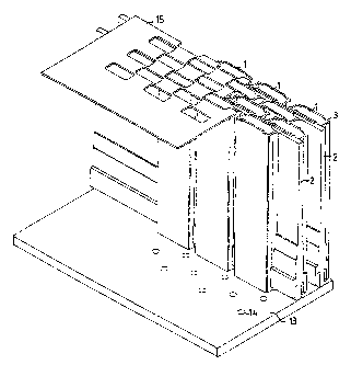
Fig. 2 indicates how a number of array of radiating
elements 1 according to the invention can be assembled to
obtain an antenna surface extending in two directions. At
CA 02206416 1997-OS-29
WO 96/20515 PCT/EP95/05146
12
the back, the arrays are mounted on a back plane 13, which
is provided with holes 14 for the feed-through of
transmission lines not indicated in the figure, which
transmission lines can be connected to their respective
transformer elements 7, which are not exposed to view in
the figure owing to the presence of the channel sections.
The channel sections 3 are disposed on both sides of the
sheet-shaped surfaces 2. An iris plate 15 has been mounted
at the front of the radiating elements. This plate reduces
the mutual interference of the various radiating elements
and to a greater extent provides mechanical rigidity. The
holes in the iris plate are smaller than the surface at the
aperture of a radiating element. The iris plate can be
secured by means of a soldered connection.
Fig. 3 represents a channel section 3, which may serve as
radiating element in the array according to the invention.
The numbering of the separate parts corresponds to the
numbering in the preceding figures. The channel section can
for instance be manufactured in a rolling or extrusion
process. At the position of the base parts 6 of channel
section 3, the side wall is thickened to some extent, which
facilitates the mounting of the channel section.
Fig. 4 represents a surface 2 designed as a sheet-shaped
element, which comprises a number of transformers 7. The
numbering of the separate parts again corresponds to the
numbering in the preceding figures. The transformers 7 are
manufactured as integral parts of the sheet-shaped element
through extrusion of the sheet-shaped element, which yields
an elongated profile of the transformers. At the places of
attachment of the base parts 6 of the channel-shaped
elements, strips have been removed by milling at a few
places 16. If so required, the transformer elements 7 might
also be manufactured individually and be subsequently
CA 02206416 1997-OS-29
WO 96/20515 PCT/EP95/05146
13
mounted on the sheet-shaped element in for instance a
soldering process. This, however, is a more cumbersome and
time-consuming procedure than the above-mentioned method.
Another solution is to remove material from a thick plate
by milling, which yields the transformer elements. This
requires more time than extrusion and subsequent milling
operations, but is less time-consuming than individual
manufacturing and subsequent mounting.