Note: Descriptions are shown in the official language in which they were submitted.
CA 02206520 1997-OS-30
WO 96/18165 PCT/IB95/01156
ELECTRONIC LOCATING DEVICE
BACKGROUND OF THE INVENTION
This invention relates generally to electronic remote
locating systems and more particularly to selectively actuated
radio frequency (RF) receivers responsive to signals emitted from
a corresponding transmitter to provide anaudible response
indicating the position of the receiver.
A need has long existed for a reliable and inexpensive
locating device to-assist persons in locating misplaced articles .
For example, eyeglasses, purses, tools, remote control devices
for home electronic equipment, keys, and other small articles
which are commonly misplaced may be particularly difficult and
~ frustrating to find. Additionally, portabla electronic devices
such as portable computers, portable telephones, pagers, and
V
photographic equipment may also become lost or misplaced.
Locating devices may also be used to locate an object, such
as an animal or a person to which the receiver is attached.
CA 02206520 1997-OS-30
WO 96/18165 PCT/1895/01156
-2-
Today, many households own a wide variety of consumer electronic
devices, such as televisions, video cassette recorders, stereo
equipment, and the like. Often, remote control devices are
provided along with the consumer equipment for the convenience ,
of the customer. Frequently, one household may own two or more
individual remote control devices. When these remote control
devices are lost or misplaced, the customer may become
frustrated. Quickly locating lost or misplaced items saves
considerable time and effort.
A number of methods and devices for locating missing or
misplaced objects are known. For example, automobiles may be
located by activating a locating device attached to a key chain
which activates the automobile' s lights or sounds the horn so
that the owner can locate the car in a crowded parking lot .
However, such devices are typically not removable from the car,
thus, are not versatile and cannot be adapted to locate other
items of the consumer's choice. These devices are typically
configured so that one receiver responds to one and only one
transmitter. These devices are relatively expensive and the cost
of implementing such a device to locate many small household
items is prohibitive.
Many prior art communication mediums are available to alhw
a transmitter to communicate with a receiver, such as infra-red,
optical, ultrasound; and radio frequency mediums. Each medium .
has advantages and disadvantages relating to cost, power
efficiency;- range, signal directionality, line of sight
requirements, and FCC regulations. Infra-red and other light
based detTices generally utilize line-of-sight communications
CA 02206520 1997-OS-30
WO 96/18165 PCT/1895/01156
_3_
between the receiver and transmitter. Thus, functionality is
severely limited. Additionally, the signal is typically highly
directional and requires that the transmitter output be directed
~ toward to receiver. Ultrasound has also been used as a method
for communication between the transmitter and the receiver.
Although these devices provide for greater range than infra-red
devices, they are power inefficient and are relatively expensive.
Fora receiver to distinguish a particular transmitter's
signal or identification code, the transmitter must output a
unique identification code that the receiver recognizes. The
process of generating the transmitter identification code is
called "transmitter serialization" while . the process of
programming the transmitter identification code into the receiver
is called "receiver synchronization".
Historically, manufacturers of low cost transmitter and
receiver units have reduced product costs -by using fixed numeric
codes or fixed switch positions (e.g. DIP switches) so that the
receiver recognizes the transmitter identification code and
responds accordingly. The use of improperly set DIP switches is
a major drawback of known devices, since users have been know to
purchase and use devices while leaving the DIP switches in their
factory default settings.-- This presents problems with respec~
Lo security since receiver response to an - unauthorized
' transmitter code is highly undesirable.
Known systems are relatively inflexible and inconvenient,
often requiring the user to perform a complicated and often
frustrating process of changing switch settings, or programming
tine device by entering various codes. Often, consumers cannot
CA 02206520 1997-OS-30
WO 96/18165 PCT/IB95101156
-4-
reprogram the devices and must seek help from service personnel
or from the manufacturer. Additionally, code changing or
reprogramming may be required if the programming information is
lost when the batteries are changed, or if nearby transmitters ,
interfere- with the user's unit, as may occur in a crowded
neighborhood having several remote locator devices.
Accordingly, it is an object of the present invention to
promote a novel locating device which is inexpensive, flexible,
and easy to operate that can be used to locate misplaced or lost
household items.
It is another object of the present invention to provide a
novel locating device that is easy for the user to program and
does not require factory or user defined switch settings.
It is another object of the present invention to extend
battery life by conserving battery power, and to inform the user
when battery power is low.
It is another object of the present invention to allow the
batteries to be changed without losing programming information.
It is an additional object of the present invention to
provide a receiver that is sensitive to motion to allow the user
to reset an activated receiver-by physically shaking it.
The locating device according to the present invention is
espec' ally useful for determining the location of a misplaced
appliance or entertainment remote control unit. When the
receivers s attached to or incorporated into an article, such as
a remote control unit, and that unit has been misplaced, the
receiver..wiil emit an audio indication to alert the user in
response to a transmitter signal initiated by the user.--Tn one
CA 02206520 1997-OS-30
WO 96118165 PCT/IB95/01156
-5-
embodiment, the receiver may be physically attached to an
existing remote control device. In another embodiment, the
receiver may be incorporated into the remote control or other
~ device during product design. Alternatively, the receiver may
be added to an existing product usingunits that share power
and/or the housing of the host product, such as by direct
insertion into the battery compartment of the host product where,
in addition to supplying the locating function, it also supplies
battery power.
The locating device is also useful as an integral part of
a game in which the device may be hidden by a player and sought
by a fellow player. When used as a game, the receiver may be
attached to an object or person to be found by one or more
players of the "hide and seek" game.
The locating device may include multiple transmitters and
multiple receivers. A single transmitter can activate several
receivers, multiple transmitters may activate a single receiver,
or any combination of tr ansmitters and receivers may be employed .
The transmitter may communicate with the receiver using radio-
frequency (RF) signals or any other suitable communications
medium. Radio frequency communication is power efficient and
does not require a line of sight between the transmitter and the
receiver. Additionally, the RF signal is omnidirectional and
does not require the transmitter to be pointed in the direction
of the receiver.- The transmitter and receiver comply with all
Federal Communication Commission (FCC) regulations governing RF
emlsszons.
W'O 96/1816 CA 02206520 1997-OS-30 PCT~9~/011~6
q.,m oln .
s .
' _~_ .
_.~ one err~bodimer- , the Iocatir~g device ..utilizes a novel
method and apparatus for syr_c?~lronizing the receiver with the
transmitter so that an unprogrammed receiver is responsive only
to particular transmitters. The method includes continuously
incrementing a storage element in the transmitter when electrical
cower is initially applied to the transmitter and halting
incrementing of the storage. element when a button on the
transmitter is depressed by the user. The transmitter saves the
value c~ the storage element in a memory of the transmitter as
~: :lC::e ld2nt:.=iCat=.~.=: Code. Nex~, the tra:lSmlLter tra=lSmltS
.; r -
the ider~t_y~cation coce for a =irs~ predetermined length ef time
- while the receiving aevice scans tine same preselected =reauency
searc'_'_~.ing ~or an ident-~icatic~ code, for a second predetermined
Der.OG Oi tlm°, Y.'hen E_eC~.l"1Ca_. DOW°_?' 1S lnlLlal ly
ccpplleC LO the
apt rece_ver. The rece=ver the.~. verifies the val_dity or the
_Q.-'_'_v.==lCGLiO~ COQe a d saves the Val ldated :.Cleiltl~lCatlO.~. Code
r. G memory of the receiver. The receiver then sops scanning
t'_'_~.e _ res=_?ected frec~.:ency for a predetermines period otime.
BRIEF DESCRIPTION OF THE DRAWINGS
~.C..~1 L1"tGYPT~"1 r ePt
_'a~ res o~ t o_es ~__ r_ve: tlon wr.=ch a a bell v d o
be no ~T='_ are se t f ort ~ wi th par t i cuar ity ir~ t he appended c3 a i
ms .
i_':- _~:vC~L~Crl, tOgct_~_°_. W1 t= fL:=tPE?' Ob7eC.'_S ai.d aQVa-
':.'_aQ°_S
~,av best be u:lderstood by reference to the fc= 1 ow_rc
escr=pti o = is -conji:~ction with the accompan yi nQ craw=rags .
Figs. lA and 1B are pictorial representations of one embodiment of a
__c.WSi'_.'_~e=' ei7C_OSL:r°_ anC G ='°_Ce2V°_-
enciOSL:== aCCCrQ=:1g ~O tt?°_
_ es=-= _Tz-e ration _
CA 02206520 1997-OS-30
W'a 9G11316s._. _ P~~9s/OIISG
_7_
Fig_ 2 is a blocK diagram of one embodiment of a transmitter
_ according to tile present rove=~tion.
Fi~g_ 3 is a schematic diagram of one embodiment of the
transmitter of Fig_ 2 according to the present invention.
Fig. a is a block diagram of one embodiment of a receiver
according to the present invention.
Fig. 5 is a s~ne~a~atic diagram of one embodiment of the
receiver of F'g. 4 according to the present invention.
Fig. 6 is a f?owchart illustrating one embodiment of the
transmitter s~=ial=nation method accord-ng to the present
invention.
Figs_~7, 7i~, 7~, and 7e are flowcharts illustrating one embodiment of the
receiver synchron=nation method according to the present
inver_tior_ .
DETAILED DESCRIPTION OF Th'E INVENTION
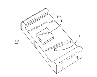
Ref err ing now to Fig _ lA, one em~boaimen t of an enclosure For
a transmitter 10 un_t is illustrated wi:ich may be attached to a
i~:nown fixed iocatic~, presumably at a ca__~.tral location or a
conve::ien~ and accessible area. Th= user may use double sia~a
tGoe, ~' :~CRO~ , or a: y suitab? a method to secu=a the transmits==-,
__ desired. One er::oodiment os an enclosur= for receiver I~ .s
a ~ so =1? us ~r at~d i= Fig . 1B whit.. may b~ at Cached t
ia'Ji~SF_' O~u arv=Cle t:r b°_ lOCat°.~., bV C~CllI~le S=Qed
tape, ZIyL~
C. a:~V Si~=tar?_° mc=hOC. TI: anOthEr (leS1=a'J1~ em~JOdlme~:i. ___-
C=rCtiitrV C~ Lne tranSmlttEr ~s~ 1G and th= reCelVer (S) ~L G=°_
inC'Jrpv~1'ate'.3 ?ii.'_O ...__ eXlStli_~J"- prOdllC~ e-:v_lGSU~=, and 1n ~'e=
SuOi:e?- Ev...~..'7G_m~Ilt, the reC°_iV°_r mcy be c.~~._'-
..D~.~'G LO b°_ lnscr-e.~_,~
-r -r-.= ' -~ _ ri :.~r. ci C form
in ~ ~ e~_=s ~ nc r o,~uct ._~L~ rc ( . c _ , ___ tr= a"
CA 02206520 1997-OS-30 ,
WO 96/18165 PCTI1895101156
_g_
enclosure including the receiver and the. unit batteries where the
housing is structured to replace the existing product's standard
batteries).
Multiple receivers 12 may be used with a single transmitter ,
10. Each transmitter 10 generates and saves a unique
identification code that is recognized by the receivers) 12 so
that the receiver is able to distinguish that particular
transmitter's signal. The -transmitter 10 includes a pushbutton
14, and one indicator, a light-emitting diode 16, as shown.
Referring now to Fig. 2, a block diagram of the transmitter
is shown. The transmitter 10 includes a microprocessor
section 20, which receives clock signals from a clock circuit 22.
A battery circuit 24 supplies power to the microprocessor- section
and also supplies power to an RF section 26. An antenna 28
broadcasts the signal from the output of the RF block 26 which
is activated under control ofthe microprocessor section 20. A
switch 14 attached to the microprocessor section 20 permits
activation of predefined user functions, while an LED 16 provides
user feedback, as will be described below.
Referring now to Fig. 3, an illustrated schematic diagram
of a specif is embodiment of the transmitter 10 is shown . In Fig .
3 the circuitry corresponding to the circuit blocks of Fig . 2 are
enclosed with dashed lines and labelled with the same
corresponding reference numerals. -
In the illustrated embodiment of Fig. 3, the transmitter.l0
includes the microprocessor section 20 essentially comprising an
8-bit EPROM (electrically programmable read-only memory) based
CMOS microprocessor U1 as is well known in the art. The
CA 02206520 1997-OS-30
WO 96/18165 PCTIIB95/01156
-9-
microprocessor Ul in the illustrated embodiment of Fig. 3 is a
PIC16C54LP manufactured by Microchip Technologies.
The clock circuit 22 includes a crystal X1 connected across
a microprocessor inputs OSC1 and OSC2, respectively. A capacitor
C1 is connected between the end of the crystal X1 that is
connected to OSC1, and ground, while a capacitor C2 is connected
from the other end of the crystal to ground. The crystal X1 and
the capacitors C1 and C2 determine the oscillator clock frequency
for the microprocessor U1 as is well known in the art.
The battery test circuit 24 (two blocks are shown connected
together), is shown connected to microprocessor I/O pins RAO,
RAl, and RA2, and includes two batteries B1 and B2, resistors
R1, R2, R3, R4, a zener diode D1, a light-emitting diode LED1,
and a transistor Q1, as shown. The batteries Bl and B2 are
connected in series to supply +3 volts to the circuitry of the
transmitter circuit 10. The connection to the +3V supply point
is labeled +3VDC. The resistor R4 in series with the LED 16 is
connected between the microprocessor Input/output (I/O) pin RA2
and the collector of the transistor Q1, which is further
connected to +3VDC. The LED 16, under microprocessor control is
illuminated when microprocessor I/O pin RA2 is switched to a
logical low. The resistor R1 couples the- collector of transistor
Q1 to its base providing a suitable bias voltage for the
- transistor and is further coupled to the microprocessor I/C pir~
RAO through the series combination of the zener diode D1 and the
resistor R3, as shown. Additionally, the emitter of the
transistor Q1 is coupled to the microprocessor I/O_ pin RA1, which
is further connected to ground through the resistor R2.
CA 02206520 1997-OS-30
WO 9G/18165 PCT/1895/01156
-10-
In operation, in the embodiment illustrated in Fig. 3, the
transmitter 10 will operate whenever the battery voltage is above
2.4 volts, while the microprocessor U1 will function when at
least 2.2 volts is supplied. A battery testing operation is ,
initiated when the microprocessor U1 switches the microprocessor
I/O pin RAO low causing transistor Ql to conduct. This places
the battery voltage +3VDC across resistor R2, which acts a test
load. If the battery voltage drop across resistor R2 is
sufficient to cause a high logic level to be read on the
microprocessor I/O pin RA1, then the battery is considered
functional. Resistor R3 sets the turn-on point for the
transistor Q1, and hence, the hysteresis point for the battery
circuit 24. The LED 16 may be alternately turned-on and off for
a predetermined period of time in response to a failed battery
test by setting the microprocessor I/O pin RA2 low and high,
respectively. The battery test is performed on a demand basis,
that is, it is performed each time the switch 14 is depressed as
will be described below. If the battery test is successful, no
additional user indication is provided and the transmitter enters
a sleep state. If the battery test fails, but there is still
enough battery life to power the transmitter 10, the LED i6
flashes eight times as a user indication and the transmitter
enters a sleep state. Two AAA-type batteries may supply power
to the transmitter 10 for about one year under normal operating ,
conditions.
Power to the microprocessor U1 is supplied through a pin Vdd
while a pin ~lss is connected to ground to complete the circuit.
To permit testing, the microprocessor I/O pin RB4 is pulled-up
CA 02206520 1997-OS-30
WO 96118165 PCT/IB95/01156
-11-
to +3VDC through resistor R5 and is also connected to jumper J1.
When the jumper J1 is installed, grounding microprocessor I/O pin
RB4, the microprocessor U1 is forced into an FCC test mode. In
- this mode, the microprocessor U1 causes a continuous pulse width
modulated signal to be produced so that test measurements may be
taken. The illustrated embodiment of the transmitter 10 meets
the requirements set forth by FCC rules for unlicensed operation
under 47 C.F.R. 15 subpart C.
The RF section 26 of the transmitter_10 includes resistors
R6-R8, capacitors C3-C8, inductors L1-L2, antenna 28, and RF
transistor Q2, as shown. A microprocessor I/0 pin RBO is coupled
to the base of RF transistor Q2 through series resistors R6 and
R7 to provide a signal to turn-on and turn-off oscillation of
transistor Q2, as will be described below.
The RF transistor Q2, arranged in a grounded base
configuration, oscillates at approximately 380.55 Mhz when
microprocessor I/O pin RBO is activated (high). The
microprocessor I/O pin RBO, under software control, provides a
variation of pulse width modulation by varying the duty cycle of
the output signal to essentially provide an amplitude modulated
RF output whose amplitude is either on or off. When the
microprocessor I/O pin RBO is high, transmitter Q2 oscillates.
Conversely, when the microprocessor I/O pin RBQ is low, the
' transistor Q2 is off. Thus, the RF tran-smission is under direct
control of the microprocessor U1. The emitter of the RF
transistor Q2 is coupled to ground through the parallel
combination of the resistor R8 and the capacitor C4. The
combinatior~ of the resistor R8 and the capacitor C4 determines
CA 02206520 1997-OS-30
WO 96/18165 PCT/1895/01156
-12-
the output power level of the RF energy developed at the
collector of the RF transistor Q2.
The collector of the RF transistor Q2 connects to a resonant
tank circuit 36, shown enclosed in dashed lines within the RF
block 26. The tank circuit 36 includes the parallel combination
of inductor Ll, and capacitors C5 and C6, connected to inductor
L2, as shown. The other end of the inductor L2 is connected to
+3VDC. The inductor L2 decouples the low impedanceof the
battery circuit 24 from the tank circuit 36 to allow coupling of
feedback to sustain oscillation of transistor Q2. The capacitor
C7 is connected between the base of the RF transistor Q2 and the
first end of the inductor L2 between the inductor L2 and the tank
circuit 36. The capacitor C7 adds phase shifted energy to the
base of the RF transistor Q2 causing a sustained oscillation.
The capacitor C7 also isolates RF energy within the RF block 26
by providing a shunt path. Thus, little RF energy escapes into
the other sections of the transmitter 10. The quiescent point
of the RF transistor Q2 and, thus, the starting ability of the
oscillatlori is controlled by the reactance of the inductor L2 and
the bias point set by the resistor R7 acting as a voltage- to
current converter.
The oscillation frequency of the transistor- Q2 is
established generally by the capacitor C6 and the inductor L1,
and is fine-tuned by adjusting the value of. the variable ,
capacitor C5. The capacitor C3.connected between ground and the
junction between the resistors R6 and R7 provides signal
smoothing of the square wave signal- supplied' by the
microprocessor I/O pin RBO so that the transistor Q2 turns on
CA 02206520 1997-05-30
wo 96I1~165 PCTIIB95I01156
-13-
"softly". The rise time of the digital pulse train supplied by
the microprocessor I/O pin RBO to the base of the transistor Q2
is shaped by the resistors R6, R7 and the capacitor C3 acting
essentially as-a low-pass filter to smooth the sharp square wave
signal. The antenna 28 (e.g., in the illustrated embodiment, a
nineteen centimeter wire which can be routed within the
transmitter 10 case) is inductively coupled to the tank circuit
36 for external transmission of the RF energy.
The capacitors C8, C9, and C10, connected between the +3VDC
side of the inductor L2 and ground provides RF isolation to
minimize leakage of high frequency signals from the RF block 26
to other sections of the transmitter lo. The capacitors Cs, C9,
C10, C11, and C12 connected between +3VDC and ground also provide
power storage for supplying power to the transmitter 10 for a
limited period of time when the batteries B1 and B2 are removed.
These capacitors allow the microprocessor U1 to temporarily
retain all memory functions when the batteries B1 and B2 are not
installed. Power can be maintained for approximately five
minutes with the batteries Bl and B2 removed.
A microprocessor I/O pin RTCC connected to +3VDC enables an
internal clock counter of the microprocessor Ul. A master clear
input MCLR of the microprocessor U1 is coupled through a resistor
R9 to the common point between a capacitor C13 and a resistor
~ R10. The other end of the resistor R10 connects to +3VDC while
the other end of the capacitor C13 is grounded as shown. The
combination of the resistors R9, R10 and the capacitor C13
supplies a properly shaped reset pulse to the microprocessor U1
at input MCLR when power is initially applied, as is well known
CA 02206520 1997-OS-30
WO 96/18165 PCT/IB95/01156
-14-
in the art. The momentary contact switch 14 connected between
a microprocessor I/O pin RA3 and the common point between the
capacitor C13 and the resistor R10 is provided as a user control,
as will be described below.
When the microprocessor I/O pin RA3 is programmed to be low,
depression of the switch 14 effectively couples the
microprocessor input MCLR to a logic low through the resistor R9,
causing a master reset to occur. When a master reset occurs, if
certain software conditions have been met (described
hereinafter), the microprocessor U1 will activate the
microprocessor .I/O pin RBO to control oscillation of the
transistor Q2. When the microprocessor I/O pin RA3 is programmed
to be high, depression of the switch 14 has no effect. The
switch 14 can be selectively enabled and disabled by the
microprocessor U1.
Table 1 provides examples of typical component values and
part numbers suitable for the embodiment of the transmitter 10
shown in Fig. 3.
TABLE 1 - TRANSMITTER
COMPONENTS
DESIGNATION TYPE VALUE
ANT1 Antenna N/A
gl BATTERY +1.5V
B2 BATTERY +1.5V
C1 CAPACITOR 22pF
C2 CAPACITOR 22pF ,
C3 CAPACITOR 47pF
C4 CAPACITOR 1nF
C5 CAPACITOR 1.7-3pF
CA 02206520 1997-OS-30
WO 96/1165 PCT/1895/01156
-15-
TABL E 1 - TRANSMITTER COMPONENTS
C6 CAPACITOR 6.OpF
C7 CAPACITOR 6.OpF
I
- C8 CAPACITOR 1nF '
C9 CAPACITOR 22uFQ6VDC
C10 CAPACITOR 22uF@6VDC
C11 CAPACITOR 1nF
C12 CAPACITOR 68uF@6VDC
C13 CAPACITOR .OluF
LED1 LIGHT-EMITTING DIODE ANY
D1 ZENER DIODE BZX84C2V7
L1 LOOPCOIL INDUCTOR ETCHED
L2 INDUCTOR 3.9uH
Q1 PNP TRANSISTOR FMMT2907A
Q2 NPN TRANSISTOR FMMT918CT
R1 RES ISTOR l OKS2
R2 RESISTOR 3 9KS2
R3 RES I STOR 3 . 9 KS2
R4 RES I STOR 12 0 S2
R 5 RE S I S TOR 4 7 KS2
R6 RES I STOR 1KS2
R7 RES I STOR 4 7KS2
R8 RESISTOR 6852
R9 RESISTOR 10052
R10 RES I STOR 3 9 KS2
SW1 SWITCH PUSHBUTTON
U1 PIC16C54LP N/A
' X1 CRYSTAL 32.768 Khz
In operation, the transmitter 10 control is user friendly,
since only the switch or pushbutton 14 and the LFD 16 are
available to the user. Once the batteries B1 and B2 are
CA 02206520 1997-OS-30
WO 96/18165 PCT/IB95/01156
-16-
installed, the transmitter 10 automatically creates and transmits
an identification code by pulse width modulating the RF
oscillation of the transistor Q2. This is a variation of pulse
width modulation since the RF energy is either present (i.e.,
during the pulse) or absent (i.e., between pulses). In effect,
this is an amplitude modulation format. The identification code
is automatically created and saved when the user depresses the
pushbutton 14 after installation of the batteries B1 and B2.
Alternatively, if the pushbutton 14 is not depressed within eight
minutes after the batteries B1 and B2 are installed, a default
value is selected as the identification code. In either case,
the identification code selected corresponds to the value of a
unique eight bit number. Initial installation of the batteries
B1 and B2 may not trigger creation of the identification code.
Rather, after battery installation, the user may depress the
pushbutton 14 to begin the process and depresses it again to
terminate the process.
In one embodiment, the- identification code may be
transmitted once- the pushbutton 14 is depressed. The
identification code is transmitted as fellows: First, a
preamble code is transmitted consisting of 30 milliseconds on
(logic high) followed by 10 milliseconds off (logic low). This
is repeated five times for a total preamble of about 200
milliseconds. Note that when the microprocessor U1 turns-on ,
transistor Q2, the 380.55 Mhz RF energy is broadcast. During the
time when the preamble is being transmitted, the receiver 12 is
activated in the designated frequency region to search for the
CA 02206520 1997-OS-30
WO 96/18165 PCT/IB95/01156
-17-
known preamble code. After the code has been transmitted five
times, the identification code is transmitted.
Transmission of the eight bit code (not including the
- preamble) occurs as follows: A logical one or high is indicated
by 20 milliseconds on followed by 10 milliseconds off, while a
logical zero or low is indicated by 10 milliseconds on followed
by 10 milliseconds off. This cycle is repeated for each of the
eight bits of. the identification code until the entire
identification code has been is transmitted. The entire sequence
of the preamble code and code transmission is continuously
repeated for a period of time of about between 5.4 seconds to 6.6
seconds in the illustrated embodiment. During this time, the
receiver 12 first recognizes the preamble code,- and then
receives, decodes, and saves the identification code. The result
is synchronization of the receiver 12 to the unique transmitter
identification-code.
Referring now to Fig. 4, a block diagram of one embodiment
of the receiver 12 is shown having eight major blocks 40-54, as
shown. The receiver 12 includes a microprocessor block 40, which
receives clock signals from a clock block 42. A battery circuit
44 monitors battery power and supplies power to the
microprocessor section 40 and to other blocks of the receiver 12.
An amplifier block 46 receives RF energy from an antenna 47 and
passes an amplified signal to a super-regenerative -detector block
48. The super-regenerative detector block 48, determines the
presence of RF energy at a preselected frequency and passes its
output to a differentiator block 50. The signal processed by the
differentiator block 50 is coupled to a shaping c-ircuit block 52,
CA 02206520 1997-OS-30
WO 9G/18165 PCT/IB95/01156
-18-
whose output is coupled to the microprocessor block 40. The
microprocessor section 40 controls an alarm block 54 which drives
an audio indicator block 56, under software control.
The battery circuit block 44 supplies power to the ,
microprocessor block 40, the super-regenerative detector block
48, the differentiator block 50, the alarm block 54, and the
shaper block 52. However, the microprocessor block 40 directly
controls power to the amplifier. block 46, as shown by a line
labeled +vs so that power can be selectively turned-off under
microprocessor control to conserve power when not needed, for
example, when the microprocessor block 40 enters a "sleep" mode
as will be described hereinafter.
Referring now to Fig. 5, an illustrated schematic diagram
of one embodiment of the receiver 12 of Fig. 4 is shown. In Fig.
, the circuity corresponding to the circuit blocks of Fig . 4 are
enclosed within dashed lines and labelled with the same
correspondence reference numerals.
The amplifier block 46 as shown, includes a transistor Q3,
resistors R20-R23, capacitors C20-C24, coupled to the antenna 47.
The receiver 12 is a super-regenerative detector and, thus,
typically emits a certain amount of radio frequency noise which
must be minimized to comply with FCC regulations. Theprimary
purpose of the amplifier block 46 is to isolate, as much as
possible, any RF energy created by the super-regenerative
detector block 48 such that the RF energy is not radiated through
the antenna 47.
Radio frequency signals 60 received by the antenna 47 are
capacitively coupled to the amplifier block 45 through a
CA 02206520 1997-OS-30
WO 96118165 PCT/IB95/01156
-19-
capacitor C20 into the emitter of a transistor Q3. The emitter
of the transistor Q3 is further coupled to ground through the
parallel combination of a resistor R23 and a capacitor C24 , which
- partially governs the gain and isolation of the amplifier block
46. Resistors R20 and R22 form a voltage divider network to bias
transistor Q3 to a desired operating point . Capacitor C21 places
the base of Q3 at RF ground, thus grounded base operation of this
stage is obtained for maximum isolation. The collector of the
transistor Q3 is coupled to voltage +Vs through a resistor R21,
while a capacitor C22 connected between voltage-+Vs and ground
provides energy storage and filtering for noise on the supply
line.
The output of the amplifier block 46 developed at the
collector of the transistor Q3 -is coupled to the super-
regenerative detector block 48 through a coupling capacitor C23,
as shown. The amplifier block 46 functions as a broad-band
amplifier and does not include any tuning or filtering circuitry.
Although the amplifier block 46 provides gain, its primary
purpose is to isolate RE energy to prevent it from being coupled
backwards from super-regenerative detector circuit 48 and to the
antenna 47. A wide variety of suitable isolating amplifiers may
be used for the amplifier block 46 of the illustrated embodiment .
The output of the amplifier block 46 is routed into the
super-regenerative detector block 48 through the capacitor C23
and includes a transistor Q4, resistors R24-R28, capacitors C25-
C28, inductors L5-L6, and a diode D5. The transistor Q4 is
configured to oscillate near 380.55 Mhz by the resonant action
of the inductor L5 and the capacitor C26. The capacitor C25
CA 02206520 1997-OS-30
WO 96/18165 PCT/1895/01156
-20-
couples the energy from the collector into the base of the
transistor Q4 to maintain oscillation and provide a degree of
frequency selectivity for the received signal. The resistor R28
provides isolation of the collector RF signal from the lower
impedance battery power circuit 44.
Temperature stable operating bias is established for the
transistor Q4 by the voltage divider action of the resistors R26
and R27, and the diode D5 provides temperature stabilization.
Oscillations build up and extinguish (quench) in this stage at
an approximate rate of 100,000 cycles per second. This desirable
quench mechanism is controlled by the selection of the capacitors
C27, C28, and the inductor L6_ The resistor R24 provides
additional operating point bias stabilization.
When a signal is received within the super-regenerative
detector's tuned circuit passband, the quenching action is
increased substantially and higher current quench oscillations
are sustained providing 100 Khz current pulses across the
resistor R24 coincident with the carrier presence of the received
pulse width modulated signal. Many pulses of 100 Khz energy from
the quenching action are received for each burst of 380 Mhz
signal providing the extreme detection gain typical of super-
regenerative detectors. The resistor R14 provides isolation to
the RF and quench signals present at the resistor R24 and the
inductor L6 junction, and it also provides desired coupling with -
very little attenuation to the 100 Khz signal passed on to the
capacitor C24.
The 100 Khz signal is -filtered and processed,by the
differentiator block 50. This block 50 receives a 380.55 Mhz
CA 02206520 1997-OS-30
WO 96118165 PCT/1895/01156
-21-
pulse width modulated signal and outputs 100 Khz pulses while the
380.55 Mhz signal is present. This is the same frequency at
which the transmitter 10 operates. The tank circuit 62 is fine
tuned by the capacitor C26 to be centered at approximately 380.55
Mhz with a tolerance of about ~50 Khz. Thus, the super-
regenerative detector 48 is responsive to signals between 380.500
Mhz and 380.600 Mhz. The super-regenerative detector 4_8 requires
very little power. Although a super-heterodyne type-receiver may
alternatively be used to provide increased selectivity over the
illustrated super-regenerative detector- 48, it would draw
substantially more current. The super-regenerative detector 48,
although not as selective as a super-heterodyne detector, is
extremely sensitive and requires very little power. For example,
the sensitivity of the receiver 12, including the super-
regenerative detector 48 , is such that it can detect an input
signal received on the capacitor C20 of the amplifier block 46
of between -100 dBm to -105 dBm, (which is equivalent to about
2 microvolts) in a 1 Mhz bandwidth.
As described above, the value of the inductor L5 and the
capacitor C26 of the tank circuit 62 are selected so that the
super-regenerative detector 48 is sensitive only to RF energy at
approximately 380.55 Mhz ~ 50 Khz, which corresponds to the
frequency of the transmitter_ 10. Accordingly, amplitude
~ modulated RF energy between 380 Mhz and 381 Mhz received at the
input 62 of the tank circuit 48 will be detected while RF energy
outside of the frequency range will have no effect on the desired
operation. '
CA 02206520 1997-OS-30
WO 96/18165 PCT11895/01156
-22-
The output of~ the transistor Q4 .is developed across the
resistor R24 which provides the output signal voltage level for
coupling into the next stage. The resistor R25 connected to the
common junction between the inductor L6 and the resistor R24 ,
forms an isolation resistance for supplying the output of the
super-regenerative detector 48 to the -input of the pulse
differentiator block 50 without loading the signals present
across R24. When a transmitter signal is received, the super-
regenerative detector 48 output is a stable source of 100KHz
pulses, thus, the input to the pulse differentiator block 50 is
present and follows the pulse width modulation of the carrier
signal.
Alternatively, a super-regenerative type receiver 12 need
not be used. For example, the front end of the receiver 12 which
includes the antenna 47, the amplifier black 46, and the super-
regenerative detector block 48, may be replaced -with a super-
heterodyne receiver. In addition, in alternative systems using
an infra-red, optical, or other communication medium, an infra-
red receiver, a fiber optic receiver, or any other suitable
receiver -capable of receiving corresponding coded transmitter
signals may be used.
The pulse differentiator block 50 includes an operational
amplifier U3, resistors R29-R31, and capacitors C29-C31.
Operational amplifier U3 is configured as a self-centering high- ,
gain comparator acting as a differentiator. The input to the
differentiator block 50, provided by the output of the super-
regenerative detector block 48 through the resistor R25,~ connects
to the commo:~ junction between the resistors R29 and R30. The
CA 02206520 1997-OS-30
WO 96/1165 PCTIIB95/01156
-23-
resistors R29 and R30 connect to an inverting input 70 and a non-
inverting input 72 of the operational ampli fier U3 , respectively.
The capacitor C29 is connected from the junction of the resistors
- R29 and R30 to ground while the capacitor C30 provides an
integrated level of ZOOKHz pulses to the non-inverting input 72
of the operational amplif.ierU3. The resistor R31 provides
feedback for the operational amplifier U3 by coupling an output
74 of the operational amplifier to the non-inverting input 72.
The capacitor C31 is coupled between +3VDC and ground.
Typically, the resistors R29 and R30. are chosen to be of
equal value. Only the difference between signals present on the
inverting 70 and non-inverting input 72 of the operational
amplifier U3 are amplified. The capacitor C30 provides an
averaging function so that the 100KHz pulse signals present at
the non-inverting input 72 of the operational amplifier U3
charges the capacitor C30 to an average value. Thus, signals
entering the differentiator block 50 through the resistor R25
charge the capacitor C30, which tends to .hold the long term
charge at the non-inverting input 72 of the operational amplifier
U3 . Consequently, such sho.Y. t term changes on the inverting input
70 cause the operational amplifier U3 to differentiate the
signal. Since the capacitor C30 holds an average charge over
time, any change in input signal causes a corresponding change
- in voltage across the input of the operational amplifier U3.
Thus, a change in signal voltage over time is detected at the
inputs to the operational amplifier U3, and that difference is
amplified and an output signal 74 is generated. The gain of the
operational amplifier U3 is governed by the value of the feedback
CA 02206520 1997-OS-30
WO 96/18165 PCT/IB95101156
-24-
resistor R31 divided by the value of R29. (e.g. a gain of 68 in
the illustrated embodiment).
The output of the pulse differentiator block 50 is coupled
to the pulse shaper block 52 through a coupling capacitor C32, ,
connected as shown, from the output of the amplifier U3 to an
inverting input 80 of an operational amplifier U4. The pulse
shaper block 52 includes the operational amplifier U4, resistors
R32-R36, and capacitors C32 and C33. This pulse shaper 52 is
essentially a comparator circuit which produces a sharp square
wave output suitable for input into a digital device. A
connection to +3VDC and ground supplies power to the operational
amplifier U4, as is well known in the art.
The inverting input 8D of the operational amplifier U4 is
also coupled to the resistor R32, while the non-inverting input
82 of the operational amplifier U4 is coupled to the resistor
R33. The other ends of the resistors R32 and R33 are connected
together and are further coupled to a reference voltage derived
from the +3VDC through the resistor R34, as shown. The common
junction between the resistors R32, R33, and R34 are additionally
coupled to ground through the parallel combination of the
resistor R35 and the capacitor C33 to provide a stable voltage
reference for U4. The resistor R36 connected between the non-
inverting input 82 and an output 84 of the operational amplifier
U4 provides the required hysteresis.
The input signal to the pulse shaper block 52 received at
the inverting input 80 of the operational amplifier U4 is .
approx'itriately 600 millivolts and swings about 1D0 millivolts when
the output of the pulse differentiato~-circuit 50 changes state
CA 02206520 1997-OS-30
WO 96/1$165 PCT/IB95/01156
-25-
in response to a received RF signal 60. When the signal present
at the inverting input 80 of the operational amplifier U4 exceeds
the reference voltage present at the non-inverting input 82, the
operational amplifier saturates and provides an output at a
digital logic low level. Otherwise a digital high logic level
is generated on the output 84 of the operational amplifier U4.
This digital output signal is coupled, as shown, to the
microprocessor 40. _._
In the illustrated embodiment of Fig. 5, the microprocessor
40 comprises an 8-bit EPROM based CMOS microprocessor U5, as is
well known in the art. The microprocessor U5 is a model
PIC16C54LP manufactured by Microchip Technologies, as disclosed
publication DS30015H from Microchip Technologies, and is
identical to microprocessor U1 shown in Figures 2 and 3.
A clock circuit 42 includes a crystal X2 connected across
microprocessor inputs OSC1 and OSC2. A capacitor C34 is
connected from the terminal of the crystal X2 that is connected
to microprocessor pin OSC1 to ground, while a capacitor C35 is
connected from the other end of the crystal to ground. The
crystal X2, and the capacitors C34 and C35 determine the
oscillator clock reference for the microprocessor U5, as is well
known in the art.
An alarm block 54 includes transistors Q5 and Q6, resistors
R37-R38, a capacitor C36, a diode D6, and an audio indicator 56,
as shown. A microprocessor Z/O pin RB7 is coupled to_ the base
of the transistor Q6 through the resistor R38 controls operation
of the audio alarm circuit 54. The microprocessor T/O pin RBA
turns the alarm indicator 56 on and off by prozriding a logic high
CA 02206520 1997-OS-30
WO 96/18165 PCT/1895/01156
-2~=
and logic low, respectively, to the base of the transistor Q6.
The collector of the transistor Q6 is coupled to the base of the
transistor Q5, while the emitter of the transistor Q6 is
grounded. The collector of the transistor Q5 is coupled to the
base of the transistor Q6 through the series combination of the
resistor R37 and the capacitor C36.
The collector of the transistor Q5 is connected to one end
of the audio indicator 56, which may be a moving coil type audio
device, such as a miniature speaker , as is well known in the art .
However, any suitable audio or visual indicator which alerts the
user may be used. The collector of the transistor Q5 is
additionally connected to the cathode of-the diode D6 while the
anode of the diode D6 is connected to the other end of the audio
indicator 56 and ground. Transistor Q5 and Q6 form a-transistor
oscillator circuit that is turned on and off by appropriate logic
levels supplied by the microprocessor I/O pin RB7. The
transistors Q5 and Q6 provide the drive current necessary to
activate the audio indicator 56 while the capacitor C36 and the
resistor R37 determine the frequency of oscillation, and hence,
the tone of the audio output.
A battery circuit 44 (two blocks are shown connected
together to form the battery circuit), includes two conventional
batteries B3 and B4 connected in series-to supply +3VDC to the
receiver 12 in the illustrated-embodiment. This circuit is
similar to tle battery circuit 24 shown in Figs. 2 and 3. The
common connection to the +3 volt supply point is labeled +3VDC.
Power is supplied to the microprocessor TJ5 through a power pin
Vdd while a ground pin Vss completes the circuit. The_=battery
CA 02206520 1997-OS-30
WO 96/18165 PCT/1B95101156
-27-
circuit 44 couples to microprocessor I/O pins RAO and RA1, and
includes resistors R39-R41, a zener diode D7, and a transistor
Q7. The resistor R41 couples the collector of transistor Q7 to
its base thereby providing a bias voltage. The junction between
the collector of the transistor Q7 and the--resistor R41 is
connected to +3VDC. The base of the transistor Q7 is coupled to
the microprocessor I/O pin RAO through the series combination of
the resistor R39 and the zenerdiode D7. Additionally, the
emitter of the transistor Q7 is connected to the microprocessor
I/O pin RA1 which is further coupled-to ground through the
resistor R40.
The capacitors C37, C38, and C39 are connected between +3VDC
and ground to provide power storage for supplying power to the
receiver circuit 12 for a limited period of time when the
batteries B3 and B4 are removed. During that period of time, the
microprocessor U5 will retain all program and memory functions
for a period of about five minutes.
In operation, the battery testing operation is initiated
periodically under microprocessor control when the microprocessor
U5 lowers the I/O pin RAO causing the transistor Q7 to conduct.
This places the battery voltage +3VDC across the resistor R40,
which acts as a test load. If the voltage drop across the
resistor R40 is sufficient to cause a high logic level to be read
' on the microprocessor I/O pin RAl, the battery is considered to
be functional. The resistor R39 sets the hysteresis point for
the battery circuit.
A microprocessor I/O pin RTCC connected to +3VDC enables an
internal clock counter of the microprocessor 40 (U5). A master
CA 02206520 1997-OS-30
WO 96!18165 PCT/IB95/01156
-28-
clear input MCLR of the microprocessor 40 (U5) connects to a
common connection between a capacitor C40 and a resistor R42.
The other end of the resistor R42 connects to +3VDC while the
other end of capacitor C40 is grounded. This supplies a properly
shaped reset pulse to the microprocessor U5 upon application of
power, as is well known in the art. In addition, the
microprocessor 40 (U5) supplies a selectively enabled voltage +Vs
through a limiting resistor R43 from an output port RA2 to the
amplifier block 46. As previously described, this allows power
to the amplifier 46 to be selectively turned-off under
microprocessor control to conserve power.
A first terminal of- a motion sensitive switch 86 is
connected to a microprocessor I/O pin RB4 while the other end of
the switch is pulled-up to +3VDC through a resistor R44. The
junction between the resistor R44 and one terminal of the motion
sensitive switch 86 is coupled to a microprocessor I/O pin RB5.
The switch 86 may be a mercury switch or any other suitable
motion sensitive device as are well known in the art.
In operation, when the receiver 12 is stationary, the switch
86 is 1n one particular state that is read and stored by the
microprocessor 40 (U5). When the transmitter 10broadcasts its
identification code and the receiver 12 responds by activating
the audio alarm 56, the user may locate the receiver and
terminate the audio alarm by moving or shaking the receiver. _
This shaking or moving the receiver causes the motion sensitive
switch 85 to change states. Such a change in state is sensed by
the microprocessor 40 (U5) which then terminates the audio alarm
under program control. Physically shaking the receiver 12 may
CA 02206520 1997-OS-30
WO 96/18165 PCT/IB95/01156
-29-
cause the motion sensitive switch 86 to change states many times .
Such switch "bounce" is properly interpreted by the
microprocessor 40 (U5) as motion of the receiver.-
Table 2 provides examples of typical component values and
part numbers, where applicable, for the embodiment of the
receiver shown in Fig. 5.
TABLE 2 - RECEIVER
COMPONENTS
DESTGNATION TYPE VALUE
AUDI AUDIO INDICATOR 1652
ANTI ANTENNA WIRE
g3 _ BATTERY +1.5V
B4 CAPACITOR +1.5V
C20 CAPACITOR 330pf
C21 CAPACITOR 330pF
C22 CAPACITOR 1nF
C23 CAPACITOR 0.5pF
C24 CAPACITOR 6.Opf
C25 CAPACITOR 33pF
C26 CAPACITOR 3-lOpF
C27 CAPACITOR 390pf
C2g CAPACITOR 4pF
C29 CAPACITOR 1nF
C30 CAPACITOR luFC~5VDC
C31 CAPACITOR 1nF
C32 CAPACITOR 1nF
C33 CAPACITOR lOnF
C34 CAPACITOR 22pF
C35 CAPACITOR 22pF
C36 CAPACITOR 3.3nF
C3~ CAPACITOR 68uFC~6VDC
C38 CAPACITOR 1nF
CA 02206520 1997-OS-30
WO 96/18165 PCT/IB95/01156
-30-
TABLE 2 - RECEIVER
COMPONENTS
DESIGNATION TYPE VALUE
C39 CAPACITOR 22uF@6VDC
C40 CAPACITOR lOnF
D5 DIODE MMBD914XT1
D6 DIODE MMBD914XT1
D7 ZENER DIODE BZX84C2V7PH
L5 INDUCTOR 21.6nH
L6 INDUCTOR lOuH
Q3 NPN TRANSISTOR FMMT918CT
Q4 NPN TRANSISTOR FMMT918CT
Q5 PNP TRANSISTOR FMMT2907A
Q6 NPN TRANSISTOR MMST2222
Q7 PNP TRANSISTOR FMMT2907A
R20 RESISTOR 51KS2
R21 RESISTOR 1KS2
R2 2 RES I STOR 2 2 KS2
R23 RESISTOR 27052
R2 4 RES I STOR 6 . 8 KS2
R2 5 RES I STOR l O KS2
R2 6 RES I STOR 3 9 KS~2
R2 7 RES I STOR 7 5 KS2
R2 8 RESISTOR 3 . 9KS2
R2 9 RE S I S TOR 10 0 KS2
R3 0 RES I STOR l 0 0 KS2
R31 RES I STOR 6 . 8MS2
R3 2 RES I STOR 4 7 0 KS2
R33 - RESISTOR lOKS2
R3 4 RES I STOR 4 7 KS2
R3 5 - RES I STOR 4 7 KS2
R3 6 RES I STOR 6 . 8MS2
R37 RESISTOR _ lOKS2
CA 02206520 1997-OS-30~
WO 96/18165 PCT/IB95/01156
-31-
TABLE 2 - RECEIVER
COMPONENTS
DESIGNATION TYPE VALUE
R38 RESISTOR 220KS2
R3 9 RES I STOR 3 . 9 KS2
R4 0 RES I STOR 3 9KS2
R41- RE S I S TOR 10 KS2
R42 RES I STOR 3 9 KS2
R4 3 RES ISTOR 3 . 9KS2
R4 4 RES ISTOR 4 7KS2
SW2 MOTION SWITCH DURAKOOL-4859
U3 OPERATIONAL MAX407CSA
AMPLIFIER
U4 OPERATIONAL MAS407CSA
AMPLIFIER
U5 MICROPROCESSOR PIC16C54LP
X2 CRYSTAL 32.768 Khz
Referring now to Fig. 6, there is shown- a flowchart
illustrating a specific embodiment of the logical flow of a
transmitter program 99 wherein the unique identification code is
created and transmitted. The transmitter program 99 provides for
a simple and low cost generation of unique identification codes.
Creation of the unique identification code is referred to as
transmitter serialization. Once generated, the transmitter
identification codes are electronically accessible to other
programmed devices, such as the receiver 12-. The process of
creating the identification code utilizes the fact that
microprocessors and other computing devices generally require a
synchronizing clock signal input. Given a sufficiently high
clock rate, human controlled time intervals measured relative to
that clock can be used to create essentially unique values.
CA 02206520 1997-OS-30
WO 96/18165 PCT/IB95/01156
-32-
The serialization process creates a pseudo-random
identification code that is derived from a counter which is
continuously incremented under software control. A user action,
such as pressing the pushbutton 14, halts incrementing of the y
counter-to yield a unique identification number.
. However, the transmitter program 99 is not a truly linear
procedure as it might appear from the flowchart of Fig. 6. The
transmitter program 99 may be entered due to several different
occurrences, all causing a microprocessor reset. In the
illustrated embodiment, such occurrences include: 1) initial
application of power causing a power-up reset, 2) depression of
the pushbutton 14 on the transmitter 10, and 3) a watchdog
timeout.
The transmitter program 99 begins as shown in step 100.
Next, various sections of hardware are initialized, such as
registers, memory locations, I/O ports, and the like, as
illustrated in step 102. As indicated by step 104, the software
determines whether entry into this routine was caused by a
watchdog timeout. Step 104 is an error condition and should
rarely occur . If , however, such an event does occur, the program
branches to step 106. If entry into the transmitter program 99
was not caused by a watchdog timeout, a determination is made as
to whether entry was caused by depression of the -pushbutton 14
while in the sleep state, as shown in step 108. ,
One feature of the microprocessor 20 (U1) is the ability to
enter a "sleep state" where power consumption is significantly
reduced, yet memory functions are retained. The microprocessor
20 "awakes" or exits the sleep state when a master clear input
CA 02206520 1997-OS-30
WO 96/18165 PCT/1895/01156
-33-
(Fig. 3, microprocessor pin MCLR) is brought low. In one
embodiment, the master clear input MCLR may be activated from a
variety of sources as described above. Note that the pushbutton
14 may be depressed when the user wishes to locate the receiver
12 or may be depressed to program or synchronize the receiver.
Ifentry into the routine was not caused by depression of
the pushbutton 14 while in the sleep state, as shown in step 108,
then it is assumed that entry has been caused by a power-up reset
condition caused by initial application of battery power or
depression of the pushbutton 14 while synchronizing, as
illustrated by the "no" branch of step 108. Next, in step, 110,
a variable labeled variable) (VAR1) is checked to see if it
contains the value of 41, while a variable labeled variable2
(VAR2) is checked to see if it contains the value of 42. If
variable) and variable2 are not equal to the predetermined
values, then the variables are checked to determine whether
variable) and variable2 are equal to a counter value, as shown
in step 112. It should be noted that any suitable predetermined
value may be used, and the software is not limited to the use of
the values of 41 and 42 respectively.
The counter value is the value of an internal counter used
to store the unique identification code. The value of the
counter is written into variable) and variable2, shown in step
114, as will be described below. Variable), variable2, and the
counter value (VAR2a) being equal indicates that the
identification code had already been determined and saved, and
that a momentary loss of power occurred, but not sufficient to
cause a loss of memory. If the three values are equal, as shown
CA 02206520 1997-OS-30
WO 96/18165 PCT/iB95/01156
-34-
by the "yes" arrow in step 112, the software branches to step
116.
If variablel, variable2 and the counter-value are not all
equal, then variablel is set equal to 41, variable2 is set equal ,
to 42, and the pushbutton 14 is enabled, as shown in step 118.
Step 118 is the beginning of a serialization portion 119 of the
transmitter program 99. Enabling the pushbutton 14 under
software control allows subsequent depressions of the pushbutton
to be sensed by the microprocessor. Next, as shown in step 120
the counter value is continuously incremented over a period of
time of up to eight minutes, as illustrated in step 122. If
eight minutes has not elapsed, as shown in the "no" branch of
step 122, the software branches back to step 120 and continues
to increment the counter. During the eight minute period of
time, the user may depress the pushbutton 14 so as to create the
unique identification code from the counter value, as will be
described below.
The time between insertion of the batteries to when the user
depresses the pushbutton 14 represents a unique period of time
and thus, a unique counter value is generated that can be used
as an identification code. Therefore, when the user depresses
the pushbutton 14 within the eight minute period of time, the
serialization routine is interrupted and reentered, since °
depression of the pushbutton causes a master reset occurrence. .
However, during this reentry, all memory values previously saved
remain intact and. indicate what actions have already been
performed. Thus, when step 110 is again reached, variablel does
equal 41 and variable2 does equal 42, indicating that code
CA 02206520 1997-OS-30
WO 96/1165 PCT/IB95/01156
-35-
creation was in progress at the time the pushbutton 14 was
depressed. Accordingly, as shown in the "yes" branch of step
110, the routine branches to step 114 where the counter value is
stored into variable) and variable2, respectively, as the unique
identification code. If the user does not depress the pushbutton
14 within the eight minute period of time, as indicated in step
122, at the end of eight minutes the pushbutton 14 is disabled
as shown in step 124 , and the current value of the counter is
assigned as the default identification code.
After either the default identification code has been
assigned, or a counter value has been stored in response to a
pushbutton 14 depression, the program continues at step 116. To
summarize, step 116 may be reached through several different
occurrences. First, the pushbutton 14 may have been depressed
while transmitter is in the sleep state, as shown by the "yes"
branch of step 108. Second, if variable) and variable2 and the
count value are all equal, as shown in the !'yes-" branch of step
112, a brief power failure causing a master reset without loss
of memory is indicated. Third, a branch from step 114 after
creation of the initial identification code causes the software
to branch to step 116.
The serialization portion 119 of-the transmitter program 99
begins at step 118, ends at step 114, and includes intermediate
steps 120, 122, and 124. To perform the serialization steps, two
consecutive entries into the transmitter program 99 must have
occurred. The first entry occurs whenthe batteries are
initia411y installed with power comnletely drained 'from the
transmitter. During this first entry, steps, 100, 102, 104, 108,
CA 02206520 1997-OS-30
WO 96/18165 PCT/IB95/01156
-36-
110, 112, 118, 120, and 122 are performed with steps 120 and 122
being continuously repeated until either eight minutes has lapsed
(step 122) or the pushbutton 14 is depressed.
Depressing the pushbutton 14 while executing steps 120 and
122 of the serialization portion 119 causes another reset and
subsequent reentry into the receiver program 99. During this
second entry, steps 100, 102, 104, 108, 110, and 114 are
executed. The program does not follow the "yes" branch of step
108 since that branch is only followed while the transmitter is
in the sleep state- during depression of the pushbutton 14.
During steps 120 and 122 the transmitter is obviously not in the
sleep state. Thus, the second depression of the pushbutton 14
causes the serialization portion 119 to fully execute and
generate the unique identification code, as shown in step 114.
Once the software reaches step 116, the LED 16 is turned-on
and a repeat counter is initialized to the value 15. Next, as
shown in step 126, the identification code (the counter value).
is transmitted 15 times. Next, if an FCC test bit is set low,
as shown in step 128, the software continuously branches back to
step 116to repeat transmission of the identification code. If
the FCC test bit is not set low, the LED 16_is turned-off and a
battery test is performed, as indicated in step 130. If the
battery test is successful, as shown in the "no" branch of step
132, the LED 16 is turned-off, the pushbutton 14 is enabled, and .
the transmitter 10 is turned-off to conserve power, as shown in
step 106.
Next, the transmitter 1Q .is placed into sleep mode, as
illustrated in step 134, to await the futuredepressions of the
, CA 02206520 1997-OS-30
«'O 96II8I6~ PCT/IB9~/OI1~6
..
pushbutton o~ other actions w~.ich may cause a master clear reset.
If. the baste-y test fails, as shown in the "yes" branch of step
132, the LED 16 is flashed eight times, as shown in step 136, and
the program branches to step 106.
It shou? d be noted that this process generates pseudo-random
inent~_ficat=on codes that are neither consecutive nor related.
4:hile not an absolutely uniaue number, such a number is
eyfectively unique since the time between when the user installs
. the batteries and presses the pushbutton 14 is highly likely to .
be different each time the user performs the cperatien. In the
u=?='_kelv event that the identi-ication code is net uniaue, the
~PY~Glizaticn process can be repeated to yield the required
un iaue ident_ficatior~ code _
fH Once t'_~_e unique transmitter identification code has been
created ar~d transmuted, the receiver mus~ be programmed to
s
respond only to that transmitter's identification code. The
process of coordi natincr the receiver to the unique identification
code is ca__ed receiver ~synchronization_,
- Referring now Figs. 7; 7A, 7Fs and 7CVthere are flowcharts showing a
spec===c~e~bcd-ment c= the logica? flow ef the receiver progra.«
:~99 . I:owe v e- , the -°ceiver program 199 is not truly a linen=
pros=a;; as -=ght app°ar to be indicated by th° flow chart since
Y r be e_-_=eyed due to S=Veral C.=.==°-rent OCCUrrenCeS,
t he v- ~g~ aW, t:.ay - _ -
al 1 ca~~sinc a microtY.~cessor reset. First, a true power-Lp reset
th=:u'..~, . aW -_-Ca~iG n ._.- ln;tlal E! °ctrlCclG._~.V;=1" IUcy'
CcLISE e_':~.=~,.
CA 02206520 1997-OS-30
WO 96/18165 PCT/iB95101156
-38-
into the routine. Second, a watchdog timer may expire while the
program is executing (not in sleep state) causing a reset- and
subsequent re-entry into the routine. Third, the microprocessor
4 0 (U5 ) may be brought out of a - sleep state by a master clear _
occurrence, and fourth, the routine may be entered due to a
periodic.reset caused by a watchdog timer while the receiver is
in the sleep state (not executing).
The illustrated embodiment of the receiver program 199
begins as shown in step 200. A variable "motion" is set to false
indicating that no motion is sensed from the motion sensitive
switch 86, as illustrated in step 202. Next, various sections
of the hardware are initialized such as- registers, memory
locations, I/O ports, and the like, as indicated in step 204.
As shown in steps 206, 208, 210 and 212, the type of the
reset which caused entry into the routine is determined. In step
206, if a reset was caused by a true power-up condition, such as
when the batteries are inserted, process control branches to step
214. Step 214 represents the initial step of a receiver
synchronization portion 215 of the receiver program 199. If the
watchdog timer has timed-out while the program is executing, as
shown in step 208, causing a reset, the receiver program 199
branches to step 216. If a reset occurs due to the
microprocessor 40 (U5) being brought out of a sleep condition due
to a master clear, the program branches- to step 218, as .
illustrated by the "yes" branch of step 210. This is an error
condition and should rarely occur. If neither step 206, step
208, nor step 210 indicate the cause of the reset leading to
entry of the routine, then entry into the routine must have been
CA 02206520 1997-OS-30
WO 96/18165 PCT/1895/01156
-39-
caused by the periodic reset caused by the watchdog timer, which
occurs approximately every two seconds, as shown in step 212.
The watchdog timer causes the microprocessor 4-0 (U5) to awake
from a sleep state every two seconds to perform receiver
processing, and thus, conserve power.
Referring back to step 206, if the reset was caused by a
power-up reset, a variable labeled variable3 (VAR3) and a
variable labeled variable4 (VAR4) are set to a value of zero and
the program branches to step 220 where the watchdog timer is
reset. Next, the microprocessor 40 (U5) is put into a sleep
state to await a subsequent reset, as illustrated in step 222,
indicating the end of the routine. A value of zero written into
variable3 and variable4 indicates during a subsequent inspection
of the variables that the receiver 12 has not yet been
synchronized to the transmitter code and thus, will not respond
to the transmitter-10. When variable3 and variable4 are later
inspected during subsequent entry into the routine, a zero value
directs the software to save the incoming code as the initial
identification code and thus, the receiver will only respond to
that code during subsequent receiver operations, as will be
discussed hereinafter. The variable3 stores the identification
code such that the receiver may respond to a first transmitter
while variable4 stores a second identification code such that the
receiver may respond to a second transmitter.
If the reset and subsequent entry into the routine was
caused by a watchdog timeout while the program is executing, as
shown in step 208, the audio indicator parameters are set to
produce two sets of four short beeps, as shown in step 216.
CA 02206520 1997-OS-30
WO 96/18165 PCT/IB95101156
-40-
Next, the program branches to step 230 where the alarm subroutine
is called to output the beeps according to the previously
specified parameters. Occurrence of a watchdog timer time-out
while the program is executing represents an error condition and
should rarely, if ever, occur.
If the reset and subsequent entry into the routine was
caused by a master clear while in the sleep state, as shown in
step 210, the program branches to step 218 where the alarm
routine parameters are set to produce two sets of three short
beeps. The software then branches to the alarm subroutine to
output the beeps according to the previously specified
parameters, as shown in step 230. This is an error condition and
indicates a temporary power failure sufficient--to trigger a
power-up reset, but not sufficient to cause memory loss.
After step 230, a battery test is performed, as shown in
step 232 where the battery timer is set up as to force a battery
test. Then the battery test timer is decremented in step 234,
followed by a check to determine whether it. is time to perform
the battery test, as indicated in step 236. If- it is not yet
time to perform the battery test, as illustrated by the "no"
branch of step 236, the process control branches to step 220
where the watchdog timer is reset. If it is time to perform the
battery test, as shown in the "yes" branch of step 236, the
battery test is performed, as indicated in step 238, and the test ,
result is inspected, as shown in step 240. If the battery test
is successful, the process control branches to step 220 where the
watchdog timer is reset. However, if the battery test~fails, as
shown in the "yes" branch of step 240-, the motion sensitive
CA 02206520 1997-OS-30
WO 96/18165 PC7fYyB95/01156
-41-
switch 86 is disabled, as illustrated in step 242, and the alarm
subroutine parameters are set to produce one set of eight short
beeps, as indicated in step 244. The alarm subroutine is then
called, as shown in step 246, to output the audio tones, and the
process control branches to step 220 where the watch dog timer
is reset.
Referring back to step 212, the routine has reached this
step when the periodic watchdog timer, occurring every two
seconds, has triggered a-microprocessor reset while in the sleep
state. In step 212, the motion sensitive switch 86 is enabled,
the receiver 12 is enabled (by activating +Vs), and a check is
performed to- determine if the motion sensitive switch has changed
states.
When the receiver is enabled and if RF data is received, as
indicated in step 260, the program branches to step 270 where the
receiver 12 processes the-received data. In step 260, the
receiver 12 monitors the predetermined frequency range of between
380 Mhz to 381 Mhz searching for any RF activity transmitted by
the transmitter 10. However, a frequency range of between 300
Mhz to 3000 Mhz may be used. If the receiver 12 does not detect
any RF activity, as indicated by the "no" branch of step 260,
step 254 is executed wherein the receiver 12 is disabled, the
state of the motion sensitive switch is tested and recorded, and
the motion sensitive switch 86 is disabled.
Next, if motion has not been detected, as shown in step 266,
battery test timer is decremented, as shown in step 268. The
battery test timer governs the minimum time interval allowed
between consecutive battery test operations. After step 268, the
CA 02206520 1997-OS-30
WO 96/18165 PCT/1895/01156
-42-
program advances to step 220 where the watchdog timer is reset.
If motion is detected, as illustrated by the "yes" branchof step
266, process contro-1 branches to step 234 to perform the battery
test.
If the receiver 12 receives an RF signal, as indicated by
the "yes" branch of step 260, the program branches to step 270
where the RF signal is processed. In step 270, the incoming RF
signal is processed. First, the program looks for the preamble,
then examines the identification code to try to find logical ones
and logical zeros corresponding to an identification code. The
transmitted preamble consists of 30 milliseconds "on" followed
by 10 milliseconds "off". The preamble is repeated five times
by the transmitter 10. Once the preamble has been received, the
receiver 12 assembles and stores the-transmitted identification
code.
If it is determined that the received RF signal represents
an identi fication code, as shown by the "yes" branch of step 262,
variable3 is inspected to determine if it contains a value of
zero, as illustrated in step 265. If variable3 does not contain
a value of zero, then variable4 is checked to determine if it
contains a value of zero, as shown in step 272. If neither
variable contain the value of zero, as indicated in the "no"
branch of step 272, then it is assumed that the receiver has
already been synchronized and that the unique identif ication code ,
transmitted by the transmitter-10 has already been received and
saved in the memory (variable3 and variable4) of the receiver 12.
Next, as shown in step 274, since variable3 and'variable4
do not equal the value of zero, and therefore, must contain one
CA 02206520 1997-05-30
WO 96/18165 PCT/IB95/01156
-43-
of the identification codes corresponding to the transmitter 10,
the received code is checked for validity. If the code is
invalid, as shown by the "no" branch of step 274 , the program
- continues to cycle looking for incoming codes, as illustrated by
the branch labeled 276 until a valididentification code is
received or the RF activity ceases.
If the identification code is determined to be valid, as
shown by the "yes" branch of step 274, the processor executes
. step 278 where the motion variable is cleared. Next, the alarm
subroutine parameters are set to issue forty-five sets of two
long beeps, as indicated in step 280. The alarm subroutine is
then called, as illustrated in step 282 to issue the previously
specified audible parameters. The audio tones last for
approximately five minutes which allows the user to locate the
receiver.l0 and the article to which it is attached. Next, the
motion detector is disabled, and the battery test timer is set
such that in step 236, a battery . test will occur, as shown in
steps 284 and 286.
Returning now to step 265, if variable3 contains a value of
zero, indicating that a valid identification code has not yet
been saved while the incoming code just received is an
identification code, the motion sensitive switch 86 is disabled,
and the received code is saved in variable3 as the identification
code corresponding to a first transmitter, as shown in step 290.
Step 290 represents another step of the serialization portion 215
of the receiver program 199 in addition to step214 described
above. Next, the alarm subroutine parameters are set to issue
two sets of a single short beep, as illustrated in step 292, and
CA 02206520 1997-OS-30
WO 96/18165 PCT/IB95/01156
-44-
the alarm subroutine is called, as indicated in step 294. This
informs the user that the receiver 12 has been properly
synchronized with the first identification code.
If variable3 does not contain the value of zero, as shown
in the "no" branch of step 265, then variable4 is checked to
determine whether it contains a value of zero, as shown in step
272. If variable4 does contain a value of zero, indicating that
the second identification code has not yet been saved, the motion
detector 86 is disabled and the incoming code is saved in
variable4, as illustrated in step 296. This represents the new
identification code corresponding to a second transmitter or the
first identification code, if only one transmitter is used.
Next, as shown in 298, the alarm subroutine parameters are set
to issue two sets of two short beeps and the alarm subroutine is
called, as shown in step 294.
In summary, the synchronization portion 215 of the receiver
program 199 includes steps 214, 290, 292, 296, 298, and 294.
Synchronization actually requires three consecutive entries into
the receiver program 199. The first entry occurs when batteries
are initially installed with power completely drained from the
receiver 12. During this first er~try, the "yes" branch of step
206 is followed which indicates a power-up condition. The only
other valid entry into the receiver program 199 occurs due to a
master cl~_ar.condition while in sleep state, as illustrated in ,
the "no" branch of step 210. Thus, the "yes" branch of both
steps 208 and 210 should not occur and represents an error
condition. The second entry into the receiver program 199
occurs when the microprocessor wakes up due to a master clear
CA 02206520 1997-OS-30
WO 96/18165 PC7C/iB95/OI156
-45-
condition while in a sleep state, as shown by the "no" branch of
step 210. During this entry, a valid identification code is
received and the program eventually follows the "yes" branch of
. step 260 where the unique identification code is eventually
stored in variable3 (VAR3), as illustrated in step 290. During
a third entry into the receiver program 199, the "no" branch of
both steps 208 and 210 are followed as well as the "yes" branches
of steps 260 and step 272 where the second code is stored in VAR4
as illustrated in the step 295. This completes the
synchronization process. During subsequent entry into the
receiver program 199, the receiver responds to the transmitted
identification code and alerts the user.
There is a sufficient overlap in the period of time during
which the transmitter 10 continuously transmits the
identification code and the period of time during which the
receiver 12 is in the sleep state. The period of time that the
identification code is transmitted is between five and seven
seconds, which is longer than the 2.5 seconds that the receiver
.sleeps. This ensures a degree of overlap necessary to
synchronize the receiver 12. Note, that any suitable time period
may be used as long as the time during which the transmitter
broadcasts is greater that the sum of the receiver sleep time and
the receiver scan time. The combined procedures of transmitter-
serialization and receiver synchronization may be referred to as
"parenting". If the parenting process is--not--completed after
installation of the batteries, such as when the receiver 12 is
not within range of the transmitter 10, (for example, if the
receiver is more than one hundred feet from the transmitter) , it
CA 02206520 1997-OS-30
WO 96/18165 PCTliB95/01156
-46-
may be repeated at a later time by depressing the pushbutton 14
on the transmitter 10 while the receiver 12 is within range: In
this situation, the transmitter code will have already been
created and saved in the transmitter 10, but the receiver will
be blank, i.e. a value of zero will be present in both variable3
and variable4_ Thus, the receiver. l2 will periodically scanfor
a valid identification code, and when received, will accept the
first two identification codes and save them in memory.
The above-described parenting process is not, however,
limited to receiver-transmitter devices directed to remote
locating devices. It is contemplated that the serialization and
synchronization process may be applied in a variety of
applications such as: serializing and synchronizing garage door
or gate activating remote controls and base units to prevent
unauthorized operation; serializing and synchronizing cordless
telephone handsets and base units to prevent interference from
adjacent cordless telephone sets; serializing and synchronizing
wireless alarm sensors and control units to prevent interference
from other sensors; serializing and synchronizing computer
network elements to prevent unintended element interaction;
serializing and synchronizing cellular telephones or pagers; and
serializing and synchronizing other manufactured equipment
including automobiles and other vehicles.
Multiple transmitter and receiver operation is also possible ,
where one transmitter 10 can control several different receives
12, where several transmitters may control the same receiver, or
any combination of transmitters and receivers may be used. If
a single transmitter 10 is serialized in- the presence of more
CA 02206520 1997-OS-30
WO 96/1165 PCT/1895/01156
than one unsynchronized receiver 12 , then each of those receivers
will receive, verify, and store the same transmitted
identification code, and will then respond to that particular
transmitter.
The reverse situation is also possible where a single
receiver 12 can respond to more than one transmitter 10. In one
embodiment, each receiver 12 can store multiple (i.e., two,
three, etc.) identification codes, thus, can respond to multiple
transmitters. The above described recewer synchronization
process may be required for additional transmitters until all of
the receiver memory allocated for storage of desired transmitter
identification codes has been filled. Thus, sequentially
serializing different transmitters 10 in the presence of one
receiver 12 permits that re-ceiver to respond to each serialized
transmitter.
In an alternate embodiment, if only a single transmitter 10
and receiver 12 are used, the receiver synchronization process
will terminate within a predetermined period of time, such as
four minutes and the receiver will not continue to search for
additional transmitter identification codes. Upon termination
of tine four minute time period, after having received a first
transmitter identification code, the receiver 12 copies the
identification code from a memory location (variable3) into the
second unused memory location (variable4).
In the preferred embodiment, each receiver allocates two
memory locations for storage of two transmitter identification
codes. Thus, each receiver may respond to a maximum of two
different transmitters 10. However, additional memory locations
CA 02206520 1997-OS-30
WO 9G/18165 PCT/1895/01156
-48-
may be allocated such that a single receiver 12 can respond to
a greater number of transmitters 10.
If one transmitter 10 is to be used with multiple receivers
12, the receivers may be synchronized simultaneously during the ,
transmitter serialization stage as described above. However, if
the second receiver was unavailable when the first receiver was
synchronized, then the pushbutton 14 is depressed a second time
in the presence of the second receiver.
A specific embodiment of an electronic location device
according to the present invention has been described for the
purpose of illustrating the manner in which the invention may be
made and used. It should be understood that implementation of
other variations and modifications of the invention and its
various aspects will be apparent to those skilled in the art, and
that the invention is not limited by the specific embodiments
described. It is therefore contemplated to cover by the present
invention any and all modifications, variations, or equivalents
that fall within the true spirit and scope of the basic
underlying principles disclosed and claimed herein.