Note: Descriptions are shown in the official language in which they were submitted.
CA 02206786 1997-07-24
ELECTRONIC I~~IODULE OF E~iTRA-TI-IIN CONSTRUCTION
k r nd of the Inventi~
The present invention relates to an electronic module and to a chip card
containing such an electronic module.
s Prior Art
An electronic module of this type is disclosed in US Patent 5,134,773. That
patent disclosed a process facilitating the production of so-called chip cards
by directly
embedding the module into the plastic material forming the card, with the
outer
contacts exposed on one side of the card. The resulting electronic module is
ro advantageous especially insofar as its outer contacts and the chip pad are
composed of a
system support member in the form of a sheet-metal structure (lead frame);
this enables
efficient, low-cost manufacture of the modules by well-known processes and
with the
aid of automated assembly machines which are commonly used in the assembly of
semiconductor components for integrated circuits.
1
27936-12D
CA 02206786 1997-07-24
Yet electronic modules of extremely flat design imply peculiar problems for
their manufacture. In distinction to the widely used design in which both the
system
support member and the semiconductor chip are on both sides covered with
moulded
plastic, i.e., embedded lIl a housing of adequate thickness (e.g., a so-called
DIP
s housing for mounting on printed circuit boards), only a very limited
structural height is
available for accommodating the overall thickness of the electronic module.
For
example, chip cards have a thickness of only 0.8 mm, and similar limitations
to the
thickness of the module exist in other applications of flat-housing modules,
e.g., in so-
called electronic keys or the like. Not only must the module be very firmly
fixed in
ro such objects like chip cards so that the chip cards are sufficiently rugged
to remain
properly f~rnctioning even under the considerable mechanical and thermal loads
occurring in their utilisation, but also its parts electrically interacting
with external
elements, i.e., its outer contacts, IIlUSt be arranged exactly at
predetermined points on
2
27936-12D
CA 02206786 1997-07-24
the chip card and, hence, in the module's housing proper. This implies that in
each
operation, the modules can be arranged precisely in a simple fashion during
their
manufacture and further handling, e.g., their mounting in chip cards. It is
therefore a
problem underlying the invention to provide an electronic module the
configuration of
s which allows precise positioning of the outer contacts during manufacture
and
mounting, and this is to be accomplished by means available in the utilisation
of
conventional automated assembly machines.
3
27936-12D
CA 02206786 2000-12-19
30024-1D
Summary of the Invention
It is an object of the present invention to
ameliorate the stated disadvantages.
According to one aspect of the invention, there is
provided an electronic module of flat design, having outer
contacts which are joined with a plastic housing and formed by
a system support member in the form of a flat sheet-metal
structure, and having a semiconductor chip mounted on the
system support member and embedded in the plastic housing, the
system support member being provided with lugs projecting
beyond the plastic housing and having engaging and/or
positioning contours which have a well defined position vis-a-
vis the outer contacts of the electronic module and which are
designated for cooperating with automated assembly machines.
4
CA 02206786 1997-07-24
'rlie lugs, which are formed by portions of the system support member, have
contours, in general cutouts, which, like the outer contact proper, are
produced by
stamping, possibly simultaneous stamping, and therefore can be made in the
right form
relative to the outer contacts and, hence, have a precise position relative to
the outer
contacts. These lugs serve for both positioning the system support member with
a chip
mounted thereon when an intermediate product, namely the module, is made, and
positioning the module in its further handling to render an end product, such
as a chip
card.
Typical embodiments of the subject of the present invention are described
~ o below in greater detail, by reference to and
5
27936-12D
CA 02206786 1997-07-24
in conjunction with the drawings, as follows:
Brief description of drawings
Fig. 1 shocas a system support of the module in accordance with
a first typical embodiment;
Fig. 2 and 3 are part details of consecutive stages of manufac-
ture of the electronic module, based on the system
support shown in figure 1;
Fig. 4 is a diagrammatic section along line IV-IV in figure 2,
and shows an injection mould in which an intermediate
product in accordance with figure 2 has been inserted
for the manufacture of the plastic casing;
Fig. 5 .is a section along line V-V in figure 3, and shows a
finished module cut free from the system support and
further deformed;
Fig. 6 is a perspective view of the electronic module in
au~~tudnce with zhe zirst embodiment;
Fig. 7 is a section at a somewhat larger scale and shows a
module placed in a further injection mould in which the
module is embedded for the manufacture of a chip card;
Fig. 8 is similar to figure 1 but shows another type of system
support, in accordance with a second embodiment;
Fig. 9 and 10 are similar to figures 2 and 3, and show the
corresponding subsequent stages of manufacture of the
second embodiment;
6
CA 02206786 1997-07-24
Fig. 11 is a plan view of the finished module according to the
second embodiment;
Fig. 12 is a larger-scale section along line C-C in figure 11;
and
Fig. 13 is a corresponding section along line D-D in figure 11.
Detailed description of invention
The following first describes details of the system
support 20 by reference to figure 1, then follows a description
of the manufacture and construction of the complete electronic
module according to the first embodiment.
Figure 1 is drawn at a very large scale and shows a
section of a system support 20, also known as a lead frame,
usually die-cut or punched out of thin, flat metal strip. Dot-
dashed lines along both sides indicate further similar adjacent
~~CLL1UIIS oz zhe strip; in other words, a thin, flat sheet metal
strip is die-cut or punched out in a known manner and consists
of several sections identical to that shown in figure 1. Cent-
rally of the system support 20 is a rectangular, preferably
square, chip pad 22, limited by straight lines. Its boundaries
are formed by slits 23, and the chip pad is held by bridges 25
on both sides. Several further slits 24 branch out from the
slits 23, which together with other die-cut or punched cutouts
. form more or less rectangular areas 21 that serve as the exter-
7
CA 02206786 1997-07-24
nal contacts of the finished electronic module. The present
embodiment shows a module typical of those used in chip cards,
which in accordance caith current standards has a total of eight
external contacts 21, i.e. two sets of four arranged in parallel
rows. To show this more clearly, a dot-dashed line in figure 1
outlines the contact area 21a on one such external contact.
In the present example there are perforations 31 in the
contacts 21 and in the bridges 25 in the areas adjacent to the
chip pad 22. Further out, window-like perforations 29 are pro-
vided in each of the external contacts 21 and in the two bridges
25. More or less in line with these perforations, the contacts
21 and the bridges 25 are connected to one another by webs 28 at
the ends of the slits 24. The bridges 25 and the contacts 21
extend further to form lugs 26, 27 that project beyond the webs
28. Finally, pairs of dashed parallel lines 30 roughly describe
a rectangle in figure 1, in the region of the webs 28 and the
av-~:niiCU WlIIdUWS ::9, and indicate the lines along which the
extension lugs 26 and 27 are later bent over. The importance of
the details of~ the system support 20 referred to in this para-
graph is described in greater detail below in connnection with
the manufacture of the module and its integration in a moulded
object.
The chip pad 22 .is made to receive a semiconductor chip
whose integrated circuitry is electrically connected to the
external contacts 21 in a well-kno~nn manner. In figure 1, a
8
CA 02206786 1997-07-24
thick dot-dashed line shows two possible sizes and positions of
such chips: la indicates a square chip that fits completely
within the area of the_chip pad 22; but much larger chips can
also be mounted, which may project well beyond the pad 22 and
overlap adjacent parts of the external contacts 21; lb indicates
the outline of such a larger, rectangular chip, of a size and
shape that may be regarded as about the maximum possible for
the example shown.
Of special importance is the fact that the slits 23
which form the boundaries of the chip pad 22 lie at an angle to
the edges of the square or rectangular chip 1, preferably, as
shoran, the oblique angle is about 45°. It is of further advan-
tage if at least some of the slits 24 that extend from the slits
23 are "doglegged", i.e. extend along bent lines as shown, so
that they are also oriented at least partly at an angle to the
edges of the chip, particularly within the outline of the chip
format lb. In the thin metal structure of the system support 20,
the aforesaid slits 23, 24 inevitably form lines of weakness.
On the other hand, any fracture due to bending stresses in the
monocrystalline material (usually silicon) of which chips are
made, almost always occurs parallel to the edges of the chip.
The shaping of the lead frame and alignment of the chip on the
chip pad, respectively, as described above, ensure that the
lines of weakness in the supporting metal structure are not
- parallel with the probable fracture lines in the chip; this
9
CA 02206786 1997-07-24
greatly reduces the risk of fracture of the chip which is me-
chanically bonded into the module.
In the present example the layout and arrangement are
such that the diagonals of the square chip pad 22 are parallel
and at right angles to the two rows of external contacts 21;
without any change in the alignment of the diagonals, the chip
pad could also be rhomboid in shape. However, for example where
the external contacts are arranged differently, a so-called in-
"inverse" layout would also be feasible, i.e. one in which a
square or rectangular chip pad is parallel to the main axes of
the system support 20 and the chip is mounted at an angle the-
reto. The lines formed by the slits 24 that separate the con-
tacts 21 can also be varied, so that the desired effect achieved
is greater or less, depending on the lengths of slit extending
obliquely to the chip, especially in' the areas where the chip
itself overlaps.
iim :gain stages in the manufacture of the electronic
module are described below, by reference to figures 2, 3, and 4,
and based on the system support 20 shown in figure 1. Figure 2
shows a rectangular semiconductor chip 1 mounted on the system
support's pad 22. Thcagh this chip 1 is somewhat smaller than
the maximum possible size lb indicated in figure 1, it projects
considerably beyond the chip pad 22 and overlaps adjacent parts
of the external contacts 21. Plire connections 3 from the chip's
. semiconductor circuit to the external contacts 21 are made in a
CA 02206786 1997-07-24
known manner. Insulating adhesive film 2 is,preferably used to
attach the chip to the metal-plate structure of the system sup-
port 20 to ensure its mechanical bond thereto. In the present
case the film 2 is about the same size and shape as the chip and
is made of heat-resistant synthetic resin, such as polyimide or
polyester, with an adhesive coating that polymerizes when hea-
ted. Such a film 2 used for fitting of the chip 1 has the ad-
vantage that it can compensate a large range of thermal expan-
sion as between the metal system support and the chip material,
and also protects the chip by its ability to absorb shocks that
act upon the system support. In addition, the film 2 insulates
the chip electrically from the external contacts 21. Assembly
and the wire connections 3 from the chip 1 to the external con-
tacts are effected by proven, fully automated high-performance
assembly equipment, such as that widely used for the assembly
of semiconductors on system supports (such as lead frames or
other substrates).
After assembly as shown in figure 2, the assembled
system support 20 is placed in an injection mould for the manu-
facture of a thin, flat plastic casing, as figure ~ diagramma-
tically shows; this should preferably be a multiple mould that
can accommodate several modules at a time. The entire tree sur-
face of the flat system support 20 lies in close contact with
the practically flat surface of the mould's bottom half 40, and
the top half girl of the mould forms a void 10'. Plastic material
11
CA 02206786 1997-07-24
is then injected into this void 10' and pressed around the chip
1 and between parts of the system support 20, to form the outer
shape of the casing 10.
Figure 3 shows the finished shape of the intermediate
product and its casing 10. Injection moulding has filled with
plastic material all the slits 23 and 24 as far as the webs 28,
including all perforations 31 shown in figure 1. The plastic
material.finishes everywhere flush with the outer face of the
system support 20 which was supported on the bottom half 40 of
the mould, as figure 4 shows; this also particularly applies
to the cross-sections of all the perforations 31. The plastic
material of the casing 10 and the outside face of the system
support's contacts 21 thus jointly form one side of the elec-
tronic module, namely its flat surface 12 (figure 5).
The plastic material for the casing 10 should preferably
be a duroplastic synthetic resin having a low coefficient of
f-hArmal ovr,~n~y:~ .._i., '
. . .- -. r_. .., JuW a CiJ ~5 ycl,Craiiy known and used for em-
bedding silicon chips, i.e. so-called low-stress material which
contains a large proportion of quartz. By contrast, the. metal
used for the system support 20 has a high coefficient of thermal
expansion, and therefore expands in the mould because of the
temperature of the injected plastic. Later, as the metal cools,
it shrinks again and encloses the plastic that fills the perfo-
rations 31 as it hardens, and thus produces a very strong com-
pression fit of high density. This results in a mechanically
12
CA 02206786 1997-07-24
stable bond between the metal parts and the resin of the casing,
yet does not require the plastic resin to spread beyond the
metal parts during injection moulding, nor the metal to be de-
formed or machined in its thickness.
The profile of the thin, flat plastic casing 10 may be
stepped in thickness, for example as indicated in figures 4 to
6, in which only the central area of the casing is the full
thickness, where the plastic material envelops the chip 1 and
wires 3 to form the casing's flat side 11 opposite the external
contacts 21 and the flat side 12.
Once the plastic casing 10 is formed, as shown in figure
3, the intermediate product taken from the mould is then further
processed as follows:
First of all, the module is cut free from the framework
of the system support 20, along two symmetrical lines 32, only
one of which is visible in fig. 3. At the same time, the webs
28 are punched out, except for a single web 28a (figures 3 and
6) which provides an electrical connection from the chip pad
22, via the bridge 25, to the external contact at top right in
figure 1, and forms the ground connection for the module's cir-
c~.titry. With the electronic module in this state, it is now
suitable for electrical tests by means of its external contacts.
In the present case, where the module is to be integrated in a
thin, flat plastic supporting body or medium, such as a chip
card of credit-card shape and size, the metal lugs 26 and 27 are
13
CA 02206786 1997-07-24
cranked or bent over all round the casing 10 along the bending
lines 30, as indicated in figures 5 and 6. These bent-over por-
tions extend toward the side 11 of the_module opposite to the
system support; in the present example they extend for the full
thickness of the module M, so that the ends of the lugs lie in
the plane of the flat surface 11 of the casing opposite to that
of the external contacts 21. Some of the lugs 26 and the two
lugs 27 that lie opposite each other relative to the casing 10
are connected mechanically to the external contacts 21, and the
other lugs 26 project from the two bridges 25 connected to the
chip pad, as shown in figure 1. The perforations or windows 29
referred to above in connection with figure 1 are now in the
zone where the lugs are bent over, as shown in figures 5 and 6.
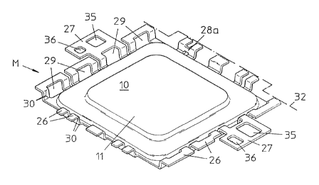
The finished electronic module M shown in figures 5 and
' 6 is now ready for insertion in an injection mould made up of
two halves 44 and 45, as shown in figure 7. At the ends of the
two lugs 27, suitable openings 35 are provided which can be
gripped by the grippers of an assembly robot. Next to these are
centering holes 36 in which centering pins 46 of the injection
mould engage, as shown in figure 7, to ensure that the module M
is accurately positioned for the chip card in the mould's void
K'. Note that this positioning process is performed directly on
the module's external contacts and not indirectly by way of the
module's casing.
Generally, the lugs 27 of the system support 20 that
14
CA 02206786 1997-07-24
project beyond the plastic casing 10 are designed to interact
with automated assembly equipment used for handling the modules
M. The gripper and/or positioning profiles 35, 36 of the modu-
le's metal structure, for example shaped like those shown, lie
in a precise positional relationship to the module's external
contacts 21. This also ensures precise automated manipulation
and accurate positioning of the modules, for example in test
operation, packaging, etc. Use of a metal rather than a plastic
structure and the relatively large offset between the profiles
35, 36 of the two lugs both ensure this high positioning accu-
racy.
A thin decorative film 48 can be laid in the injection
mould 44, 45, as shown in figure 7, against which the electronic
module M then lies with its flat face 12 and external contacts.
The film used for this is usually printed in such a manner as
to be suitable for a thermal transfer printing process, in which
:: :a =rri~~tcu ima~c c:cn~bines only with the plastic injected in the
void K' of the mould, but not with the metal parts of the elec-
tronic module.' The film 48 is used to obtain a printed image on
the face of the chip card by wellknown means. In the upper half
of the mould 45 a label 47 covers the electronic module M. This
is also printed and extends over the whole of the chip card for-
mat. For making the chip card, injection of thermoplastic mate-
rial, preferably ABS, into the void K' of the mould also uses
techniques known per se. In this process, the plastic material
CA 02206786 1997-07-24
is injected all round the edges of the module M, which becomes
perfectly flush with the injected material of the card; the
thermoplastic material passes through the windows 29 and late-
rally between all the lugs 26, 27, and thus forms an extremely
solid mechanical bond between the module's metal parts, espe-
cially its external contacts, and the material of the card. It
is note-worthy however that no thermoplastic material is used
as a backing on either face of the module, i.e. the electronic
module is of the same thickness as the thermoplastic material
of which the card is made. In other words, the full thickness
of the injected card material is available for the module casing
10; thus, for a given card thickness if 0.84 mm and a thickness
of, say, 0.12mm for the label 47, the module casing 10 can be
0.72 mm thick.
The electronic module described above and other suitable
embodiments thereof are also recommended for integration in
other thin, flat plastic objects or supporting bodies, such as
electronic keys. Generally, however, various other forms of in-
tegration and~use are also possible, i.e. wherever a thin, flat
type of module is necessary or offers special advantages, as for
example in the assembly of components on printed circuit boards
by the SMD (surface mounted device) technique.
Figures 8 to 13 show a further embodiment of an elec-
tronic module of extra-thin construction and of its manufacture.
In this case, injection moulding of the module's casing and its
16
CA 02206786 1997-07-24
integration in a card or other supporting body are similar as
described above and not shown separately; cf. figures 4 to 7 and
the related description set forth above. Many of the module's
components in the embodiment of figures 8 to 13 are similar to
those in the embodiment described above and thus have the same
reference numbers.
The following differences apply to the system support
20' in figure 8: On the external contacts 21, the portions re-
mote from the chip pad 22 are not connected to one another by
webs, as items 28 in figure 1, but extend separately into the
lateral margins of the system support 20'. The contacts 21 have
no perforations such as 31 and 29; instead, lateral cutouts 29'
are provided which lie on bending lines 30, as figure 10 indi-
cates. On the bridges 25 that hold the chip pad 22, webs 16
connect the outlying portions to the system support, and slits
17 are provided oil both sides of the webs 16; these slits 17
are parallel to each other and to the contacts 21, and lie on
further bending lines 30, as seen in figure 10.
Figure 9 shows the chip 1 mounted on the system support
20' and connected electrically by leads 3 to the external con-
tacts 21. Chip 1 is again attached to the system support 20' by
an insulating bonding film 2' that lies between them, but in
this embodiment the film 2' extends beyond the area of the chip
1 as far as over the contacts 21, bridges 25, and slits 17. In
particular, the film also covers all the slits 23 and 24 that
17
CA 02206786 2000-12-19
30024-1D
form the boundaries of the chip pad and of the external
contacts. The film 2' is typically made of tape material, such
as polyimide, for example 50~m thick Kapton~ or Mylar°, and has
holes die-cut or punched out before it is applied to the system
support 20', as follows:
- two openings 5 that leave the webs 16 exposed;
- openings 6 for the passage of the wires 3 to the
external contacts;
- a centering hole 7 which is brought in to
coincidence with a corresponding hole 7', as shown in figure 8;
- an edge cut-out in the area of the sprue or stalk
42 that occurs in injection moulding of the module casing 10;
figure 9 shows 42 and 10 dot-dashed;
- if necessary, a hole 9 may be left in the area of
the chip pad for connecting the underside of the chip to the
system support by means of a conductive adhesive.
The thus prepared section of film 2' may be laminated
to the system support 20', as described above for the adhesive
film 2 in connection with figure 2. The chip 1 is then bonded
to the adhesive film and the electrical connections are made,
all similarly as described above.
In the present embodiment, the film 2' not only
provides an elastic mechanical bond between chip and system
support, but also has other functions: the adhesive film
provides an intimate, large-surface connection between the
adjacent contacts
18
CA 02206786 1997-07-24
21, the chip pad 22, and the bridges 25. In injection moulding
of the casing 10 in a mould similar to that described and shown
in figure 4, the film 2' stops the plastic material penetrating
into the slits 23, 24 and under the external contacts 21 on the
module's outer surface, i.e. it prevents the unwanted formation
of so-called flashes on the outer surface. A film material and/
or adhesive coating used with some but slight electrical con-
ductivity may be used for the effective attenuation of voltage
peaks, for example due to electrostatic discharges that reach
the external contacts, to provide so-called ESD protection (ESD
- electrostatic discharge); this is especially important in the
case of chip cards, because the terminals of the integrated
circuit, i.e. the external contacts, are exposed on the outside
of the chip card and are insulated from one another. A further
important function of the film 2' in the area of the slits 17
is explained below in connection ~~~ith figures 11 and 13.
~n ti~i5 second embodiment, the film 2' provides practi-
cally the only, though indirect mechanical link between the
casing 10 and the system support 20'. Experience has shown that
adhesion'of the casing's plastic on the film 2', and of the film
on the system support, is far greater than direct adhesion be-
tween the materials of the casing and of the system support.
Hence the adhesive film 2' considerably strengthens the module
M, and, in particular, it effectively prevents the external
contactslbecoming loose or pulled out from the chip card's sur-
19
CA 02206786 1997-07-24
face. Conversely, after injection moulding of the casing 10, the
sprue or stalk 42, which forms directly on the metallic surface
of the system support, is easy to remove from its metal sub-
strate and to break off at the edge of the casing.
Figure 10 indicates that when the module has been taken
out of the injection mould for making the casing 10, and after
removal of the sprue or stalk, two symmetrical surfaces 14 are
punched out from the system support 20', while the module is
still held by its two webs 16. This cutting-free operation
severs the contacts 21 on the outside, but they still remain
attached to the casing 10 via the adhesive film 2'. The profiles
of the lugs 27 are shaped in the same punching process, and a
hole 35 can be punched out at the same time in the upper lug 27,
the sprue or stalk 42 having been removed. In the same opera-
tion, four lugs 34 are also punched out on both sides of the
two webs 16 near the slits 17.
-im d mexi step, a bending tool bends over the projecting
portions of the system support's metal strip, along the bending
lines 30 on the edges of the module, whereby the webs 16 are
left flat and hold the module attached to the system support.
Finally, a further punching tool also trims off the webs 16 and
thus releases the finished module bi from the system support 20'.
The modules M made in the fully automated manner as
described above and shown in figures 11 to 13 can then be inte-
grated in a chip card or other support by an injection-moulding
CA 02206786 1997-07-24
technique similar to that described earlier by reference to
figure 7 for the first embodiment. As regards reliability of
fixation etc, essentially the same characteristics and features
are obtained. The plastic material of the supporting object is
likewise injected around the edges of the casing 10 and bonds
to the flat surface surrounding the module casing 10, which is
covered by the film 2', and likewise to the bent-over portions
26', 27, and 34, as will be easily recognized from figures 11
to 13.
Finally, figure 13 shows the additional function of the
film 2' which is drawn across the slits 17, as brief reference
has already been made. During injection moulding of a supporting
body or object, such as a chip card, the plastic material pene-
trates into the slits 17 but remains separate along the slits
due to the film 2'. This provides a useful hinge effect along
the slits 17 that can to a large extent cope with the stresses
produced when the card is bent, and thus further protects the
module M and the chip 1 from damage due to excessive bending of
the card. It would also be feasible, if necessary, to use the
same means in respect of the lugs 26' and 27, i.e. by providing
further slits in that areas and extending the film 2' past these
lugs and the zones where they are bent over. In the case of chip
cards, however, because of the established standard layout of
the module M caithin the rectangular card format, the bond be-
tween the lugs 34 and the card's material is subjected to far
21
CA 02206786 1997-07-24
greater bending stresses than the corresponding bond at lugs
26', 27.
22