Note: Descriptions are shown in the official language in which they were submitted.
CA 02207087 1997 - 06 - 0~
WO 97/14142 PCT/IB96/00995
"Optical registration tape"
The invention relates to a method of manufacturing a read-only optical
re~ictr~tion medium in the form of a flexible tape.
The invention also relates to a read-only optical registration medium in the
form of a flexible tape having a layered structure.
The invention further relates to a cassette comprising a housing which
contains such an optical registration tape in combination with two spools, the tape being
partially wound around one of the spools and being connected to the other spool.In an optical registration medium, recorded binary data can be read by
sc~nning a focused light beam along a reflective registration surface of the medium. Each
10 data bit in this registration surface is represented by a localised region having specific
reflection characteristics, which are mutually different for data bits representing a " 1 " and
those representing a "0". For example, in a Compact Disc, data bits are represented by a
series of pits in an otherwise smooth registration surface. The depth of these pits is chosen to
have a value ~/4n, whereby the scanning light beam is assumed to be polarised and to have a
15 monochromatic wavelength ~ (in air), and the registration surface is assumed to be overlaid
by a protective film of refractive index n. As a result, light reflected from a pit-bottom will
demonstrate a path-difference of ~/2n (phase-difference of 7r) with respect to light reflected
from an un-pitted portion of the registration surface. This phase-shift can in turn be detected
on the basis of interference effects. In this manner, it is possible to optically "read" the
20 topography of the registration surface, and thus also the binary bit-streams to which that
topography corresponds.
A method as stated in the opening paragraph is known from German
25 Patent Application DE 35 20 111, in which a screen printing procedure is used to create
small pigmented domains on a reflective registration surface of a tape. The reflection
coefficient of these domains differs significantly from that of the surrounding un-pigmented
surface, so that stored data on the tape can be optically read by monitoring the intensity of
the scanning light beam after its reflection from the registration surface.
CA 02207087 l997-06-0~
W O 97/14142 PCT~B96/00995
In another method of manufacturing an optical registration tape, use can
be made of a so-called phase-change m~tPn~l, which, when locally heated, is capable of
undergoing an irreversible change in crystallographic state (e.g. amorphous to crystalline),
with an ~ttton~l~nt change in reflection coefficient. A layer of such material on a tape-like
5 substrate can be inscribed using a focused laser beam whose intensity is modulated in
accordance with a given binary bit-stream. In analogy to the medium described above,
information can be retrieved from the phase-change layer by monitoring the intensity of a
light beam reflected therefrom.
A further method as specified in the opening paragraph is ~ cussed in an
10 article by D. Pountain in Byte, February 1989, pp 274-280. This method makes use of laser
ablation to blast localised pits in a dye polymer layer which overlies a metallic film on a
tape-like substrate. When a focused light beam is directed onto the pitted dye polymer layer,
a fraction of the light intensity will be reflected immediately from the surface of the layer,
whereas the remaining light intensity will penetrate towards the underlying metallic film,
15 where it too will undergo reflection. The reflected beams from the metallic film and the
pitted surface subsequently interfere with one another, to a degree which depends on whether
the surfacial beam emerged from a pit or from an unpitted portion of the dye polymer layer.
In this manner, the topography of the pitted surface can be optically read.
All of these known methods, and their associated product media, have
20 certain disadvantages. For example:
- In the first medium, the smallest pigmented domains which can be produced
using a screen printing procedure have a typical diameter of the order of 20-50
m. In contrast, the width of the pits on a Compact Disc is of the order of
l~Lm. It is therefore evident that the storage density of such pigmented tape falls
very short of the levels achievable with disc media. In addition, the very nature
of the reading procedure regularly exposes the pigmented domains to intense
laser light, with the attendant long-term risk of pigment fading and associated
increase in noise levels;
- In the case of the second medium, an inherent disadvantage of phase-change
materials is that they must be inscribed in real time, i.e. the speed at which they
are inscribed is of the same order of magnitude as their play-back speed. This is
due to the fact that the localised phase-changed domains must be written on a
one-by-one basis, using a focused laser beam. An additional disadvantage is the
inherent statistical risk of a spontaneous reverse phase-change in some domains.
CA 02207087 l997-06-0~
W O 97/14142 PCT~B96/00995
Though this risk is relatively small, it can nevertheless lead to increased noise
levels in the long run;
- A drawback of the third medium is that the pits produced by laser ablation are
rather ill-de-fined, with an irregular depth and raised rim walls. In addition, the
m~teri~l removed to create the pits in the first place can precipitate as unwanted
debris somewhere else on the me ~ m. Moreover, as in the previous case, the
ablative medium must be inscribed in real time, which is tedious (and costly).
It is an object of the invention to provide an alternative method of
manufacturing a read-only optical registration medium in the form of a flexible tape. In
particular, it is an object of the invention that such a method should circumvent the problems
cited hereabove. Specifically, it is an object of the invention to provide a method with which
it is possible to create well-defined data domains in a registration layer, without problematic
15 precipitation of debris. Moreover, it is an object of the invention that, if so desired, such
domains should have a width of the order of only l~m. In addition, it is an object of the
invention that the new method should allow fast inscription of the said registration layer.
These and other objects are achieved in a method which is characterised
in that it comprises the following steps:
(a) Providing a flexible substrate in the form of a tape;
(b) Providing an embossable registration layer on the substrate;
(c) Embossing the registration layer under pressure with the aid of stamper, so as
to form a pattern of low and high surfacial regions representing a collection ofbinary data;
(d) Providing a protective film over the embossed registration layer.
The inventive method exploits a surprising discovery, as will now be elucidated.Reo~ e a registration tape is inevitably wound around itself during
storage, and generally makes contact with various wheels and capstans during the reading
procedure in a typical play-back device, it is important that the tape should demonstrate a
30 certain surfacial roughness, so as to prevent it from sticking to itself or to other surfaces. On
the other hand, an optical registration tape is preferably optically smooth on the side from
which its registration surface is read. These two requirements are generally reconciled by
ensuring that the side of the tape remote from the registration surface is sufficiently rough. In
analogy to magnetic tapes, such a requirement can be economically achieved by depositing
CA 02207087 l997-06-0~
W O 97/14142 PCT~B96/00995
the registration layer on a substrate material containing so-called fillers, i.e. embedded
microscupic particles. An example of a widely-used substrate material for this purpose is
polyethene terephthalate (PET).
One might regard such rough substrate materials as being incompatible
5 with an embossing procedure, in view of the risk of pressing the substantial substrate
ro~-ghnes~ through to the registration surface during embossing. However, the inventors have
discovered such apprehension to be unfounded, and have shown that, surprisingly, well-
defined micron-sized pits can be successfully embossed in a registration layer overlying a
rough substrate (e.g. a photocurable resin layer deposited directly on a PET substrate foil
containing fillers). The use of a so-called subbing layer (buffer layer) between the substrate
and the registration layer is not essential.
The manifold advantages of the invention are clear. For example, since
data inscription involves embossing with a stamper instead of laser ablation, there are no
problems with precipitated debris on the registration surface, and the embossed forms
(usually pits of constant width but variable length) can be as small and sharply defined as in
the case of a Compact Disc. Moreover, embossing with a stamper allows inscription to occur
at high speed.
According to the inventive method, the stamper itself may, for example,
take the form of a (hard) drum whose cylindrical surface contains microscopic bumps
arranged along a helical path, the width of this path being equal to the width of the tape. If
such a stamper is rolled along the tape's registration layer, in such a manner that the region
of contact between the drum and the tape translates along the said helical path, then the
registration layer will be inscribed with pits corresponding to the said bumps.
In an alternative scenario according to the invention, the stamper takes the
form of a (hard) tape having a master side which is provided with a longitudinal array of
microscopic bumps. If such a stamper tape is wound from one spool to another, and its
master surface is thereby rolled at some point against the registration layer of the optical
tape, which is concurrently being wound between two different spools at the same speed and
in the same direction, then the registration layer will be endowed with pits corresponding to "
the bumps on the master surface.
The flexible substrate employed in the inventive method may be
roughened by the presence of fillers therein (e.g. microscopic silica or alumina particles), or
by the application of a backing layer thereupon. An example of a suitable substrate material
in the first category is LUMIRROR (Toray Industries, Inc.), which is a transparent PET foil
CA 02207087 l997-06-OF7
WO 97/14142 PCT/IB~G/~ U~S
s
having a thicknec~ of approximately 8 ~m and cons~ining fillers with a ~ meter of the order
of 400 nm. On the other hand, a suitable substrate material in the second category is a PET
foil which has been coated on one side with a binder (e.g. a resin) cont~ining dispersed
~ particles of carbon black, chromium trioxide or calcium carbonate (ideally having a ~ eter
S in the range 50-300 nm); the thicknec~ of such a rough backing layer need only be of the
order of 1 ~m.
In a particular embodiment of the method according to the invention, the
embossable registration layer is chosen to comprise a photocurable organic polymeric
m~teri~l, and, during the embossing step (c), the interface of the registration layer with the
stamper is exposed to curing actinic radiation. An example of a suitable material in this
category is SURPHEX (Du Pont), which is a dry UV-curable material available in the form
of thin sheets of standard thickness (in the micron range). Such sheets can be laminated
directly to a substrate foil, e.g. by heating and rolling. As a further example, use can be
made of a dry photocurable resin (e.g. an acrylic ester) which can be applied to a substrate
foil by dissolving it in a volatile solvent and then roller-coating, spraying or brushing the
resulting solution onto the foil.
An alternative embodiment of the inventive method is characterised in that
the embossable registration layer is chosen to comprise a thermoplastic which, in the
embossing step (c), is first thermally softened, and is then allowed to cool and harden after
being impressed upon by the stamper. The employed thermoplastic should have a lower
softening temperature than the substrate material; in this manner, the registration layer can
be softened without untoward softening of the substrate (with the attendant risk of decreasing
the substrate's roughness). Examples of suitable thermoplastics for this purpose are polyvinyl
chlonde and polypropene.
In yet another embodiment of the inventive method, the registration layer
is chemically softened prior to embossing, by applying a chemical solvent to its exposed
surface. Candidate solvents for this purpose include, for example, acetone and isopropanol,
as well as various chloroalkane solutions, ethers and esters, the exact choice depending on
the particular material employed in the registration layer. After it has been embossed, the
softened registration layer is hardened by removing the employed solvent therefrom. This can
be achieved, for example, by heating the registration layer.
The registration layer will generally have a thickness of the order of 1-10
,um, though a thicker or thinner registration layer is also compatible with the inventive
method.
CA 02207087 l997-06-0~
W O 97/14142 PCT~96/00995
The protective film provided in step (d) of the inventive method may be
either inorganic or organic. Suitable inorganic materials such as SiO2, TiO2, AlN, Si3N4,
etc., can be provided by reactive sputter deposition or evaporation, for example. On the
other hand, suitable organic materials such as polyurethane or polyacrylate resins can be
5 provided using roller coating, or a spraying or brushing procedure, for example. The
protective film will typically be of the order of 2-10 ~m thick in the case of an organic film,
and 20-500 nm thick in the case of an inorganic film, but may also be thicker, if so desired.
The exposed surface of the protective film is preferably optically smooth.
As here employed, the term "optically smooth" is intended to indicate an RMS surfacial
10 roughntos~ which is at most 50 nm, preferably not in excess of 20 nm, and ideally no more
than 5 nm. Such a finish is generally achieved automatically, as a result of surface-tension
effects in the protective film during its formation.
A particular embodiment of the method according to the invention is
characterised in that, between steps (c) and (d), a metallic reflection layer is deposited on the
15 embossed surface of the registration layer. Such a reflection layer may comprise a pure metal
or an alloy, and may be provided using sputter deposition, vapour deposition or laser
ablation deposition, for example. Exemplary materials for this purpose include aluminium,
gold, copper, silver, and their alloys. Use of such a reflection layer ensures that, when the
regis~ration side of the medium is scanned with a focused light beam, enough light intensity
20 is reflected to yield an acceptable output signal level.
An alternative embodiment of the inventive method is characterised in that
at least one dye is added to the registration layer and/or the protective film, so as to achieve
a substantial difference between the refractive indices of the registration layer and the
protective film (at the wavelength of the reading light beam). In this manner, it is possible to
25 increase the reflection coefficient at the interface between the protective film and the
registration layer (for light incident through the protective film). In particular, for a sufficient
difference in refractive index, Total Internal Reflection can be induced at this interface, with
a relatively small associated Brewster angle in the protective film. The term "refractive
index" as here employed should be interpreted as referring to the complex refractive index n
30 = n + ik, where n is the real refractive index and k is the absorption coefficient. The
difference between the values of h for the registration layer and the protective film may lie in
either the real or imaginary part of n, or both. In the case of a dye added to the protective
film, however, the value of k for that dye should preferably be relatively small, so as to
avoid untoward absorption of the incoming and reflected light beam.
CA 02207087 1997-06-0~
W O 97/14142 PCT~B96/00995
Examples of suitable dyes as ~liccllssed in the previous paragraph include
pyrylium-4,4'-cyanine and butyl-benzo-indo-carbocyanine. These dyes have res~ec~ e n-
values of 3.270 and 3.050, and le~e~ e k-values of 0.570 and 0.058 (all values at a
wavelength of 780 nm). Alternatively, use can be made of, for example, a squarylium dye.
If required or if so desired, various other layers may be applied between
those provided in steps (a), (b), (c) and (d) of the inventive method. For example:
- An adhesive layer or adhesion-promoting layer may de disposed between the
substrate and the registration layer;
- A dielectric layer may be applied between the registration layer and the
protective film;
- A rough backing layer may be applied to the side of the substrate remote from
the registration layer.
This list is given by way of example only, and is not exhaustive.
The method according to the invention can be employed to manufacture a
15 novel read-only optical registration tape with excellent properties. Such a tape is
characterised in that it has a layered structure which succçccively comprises:
- A substrate;
- A registration layer;
- A reflective registration surface, in which binary data are represented by
localised level-variations, and
- A transparent, optically-smooth protective film,
that there is no metallic reflection layer between the substrate and the registration layer, and
that the side of the substrate remote from the registration layer is rougher than the exposed
surface of the protective film.
The "reflective registration surface" referred to hereabove may be
interpreted as being one of the following:
- A metallic reflection layer, applied to the side of the inscribed registration layer
remote from the substrate;
- The interface of the inscribed registration layer and the protective film, if use
has been made of a dye to enhance the reflection coefficient at this interface.
The "localised level variations" may, for example, be achieved by endowing the registration
layer with a pattern of pits or bumps. For example, along any given path, a " 1 " may be
rel),esellted by a pit, whereas a "0" may be represented by a level (i.e. unpitted) portion of
the surface S in which the pits are made, the length of such a pit or level portion being an
CA 02207087 l997-06-0~
W O 97/14142 PCT~B96/00995
integral multiple of some basic unit lepl~senting a single bit. Both the surface S and the
bottom of each pit are reflective, and reading of the registration surface can be achieved on
the basis of the phase-difference between a (polarised) light beam refl~ted from the surface
S and one reflected from the bottom of a pit. For this reason, the magnitude of the level
S differences in the registration surface is preferably )~/4n, for (polarised) light of wavelength
and a plul~;li~/e film of real refractive index n.
Various other layers may also be incorporated in the layered structure of
the inventive medium (as already discussed above). These include, for example, adhesive
layers, adhesion-promoting layers, dielectric layers, b~.king layers, etc.
The invention also relates to a cassette comprising a housing which
contains two spools and the inventive read-only optical registration tape, the tape being
partially wound around (at least) one of the spools and being connected to the other spool. In
a particular embodiment of such a c~ccett~, the tape passes from one spool to another via
guiding means which serve to position the tape behind an aperture in the housing in such a
15 manner as to allow in situ optical access through the aperture to the registration surface of
the tape. However, such guiding means are not strictly necessary: if so desired, the tape can
be looped out of the cassette housing and can be read ex situ.
The invention and its attendant advantages will be further elucidated with
the aid of exemplary embodiments and the accompanying schematic drawings, not all of
uniform scale, whereby:
Figure 1 renders a cross-sectional view of a flexible substrate in the form
of a tape, on which an embossable registration layer has been provided;
Figure 2 shows the subject of Figure 1 subsequent to the performance of
an embossing step thereupon, resulting in the formation of a pattern of low and high surfacial
regions in the registration layer;
Figure 3 depicts the subject of Figure 2 subsequent to the provision of a
metallic reflection layer on the embossed registration layer;
Figure 4 shows the subject of Figure 3 subsequent to the provision of a
protective film over the metallic reflection layer, thereby creating an optical registration tape
in accordance with the invention;
Figure 5 depicts manufacturing apparatus for enacting a particular
embodiment of the inventive method;
CA 02207087 1997-06-0~
W O 97/14142 PCT~ 95
Figure 6 shows a cassette in accordance with the invention.
Embodiment 1
s
Figures 1-4 depict various stages of a particular embodiment of the
method according to the invention, and also of a particular embodiment of the inventive
optical registration tape. Collcs~onding features in the various Figures are denoted by the
same reference symbols.
Figure 1 renders a cross-sectional view of part of a flexible substrate 1 in
the form of a tape. The substrate 1 has two major surfaces la, lb, and is approximately 8
~m thick. It contains embedded microscopic fillers (not depicted), whose presence causes the
surfaces la, lb to demonstrate an RMS roughness of the order of 10-20 nm. An example of
a suitable such substrate 1 is a transparent PET foil in which silica particles having a
15 diameter of the order of 400 nm have been dispersed. Such a substrate 1 is commercially
marketed under the brand name LUMIRROR (type N997) by Toray Industries, Inc.
An embossable registration layer 3 has been provided on the surface lb of
the substrate 1. This layer 3 has a thickness of the order of 10 ~m, and comprises, for
example, a dry photocurable resin. In this particular embodiment, the employed resin is
20 SURPHEX P-6 (marketed by Du Pont), which is available in sheet form at a thickness of 6
~m, and was directly laminated onto the substrate I at a temperature of 120 ~C and a rolling
pressure of 250 kPa. The layer 3 presents a surface S remote from the substrate 1.
In Figure 2, the layer 3 has been embossed under pressure with the aid of
a stamper (not depicted), in accordance with the inventive method. In this particular
25 embodiment, this has entailed the creation of shallow pits 5 in the surface S. The pits 5 have
a depth of approximately 150 nm, a width (perpendicular to the plane of the drawing) of
approximately 0.5 ~Lm, and variable length. A suitable embossing procedure is described in
Embodiment 2 herebelow.
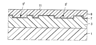
In Figure 3, the embossed surface of the layer 3 has been coated with a
30 thin metallic reflection layer 7. In this case, the layer 7 is comprised of Al, has a thickness
of 100 nm, and has been deposited using Vacuum Vapour Deposition. Rec~use it hugs the
contours of the original embossed surface of the registration layer 3, the layer reflection 7
demonstrates a series of sharply defined pits 5' in an otherwise smooth exposed surface.
Figure 4 shows the subject of Figure 3 after the provision thereupon of a
CA 02207087 l997-06-0~
W O 97/14142 PCT~B96/00995
~ruLe~ /e film 9. The material of the film 9 is, in this case, a polyacrylate resin, and has
been roll-coated onto the reflection layer 7 to a thickness of approximately 5 ~Lm. The
exposed surface 11 of the film 9 is optically smooth, with an RMS roughne~c of S nm. This
finish is naturally achieved as a result of surface tension effects in the film 9 during its t
formation on the underlying reflection layer 7.
Embodiment 2
Figure 5 depicts manufacturing apparatus for enacting a particular
embodiment of the inventive method. The employed stamper 51 has the form of a cylindrical
aluminium drum with a diameter of 150 mm and a length of 165 mm, and with a relief
pattern of microscopic bumps on its cylindrical surface 51a. The manner in which such
bumps can be created is discussed in Embodiment 3 herebelow.
Also depicted in the Figure is a roller 53 of similar diameter to the drum
51 but having a hard paper layer of thickness 5 mm on its cylindrical surface 53a. The drum
51 and roller 53 are arranged with their cylindrical axes parallel to one another, and with
their cylindrical surfaces 51a, 53a pressed against opposite sides of an interposed optical
registration tape 55, which is as yet unembossed. This tape 55 extends substantially
20 perpendicular to the said cylindrical axes, in such a manner that its (curable) registration
layer is in contact with the relief pattern on the surface 51a.
The drum 51 is pressed against the roller 53 with a force of 5000 N,
resulting is a pressure of the order of 15 N/mm2 on the tape 55. By rolling the drum 51 and
roller 53 against one another, the interposed tape 55 is pulled through between them, and its
25 registration layer is embossed along its length with a series of pits corresponding to the
bumps on surface 51a.
The registration layer on the tape 55a is cured by directing actinic
radiation R (e.g. UV radiation) onto that region 55a of the tape 55 which, at any given time,
is still in contact with the surface 51a. If so desired, supplementary curing can be
30 subsequently performed using a second beam of actinic radiation R'.
Once curing has been performed, the tape 55 passes through an on-line
deposition chamber 57, where the embossed surface of the tape 55 is provided with a
vacuum-evaporated metallic reflection layer. In an alternative scenario, the tape 55 is first
wound onto a buffer spool A, which can later be transferred into a vacuum chamber; the tape
CA 02207087 l997-06-0~
W O 97/14142 PCT~B~G~5
11
55 is then unwound from the spool A and met~ ed on its embossed side.
The tape 55 is subsequently provided with a ylvtecLi~e film on its
embossed side. This is here achieved by roller-coating the tape 55 in a roller-coater S9. If
required, the freshly coated tape 55 may be subsequently dried using a heat source or air
flow H. ~ltern~tively, if the applied resinous liquid is photocurable, then the means H can be
regarded as comprising actinic radiation for the purposes of curing the freshly applied film.
In a further process step, the tape 55 is either wound onto a buffer spool
B, or is directly wound into a ç~sette housing Sll. If required, the tape 55 may first be cut
to an ayyl~,y~iate (uniform) lateral width (e.g. 8 mm) with the aid of cutting wheels 513.
Embodiment 3
The microscopic bumps on the cylindrical surface Sla of the stamper
lS drum 51 can be created using either a direct or indirect procedure, as will now be explained.
In a suitable direct procedure, the cylindrical surface Sla is coated with a
layer of photoresist. Using an apl)lol,liate interposed mask, this layer of photoresist is
irradiated in accordance with the desired surfacial pattern of bumps, and is subsequently
developed and cross-linked.
In an appropriate indirect procedure, the process described in the
prece~iing paragraph is performed on one side of a sheet or ribbon, which is then wound
around the drum 51 in such a manner that the bumped side of the sheet or ribbon faces
outward and forms the surface 51a.
Embodiment 4
Figure 6 depicts a particular embodiment of a c~c~ette 60 in accordance
with the invention, comprising a housing 62 which contains two spools 64 and a read-only
optical registration tape 66 according to the invention. Also depicted is an aperture 68 in a
wall of the housing 62. The tape 66 can be wound back and forth from one spool 64 to the
other, and is thus arranged that its registration surface faces the aperture 68. In this manner,
the reflective registration surface of the tape 66 can be ~cce~sed in situ by a light beam
entering and leaving the housing 62 through the aperture 68. In order to facilitate accurate
CA 02207087 1997-06-0~
W O 97/14142 PCT~B9G/~G995
12
focusing of such a light beam on the tape 66, the housing 62 may also contain guide means
(not depicted), which serve to maintain a given length of the tape 66 at a constant t~ nce
from the aperture 68. Such guide means may, for example, comprise a reference block over
which the tape is sp~nned and which is located behind the aperture 68.
In an alternative embodiment of the inventive cassette 60, the guide means
crcl.cd to hereabove may be omitted from the housing 62, and the tape 66 may be read
using a play-back device which loops a given length of the tape 66 out through the aperture
68 and then reads it ex silu, in analogy to a VHS video cassette, for example. For such
purposes, the aperture 68 is preferably much wider than here depicted, so as to facilitate
10 mechanical access to the tape 66.
In both of these embodiments, the aperture 68 is preferably located behind
a mechanical shutter door (not depicted), so as to protect the tape 66 from dust and
scratches.