Note: Descriptions are shown in the official language in which they were submitted.
CA 02207285 1997-06-06
WO 96118197 PCT/US95/14591
Force Sensing Ink, Method Of
Making Same And Improved Force Sensor
Background Of The Invention
For some time now a variety of techniques have
~ 5 been used to fabricate force sensors which provide an
indication of the force applied between a pair of mating
surfaces. These techniques have included the utilization
of thin layers of semi-conductive materials disposed
between the surfaces which respond to applied loads and
which, when properly provided with conductors and
associated circuitry, facilitate the display of
indications of applied loads.
Early versions of products employing some of
those features include those disclosed in U.S. Pat. Nos.
3,806,471 and 4,489,302. The common characteristic of
those products is that they employ a body of semi-
conductive material which, when stressed by the
application of a load, will increase in conductivity.
That increase in conductivity, which tends to increase as
a function of the applied load, may then be used to
provide a measurable output which varies, within limits,
as a function of the applied load. Force sensing systems
employing semi-conductive materials and based upon these
principles are additionally shown by U.S. Pat. Number
4,856,993.
Typically semi-conductive layers used in force
sensors must have certain characteristics to be
sufficiently electrically conductive to be effective.
Thus such layers must have electrically conductive areas
which are close enough together to allow conduction under
load. Under load the conductive areas must contact each
other or the distances between them must be so small that
A
electrons can flow from one conductive area to the next.
The concentration of conductive areas must be large
enough to provide a conductive path through the layer.
The conductivity through the layer must be sufficient,
CA 02207285 1997-06-06
WO 96/18197
PCT/U~95/14591
under load,[to provide a reliable and consistent range of
different resistances (or conductances) to be able to
distinguish among a range of applied loads. Typically '
the application of a load increases the capacity of the
layer to allow electron transfer. Further, the '
conductivity changes should be reversible to the extent
that the layer and surf aces on which the layer is applied
permit restoration of the characteristics of the layer
which are altered as load is applied. The pressure-
sensitive, load responsive characteristics may be at the
surf ace of the layer or internally thereof, or both.
A variety of intrinsically semi-conductive
materials have been used to provide force sensors of this
type. Such materials include particulate molybdenum
disulfide, and ferrous and f°_rric oxide, among others.
Such materials are disclosed in the patents referred to
above, as well as in U.S. Pat. No. 5,296,837.
In addition to the use of semi-conductive
systems to produce force sensing transducers, particulate
conductive materials have also been used to produce force
sensing transducers, as exemplified by the disclosure of
U.S. Pat. No. x,302,936. This patent and U.S. Pat. No.
5,296,837 both disclose the use of carbon as a conductive
material in force sensing inks. The latter patent uses
stannous oxide as a semi-cenduct~.ve material in
combination with carbon.
In more recent Mmes, as shown by the prior art
referred to above, semi-conductive, pressure-sensitive
transducers have been made by depositing semi-conductive
material, as it the form of an "ink" deposited by
spraying or by a silk screening process, to form a thin
layer or layers between a pair of electrodes. Typically,
the electrodes are disposed on thin, rlexible plastic
sheets and have leads to a remote region in which the
flow of an applied csrrent may be sensed and measured.
-2-
~SItfQIE ~f~EET (~iR~ ~
CA 02207285 1997-06-06
WO 96/18197 PCT/US95/14591
In such sensors, the electrodes and dried ink residue
form a sandwich which acts as a force transducer, and
which will provide a variable resistance (or conductance)
' which is related in a predetermined manner, to applied
loads.
' The prior art also teaches the use of blends of
semi-conductive particles and conductive particles to
provide a variably conductive force transducer. In
particular, the prior art teaches the use of molybdenum
disulfide as a semi-conductor blended with graphite or
finely divided conductive carbon (such as acetylene
black). The conductivity of inks based on these
materials may be varied by the concentrations or ratios
of the conductive and semi-conductive particles,
frequently by blending a highly conductive ink with a
less conductive ink. Polyester is the binder frequently
used to bind the particles in these inks to a substrate
on which a dried layer of the deposited materials is
disposed. The resistance of the dried layer varies with
load; hence these inks are referred to as being pressure-
sensitive or force-sensitive.
These prior art inks have a number of
shortcomings. For example, conventional binders, such as
polyester binders, limit the useful application
temperatures to a range of from up to 120 to no more than
about 150F. Above that temperature range, binders in
confronting semi-conductive layers tend to bond to each
other. Further, conductive carbon black when used as a
pigment in resistive inks is very difficult to disperse
uniformly and tends to agglomerate after dispersion. In
addition its surface reactivity and adsorption
characteristics significantly depend on processing
variables and heat history. Further, graphite platelet
orientation in the dried ink film is difficult to
reproduce from sensor to sensor. These factors add great
-3-
CA 02207285 1997-06-06
WO 96/18197 PCT/US95/14591
variability to the conductivity of such inks, hence cause
unacceptable and undesirable variations within a product
and from product to product.
Because molybdenum disulfide becomes more
conductive as temperature increases, the use of
molybdenum disulfide and conductive carbon black to
provide the conductive paths requires changing their
ratios or concentrations to adjust the conductivity of
the ink for anticipated temperature conditions to be
encountered. Because of the sensitivity of molybdenum
disulfide to changes in temperature, compensation for
temperature is difficult when the concentration of
molybdenum disulfide is used by itself to adjust
conductivity.
It would be desirable to provide a force
transducer having improved force sensitivity,
reliability, and reproduceability, as well as the
additional capacity to function effectively not only at
current temperatures at which force sensors are used, but
at elevated temperatures, such as at temperatures of from
at least 120°F to 150°F up to about 350°F, while
providing
sufficient sensitivity and reproduceability to provide a
reliable and consistent indication of applied load.
guam~a~ of the Invention
In accordance with the present invention
improved high temperature, carbon-free force sensing
inks, methods of making them and resulting force sensors
are provided. A high-temperature, carbon-free force
sensing ink in accordance with this invention is adapted
to be deposited in a thin layer between a pair of
conductors, each conductor being disposed on a support
surface, the thin layer having a resistance which varies
as a function of the force applied thereagainst, the thin
layer being usable in force sensing applications at
temperatures of from 150° to 350°F and wherein the ink
-4-
CA 02207285 1997-06-06
WO 96/18197 PCT/US95/14591
comprises a high temperature binder, intrinsically semi-
conductive particles, and conductive particles, the
conductive particles preferably comprising a conductive
metal oxide compound that deviates from stoichiometry
based on an oxygen value of two. Preferably the con-
' ductive oxide particles are conductive tin oxide
particles, Fe304 iron oxide particles or mixtures thereof.
The force sensing ink may include dielectric
particles, such as silica having a particle size of 10
microns or less. The semi-conductive particles are
preferably molybdenum disulfide particles. The particles
in the ink are desirably of a particle size of 10 microns
or less (and most preferably no more than about 1 micron
in average size) and the high temperature binder is a
thermoplastic polyimide resin. In a preferred form, the
conductive and semi-conductive particles are present in
a
combined concentration of from at least 20% by volume to
80% by volume of the dried ink when deposited in a thin
layer, and the binder is present in a combined amount of
from 20 to 80% by volume.
In another aspect of the invention, a method of
controlling the temperature and pressure responsiveness
of a carbon-free, pressure sensitive, force sensing ink
layer is provided. It comprises the steps of providing a
first mixture of intrinsically semi-conductive particles
and conductive particles in a ratio of from 15 to 65
parts of semi-conductive particles to 55 parts to 5 parts
of conductive particles by volume, the remainder being a
temperature resistant binder, providing a second mixture
of intrinsically semi-conductive particles and dielectric
particles in a ratio of from 15 parts to 65 parts of
semi-conductive particles to 55 parts to 5 of dielectric
particles by volume, the remainder being a temperature
resistant binder, mixing cruantities of said first and
second mixtures having the same amounts of semi-
-5-
CA 02207285 1997-06-06
WO 96/18197 PCT/US95/14591
conductive particles by volume to produce a force sensing
particulate in a ratio of from 4 to 96's of the first
mixture with from 96 to 4's of the second mixture thereby
to provide an ink for deposit and use in a force sensor.
Preferably the semi-conductive particles are
molybdenum disulfide particles and the semi-conductive
and conductive particles are of an average size of 1.0
micron or less. Desirably the binder is a thermoplastic
polyimide binder and the conductive and semi-conductive
particles are present in an amount of at least 20o by
volume and less than 80% by volume of the dried ink when
deposited in a thin layer. In a most preferred form, the
binder in present in a combined amount of from 20 to 80%
by volume and the conductive and semi-conductive
particles are present in a combined amount of from 80 to
20o by volume.
The resulting pressure-sensitive force sensor
of the present invention comprises a thin, flexible film,
a first electrode on the film, a carbon-free, pressure
sensitive, resistive material deposited on the electrode,
the material comprising a high temperature resistant
binder, intrinsically semi-conductive particles and
conductive particles comprising in the most preferred
form, a conductive tin oxide, Fe,O4ferric oxide or
mixtures thereof, the conductive and semi-conductive
particles being present in an amount of from 20 to 80o by
volume of the material, and a second electrode spaced
from the first electrode by the pressure sensitive,
resistive material so that the material may be saueezed
between the electrodes to vary the flow of current
therethrough as a function of the force applied.
Desirably the material further comprises
dielectric particles, the semi-conductive particles are
articles, and the semi-conductive
molybdenum disulfide p
and conductive particles are of an average size of 1.0
-6-
CA 02207285 1997-06-06
WO 96/18197 PCT/US95/14591
micron or less. Preferably the binder is a thermoniastic
polyimide binder. In a most preferred form, the binder
in present in a combined amount of from 20 to 80% by
_
,, volume and the conductive and semi-conductive particles
are present in a combined amount of from 80 to 20% by
volume when deposited in a thin layer.
Further objects, features and advantages of the
present invention will become apparent from the following
description and drawings.
Brief Description Of The Drawings:
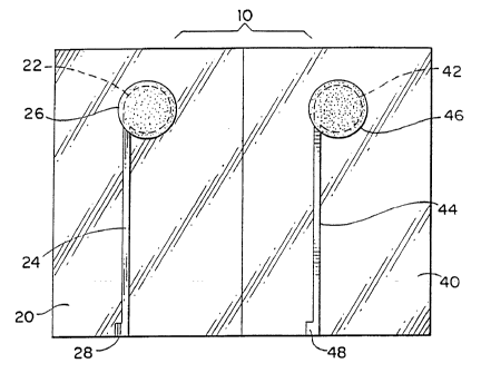
Fig. 1 is a plan view of a pair of sensor
elements which are assemblable to provide a sensor in
accordance With this invention;
Fig. 2 is a plan view of a sensor as assembled
from the el ements of Fig. 1;
Fig. 3 is a graph illustrating the load sensing
characteristics of a force sensor made in accordance with
the present invention; and
Fig. 4 is a graph illustrating the load sensing
characteristics of a further force sensor made in
accordance with the present invention.
Detailed Description
In accordance with the present invention, inks
are prepared which, when deposited, produce intrinsically
semi-conductive layers which are stable and usable at
customary temperatures as well as at temperatures of from
about 120F to 150F up to 350F and which reliably
reproduce responses to forces of as much as 10,000 psi at
350F, even after repeated loading or prolonged exposure
to elevated temperatures and loads.
A high-temperature resistant force sensor
employing inks of the present invention is illustrated in
Figs. 1 and 2. As there is shown, a button sensor 10
comprises a pair of thin, flexible films 20, 40 which may
be transparent. Films 20, 40 may be separate or may be
CA 02207285 1997-06-06
WO 96!18197 PCTriJS95114591
the same sheet which is adapted to be folded into a
sandwich array to produce the sensor 10. Polyester or
polyimide films are preferred. Such films may be ICI
polyester film and DuPont Kapton polyimide film. ICI
polyester film is available from ICI. Americas Inc.,
Concord Pike, New Murphy Road, Wilmington, DE 19897.
Films 20, 40 are provided with electrodes 22, 42,
respectively, which are electrically connected to
conductors 24, 44, respectively, and contacts 28, 48.
The electrodes, conductors and contacts may be deposited,
as by silk-screening a conductive silver ink, in a known
manner, or by sputter coating a layer of copper with an
overcoat of nickel, such as to a total thickness of 2400
angstroms. The conductors are adapted to be connected in
an electrical circuit in a manner known to the art so
that current flow through the sensor 10 may determined in
use. The electrodes may be of any desired shape. In
this case they are shown as being round. Each has a
diameter of 0.5 inch.
Each of the electrodes is overlaid with a layer
26, 46 of carbon-free, pressure-sensitive resistive
material of a diameter of 9/16 inch which is the dried
residue of an ink which was deposited thereon. Such an
ink may be deposited via silk screening, spraying or
other known application techniques. In a preferred form,
that material comprises a high-temperature resistant
binder, semi-conductive particles, such as molybdenum
disulfide or ferric or ferrous oxide particles, arid
conductive particles comprising a conductive metal oxide
compound that deviates from stoichiometry, such as the
reaction product of stannic oxide and antimony oxide,
Fe304 iron oxide, or mixtures thereof. A layer is
preferably formed over each of the electrodes 22, 42 in a ,
diameter slightly greater than the area of the electrode,
so that when a sensor sandwich is formed from films 20,
-g_
CA 02207285 1997-06-06
WO 96/18197 PCT/US95/14591
40 there are~two thin layers o~ pressure-sensitive
resistive material in contact with each other, and which
layers entirely overlay the electrodes, thereby to assure
that the desired contact area is uniform from sensor to
sensor.
In a preferred form, the thin film sensor 10 is
from about 2.5 to about 3.5 mils thick in the sensing
area. The films 20, 40 are each about 1 mil thick, the
electrodes 22, 42 are each about 0.2 to 0.3 mil thick,
and each dried resistive ink layer is about 0.3 to about
0.5 mil thick. Other thicknesses of the elements of the
sensor 10 can be used depending upon the application and
other factors relevant to a particular application, all
as is well understood by those working in the art.
In one preferred form of the practice of the
present invention a high-temperature, carbon-free force
sensing ink adapted to be deposited in a thin layer
between a pair of conductors was prepared as follows.
Example I
First, a 20 percent solution of thermoplastic
polyimide resin was prepared by dissolving the polyimide
in acetophenone. The particular polyimide used was
Matrimide 5218, available from Ciby-Geigy Corporation,
Three Skyline Drive, Hawthorne, New York 10532.
Matrimide 5218 is a fully imidized soluble thermoplastic
resin based on 5(6)-amino-1-(4' aminophenyl)-1,3,-
trimethylindane. To 30 grams of this solution, 10.6
grams of molybdenum disulfide (technical fine grade) and
2.6 grams of the reaction product of stannic oxide and
antimony oxide (sometimes referred to as a conductive tin
oxide) were added. The reaction product used had an
average particle size of 0.4 micron and is available from
Magnesium Elektron, Inc., 500 Point Breeze Road,
Flemington N.J. 08822 under the trade name CP40W. The
reacting material are primarily tin oxide (as Sn02),
-9-
CA 02207285 1997-06-06
WO 96/18197 PCT/US95/14591
namely 90 to 99%, with a minor amount of antimony oxide
- (as Sb~03), namely 1 to 10%. The semi-conductive
molybdenum disulfide and the conductive tin oxide
reaction product particles had an average particle size
of 0.7 and 0.4 micron, respectively.
The polyimide solution and added particles were
mixed in a high speed laboratory mixer for ten minutes.
The resulting ink was then silk screened in a
conventional manner onto each of two circular conductors
(approximately one-half inch diameter) and dried for 15
minutes at 275°F, at which time the acetophenone was
completely driven off. The two layers of pressure-
sensitive resistive material were placed in confronting
contact in a conventional manner and the sensor thus
formed was positioned between a pair of mating surfaces
and placed under load. The results of testing under load
are shown in Fig. 3 which illustrates, for temperatures
of 250°F and 350°F, the resistances in Kohms at the loads
indicated.
Example II
As another example of the practice of the
present 'invention, a 20% solution of Matrimide polyimide
resin was prepared as described above. To 30 grams of
this solution was added 10.6 grams of molybdenum
disulfide and 2.6 grams of conductive iron oxide (as
Fe304). After mixing, depositing and drying in the manner
described in Example I, and juxtaposing the semi-
conductive layers, the sensor thus formed was positioned
between a pair of surfaces and placed under load. The
results of the testing under load are shown in Fig. 4
which illustrates, for temperatures of 250°F and 350°F,
the resistance in Kohms at the loads indicated.
As may be seen from each of Figs. 3 and 4 at
both temperatures of 250°F and 350°F, and at loads of from
200 to 3000 psi, the sensors produced will satisfactorily
-10-
CA 02207285 1997-06-06
WO 96/18197 PCT/US95/14591
- discriminate the loading to whit'.~_ such sensors are
exposed.
~'xamtle ='T
Other carbon-free formulations of Force sensing
inks were made in accordance with the present invention.
Each was found to have superior pressure-sensitive
sensing characteristics at elevated temperatures. '='hese
formulations resulted prom mixing moieties cf Mixtures A
and B. The solvent used i.~.~. each ~oiety was acetophenone
whicz completely evaporates after the ink is deposited.
Thus the formulations are based cn the compositions of
the dried layer.
Mixture A consisted of:
Amo~~nt Bv Weight Bv Volume
Molybdenum Disulfide 85 grams 53.08 27.71
(technical ~=ne)
Conductive Tin Oxide 25 crams 15.64 5.71
Matrimide 5218 50 grams 31.28 66.58
100.00 100.00
A typical Mixture A would use 260 crams acetcphenone as a
solvent.
Mixture B consisted of:
0
Amount Bv Weicht By Volume
Molybdenum disulfide 50 crams 45.12 19.56
(technical t_ne)
Minusil 5 25 crams 17.29 13.86
Matrimide ~2i8 50 crams 37.59 66.58
100.00 100.00
A typical Mixture B would use 260 grams of acetophenone
as a solvent. Minusil 5 is a crystalline silica (SiOZ)
available from U.S. Silica, _.O. Sox 187, Berksley
Springs, West Virginia 25111.
Carbon-free formulations comprising mixtures of
moieties of Mixture A and Mixture B were prepared as set
forth in Table 1. Each was found to have superior
pressure-sensitive sensing characteristics.
CA 02207285 1997-06-06
WO 96/18197 PCT/US95/14591
Table I
Amounts Bv Volume*
Mixture A 20m1 30m1 40m1 50m1 55m1 57.5m1 ,
Mixture B 40m1 30m1 20m1 lOml 5m1 2.5m1
Total 60m1 60m1 60m1 60m1 60m1 60.Om1
* All formulations in Table I have identical ratios of
particulate material to Matrimide 5218 by volume.
It is also to be understood that as the ratio
of Mixture A to Mixture B increases, the ink layer
becomes more conductive because the layer contains more
conductive and semi-conductive particulates.
The force sensing ink system of the present
invention is capable of sensing forces of up to 10,000
psi or more at temperaLUres of up to 350°F. The basic
formulation of high temperature binder, semi-conductive
particles and conductive particles may be supplemented or
modified by changes in ratios and, as indicated, by
incorporation of a dielectric particulate material, such
as silica, thereby to optimize the responsiveness and
sensitivity of the sensor for a given range of
anticipated loads at anticipated operational temperatures
for a particular load sensing application. Although the
dielectric particulate tends to reduce the conductivity
of the ink somewhat, it tends also to improve uniformity
and repeatability of the ink layer resistance.
Preferred compositions in accordance with the
present invention usually fall within the following
ratios of components by volume. The sum of all
components will equal one.
0 of Volume
High temperature binder 20 to 80
Semi-Conductive particles 15 to 50
Conductive particles 5 to 50
Dielectric particles 4 to 50
-12-
CA 02207285 1997-06-06
WO 96118197 PCTlUS95/14591
In pref erred compositions Mixture A contains a
ratio of 15 to 65 parts of semi-conductive particles and
55 to 5 parts of conductive particles by volume and
Mixture B contains a ratio of 15 to 65 parts of semi-
s conduct=ve particles and 55 to 5 parts of dielectric
particles by volume, the remainder being the high
temperature resistant binder. The admixture of Mixtures
A and B is usually in a ratio of from 4 to 96 parts to 96
to 4 parts of contained particulate by volume.
The total concentration of conductive and semi-
conductive particles should eaual at least 20% by volume
of the dried ink layer. That is because for the dried
ink f-lms to be conductive, there must be sufficient
semi-conductive or conductive (or both? particles and
.5 they must be close enough together to allow electrical
conduction and to obtain a conducting pathway trough the
layer. =or a given particle size or distribution, the
number cf particles per unit volume is directly related
to the number of conducting pathways in the ink. The
upper limit of the particulate is approximately 80% by
volume, and will depend upon adhesion and ~'_exibility
requirements of the dried ink layer. The thickness of
the dried ink layer will be dictated in part by the
environment in which the sensor is to be used, and the
reauired flexibility and adhesion parameters.
The median particle size of the conducive,
semi-conductive and dielectric particles should be less
than 10 microns, and pre=erably no more than 1.0 micron
in average size. Where possible, as is apparent prom the
foregoing, the particle size of the consti~uents should
average no more than 1.0 micron in size.
As is known, most conductive and semi-
conduct=ve materials become more conductive as
temperature increases. Changes are not linear. Neither
is the coefficient of resistance change a constant with
-13-
CA 02207285 1997-06-06
WO 96/18197 PCT/US95114591
temperature. Indeed, the curve of resistance versus
temperature or pressure is parabolic. All of these make
clear why as temperatures increase, pressure-sensitive
force sensing layers tend to become less discriminating
and less resistive.
By blending, mixing, and balancing in
accordance with the present invention, greater
sensitivity and reproduceability, especially at higher
temperatures and pressures, can be obtained over both
broad and narrow ranges as compared to those available
with presently available systems and inks.
Tests were conducted to ascertain the
reliability of inks prepared in accordance with the
present invention. To that end a 16% solution of
Matrimide 5218 in acetophenone was prepared and was mixed
with 23.5 grams of technical fine grade molybdenum
disulfide (0.7 micron), 4 grams of conductive tin oxide
(0.4 micron) and 4 grams of ground silica (1.0 micron) in
a laboratory mixer at high speed to produce inks. Button
sensors as described above were prepared by silk-screen
deposition of the inks using a 280 mesh screen.
Using the mixing protocols indicated,
resistances in (Kohms) at 3000 psi (at 350°F) were
obtained, all as indicated in Table II.
Tab- le I I
Mixina Protocol Sensor 1 Sensor 2 Sensor 3
High Speed Mixing-15 Min. 3.37 3.80 3.55
High Speed Mixing-15 Min.,
then aged 24 hours and 4.05 3.78 3.90
mixed'by hand with a
spatula
High Speed Mixing-15 Min., ----
then aged 6 months and 3.78 3.65
mixed by handwith a
spatula
-14-
CA 02207285 1997-06-06
WO 96/18197 PCT/US95/14591
Tests were theft conduced with carbon black as
a conductive pigment. The results of these tests showed
that the inks of the present invention produced sensors
' which were superior in auality and reliability to those
produced using conductive carbon black. The carbon black
tests also confirm that carbon black is very difficult
to
mix into a liquid carrier and to separate and disperse
into its ultimate particle size.
To that end 20% solutions employing Matrimide
5218 in acetophenone were mixed with 13.2 grams of
technical fine grade semi-conductive molybdenum disulfide
(0.7 micron maximum particle size) and 4.32 grams of
conductive carbon black (Shawingen acetylene black which
is available from Chevron Chemical Co., P.O. Box 3788,
Houston Texas 77253). Button sensors as described above
were prepared by silk-screen deposition of the inks using
a 280 mesh screen. The inks were dried for 15 minutes at
275F.
Using the mixing protocols indicated,
resistances (in Kohms) at 3000 psi (at 350F) were
obtained, all as indicated in Table III.
Table TII
Mixiner Protocol Sensor 1 Sensor 2 Sensor 3
High Speed Mixing-15 Min. 0.41 4.2 20.9
High Speed Mixing-30 Min. 3.75 5.1 5.23
High Speed Mixing-60 Min. 3.92 4.15 3.75
High Speed Mixing-60 1.09 4.08 12.0
Min., then aged one week
and mixed with wide
wooden stick
The last test of well mixed material aged one
week demonstrated that pigments had settled and
agglomerated, which is typical of conductive carbon black
based inks. This data, as well as the results of testing
of well-mixed, promptly applied inks incorporating carbon
-15-
CA 02207285 1997-06-06
WO 96/18197 PCT/US95/14591
black, shows that reliability and repraduceability of
results of applied carbon black based inks are so
variable and erratic that such inks are not acceptable
for use in force sensors.
From the foregoing it will be apparent to those
skilled in the art that modifications may be made without
departing from the spirit and scope of the invention. As
such it is intended that the invention is to be limited
only as may be made necessary by the claims appended
hereto.
-16-