Note: Descriptions are shown in the official language in which they were submitted.
CA 02207337 1997-06-23
- A CMOS Integrated Radon Detector
This invention relates to an integrated radon detector, and in particular to a low cost
single chip CMOS integrated radon detector manufacturable using typical commercial
CMOS technologies for use in continuous real-time monitoring of radon.
There has been a growing interest in developing simple, low-cost monitoring
techniques for radon (222Rn) gas which is known to play a significant role in induction of
lung cancer in humans. It has been estimated on the basis of a fairly extensive national
survey, that there are approximately 5 to 6 million homes in the U.S. for which the average
indoor radon concentration exceeds the Environmental Protection Agency's (EPA)
recommended guideline of 4 pCi/L.
Prior work has been performed in developing radon detectors with discrete circuit
components. Although considerable work has been done to improve accuracy in the
measurement of alpha particles produced in the decay of radon and its (1~1lghtP~r products
using special electro-static collectors, as developed by Bigu et al, and described in Rev. Sci.
Instrum, vol 56, no. 1, pp 146-153, Jan 1985, no one has attempted to use integrated circuit
techniques to reduce the cost of the electronics. Typical prior art detectors for real-time
continuous radon monitoring cost several hundred dollars. Cost prohibits use of these
instruments by consumers for continuous monitoring of radon in their dwellings. One type
CA 02207337 1997-06-23
of prior art radon detector makes use of a generic memory integrated circuit, as discussed
in United States Patent No. 4,983,843 dated January 8, 1991, granted to I. Thomson for a
"Radon Detector". This detector uses a commercial generic memory integrated circuit not
optimized for radon detection, thereby reducing the efficiency of detecting alpha particles
from the decay of radon and/or progeny.
The disclosed radon detector provides considerable improvement in measurement
efficiency due to significant reduction in noise by replacing discrete circuit components of
prior art detectors with an array of cells comprising simple integrated sensory elements
with respective amplifiers on one single chip optimized for detecting alpha particles. The
integrated design on one single chip manufacturable in a typical commercial CMOS
process also provides significant reduction in cost. An application of this inventive radon
detector is to use the electro-static cell disclosed by Bigu to enclose the inventive single
chip radon detector for continuous real-time measurement of indoor radon. It is therefore
expected, that an accurate and low cost continuous real-time indoor radon monitoring
system, affordable by consumers, could be developed using the disclosed single chip radon
detector with the radon trapping chamber demonstrated by Bigu.
In this invention a new means of sensing alpha particles produced in the decay of radon
and its progeny by using the well to substrate depletion capacitance of a reverse-biased pn
junction is established. This junction provides minimnm capacitance per unit area in a
CMOS process, thereby allowing a large sense area to be used while still providing a
measurable potential change produced by the 1 60fC of charge generated by a single alpha
CA 02207337 1997-06-23
particle of 5.49 Mev of energy incident on a pnjunction from radon decay.
Another aspect of this invention is the design of an on-chip amplification scheme to
provide a direct reading output pulse for each alpha strike. By providing on-chip
amplification of the potential change induced, significant reduction in noise and stray
capacitance is achieved, thereby significantly minimi7ing any loss in the induced voltage.
To achieve appreciable count rates, a large array of cells each consisting of a sense
capacitor with an amplifier is integrated on a single chip. The cells are sequentially
accessed to precharge (reverse-bias) each sense capacitor to a known potential, then leave
the capacitor to 'float' electrically for an alpha strike and subsequently read to count the
strike. The floating period is identified as a collection cycle which is considerably longer
than the read and precharge cycle. This single chip is intended to be placed in an enclosure
as described by Bigu in which only radon gas is trapped in a well defined sensitive volume
formed by a semi-permeable membrane sleeve around a cylindrical chamber which
prevents radon ~ lghter products and unwanted airborne particles from entry. The trapped
radon is expected to undergo decay producing positively charged claughter products. A
grounded Mylar sheet just above the exposed chip surface will enhance the deposition of
the positively charged ~l~ughter products. This scheme elimin~t~-s the measured data
dependency on local and distant alpha particles as most of the incident alphas originate
from the cl~-lghter products deposited on the Mylar sheet. This trapping system for radon
also provides a well defined sensitive volume to which the measured data can be referred
for counting statistics.
CA 02207337 1997-06-23
In the improved design of radon detector disclosed here, improvement in accuracy and
significant reduction in noise and cost is achieved by using an array of integrated cells
comprising well to substrate depletion capacitance of reverse biased pn junctions with high
gain, low input capacitance CMOS inverter amplifiers and access CiL~;Uilly on one single
chip enclosed in an apparatus as described by Bigu. The disclosed design of the detector is
realizable in typical commercial conventional CMOS technologies. The detector can
therefore be produced at low cost in large quantities. Prior art detectors are seriously
deficient in this regard.
The invention, as disclosed and exemplified by a preferred embodiment, is described
with reference to the drawings in which:
Figure 1 shows the enclosure (electrostatic collector) to trap radon gas.
Figure 2 shows a cross-section of the disclosed sense capacitor Cs.
Figure 3 shows a schematic of sense capacitor, Cs, and amplifier with amplifier static
transfer characteristic curve.
Figure 4 shows a complete repeatable detector circuit cell
Figure 5 shows the block diagram of the complete chip
Figure 6 shows layout of an array of cells with the complete decoding ~ uilly.
Figure 7 shows the timing diagram for the radon detector.
Figure 8 shows plots for the generated output due to an alpha strike on a test cell.
CA 02207337 1997-06-23
According to one aspect of the present invention, a cylindrical chamber formed by
metal wire-screen 1 is used to enclose the complete single radon detector chip 4 as shown
in Figure 1. The surface of the chip is covered with thin alllmni7e-1 Mylar sheet 3. The
chamber wire-screen is covered with a membrane 2. The screen, membrane and the radon
detecting chip are sealed around the edges to elimin:~te air leaks and form a well-de~ned
sensitive volume for sampling purposes. The operation principle of the collector is based
on the fact that the membrane filters out the decay products of radon and other airborne
particulates including water vapor and traps only radon (222Rn) gas which diffuses into the
volume. As long as radon concentration in the ambient air outside the chamber is constant,
in equilibrium the radon concentration in the chamber will become equal to that in the
ambient. A dc voltage of ~300V is applied to the wire-screen and the alumnized Mylar
sheet is grounded. The filtered radon gas inside the volume undergoes radioactive decay
producing ~ nghtPr products in a positively charged state. Since the Mylar sheet is
negative with respect to the wire-screen of the chamber, the (l~llghter products are
deposited on the Mylar sheet encapsulating the chip. Maintaining a negative potential on
the Mylar sheet with respect to the wire-screen greatly enhances the deposition of the
~l~llghter products while the enclosure provides a well defined volume to which the
measured data may be referred to estimate the radon concentration. This scheme
elimin~tes the measured data dependency on local and distant alpha particles as most of
the incident alphas originate from the ~ ght~r products deposited on the Mylar sheet
located just above the chip surface. This minimi7es any loss in the energy of the impinging
CA 02207337 1997-06-23
alphas which are known to travel a range of only 2-5 cm in air.
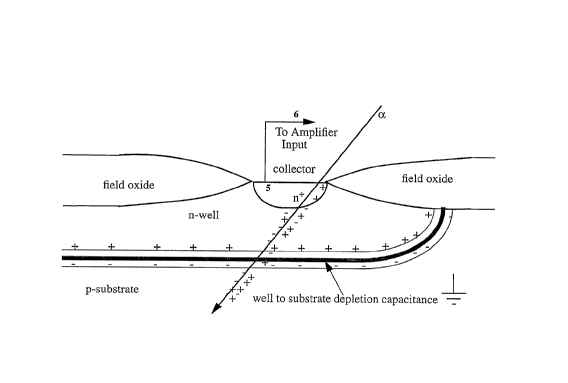
According to another aspect of the invention, a sense capacitor Cs 5 formed by the well
to substrate depletion capacitance of a reverse-biased well-to-substrate pn junction, shown
in Figure 2, is used to sense the alphas produced in the decay of radon. The sense capacitor
can be formed using either the n-well or p-well in standard CMOS processes. Collected
charge delivered by incident alpha particles on a sense capacitor formed in an n-well will
lower the potential across the junction by an amount ~Vin, whereas the converse is true for
a p-well capacitor. No preference exists in either choice. For the purpose of illustration a
sense capacitor formed in an n-well CMOS process is discussed here.
Figure 3 shows yet another aspect of the invention depicting the schematic of the
amplifier and its inventive application in radon detection. The amplifier is formed using a
CMOS digital inverter formed by two complementary devices, transistors MPl and MNI,
operated in saturation. The dimensions of both the transistors are ratioed to lower the
quiescent point as shown in the static transfer characteristic. The transistor dimensions are
further optimized to provide m~ximum gain with minimum input capacitance to avoid any
undue loss in ~Vin. The amplifier choice also provides maximum area coverage for C s
compared to that of the rem~ining circuitry, an important factor to achieve compact Iayout.
To prepare the cell in Figure 3 for operation as a detector, the n-well of Cs is connected
to the input 6 of the CMOS inverter amplifier, a high impedance point, which serves to
amplify the induced ~Vin. Operation begins by precharging the n-well to a positive
CA 02207337 1997-06-23
potential relative to the substrate. During the precharge cycle the PMOS transistor MP2 is
turned on by taking the gate voltage ~ 7 to 0 volts, the inverter is forced to the condition Vin
= VOut and the sense capacitor is precharged to the same potential. The dummy transistor
MP3 with its source and drain shorted to the signal line 6 is used to apply an opposing clock
feedthrough to that generated by MP2. To minimi7e the clock feedthrough of the circuit,
the size of transistor MP2 is chosen with twice the minimllm geometry (minimum transistor
dimensions allowed by the technology design rules) such that the corresponding channel
area of MP3 is half that of MP2. After precharge, a collection interval begins during which
the n-well is allowed to "float" electrically and Cs is expected to hold its charge until the
next precharge cycle. The collection cycle must be short enough such that Cs does not
discharge significantly due to junction leakage. The collection interval starts when MP2 is
turned off and MP3 turns on. Any alpha particle strike on the sense capacitor during this
collection time will cause a potential change at the input node and thus upset the Vin = VOut
condition. If the precharge point is chosen on the edge of the high gain region of the
inverter, as shown in Figure 3, the relatively small change, ~Vin, in Vin, produced by an
alpha strike, will lead to a large change, ~VOut, in VOut, which can be detected as a change
in logic level using an ~.~fiately designed buffer. The next precharge cycle will charge
the sense capacitor back to the Vin = VOut point if an alpha strike has occurred.
According to yet another aspect of the invention, transistor MP4 is used to lower the
power consumption. The need for lowering the consumption arises due to the fact that the
CA 02207337 1997-06-23
devices MPl and MNl are both operating under saturation and power is consumed during
both the precharge and collection cycles. Therefore, MP4 is turned on only during the read
and precharge cycles which are ~ 2% of the complete clock cycle. This scheme
significantly reduces power consumption to levels such that when an array of cells depicted
in Figure 4 is used in the design of single chip radon detector, the total average power can
be sustained by using a conventional alkaline battery source that would last for a few
months. In addition, the above scheme also significantly reduces the possibility of noise
coupling from power supply lines.
According to other aspects of the invention, the choice of this amplifier also allows the
design to be implemented in a p-well process by simply dimensioning the transistors MPI
and MNl such that the transfer characteristic is shifted towards VDD SO that a small
increase in Vin caused by an alpha strike produces a large swing at the output in an opposite
direction. The overall amplifier design provides high gain, low power consumption, low
noise, and maximum area coverage by Cs compared to that of the rem~inin~ circuitry. The
output from the amplifier buffered to a display reflects the count of alpha strikes from
which indoor radon concentration may be estimated accurately. This is yet another
improvement to the prior art detectors in that no additional complicated circuitry is
required to interpret the results.
The recommended guideline set by the EPA for indoor radon concentration is 4pCi/L
of air. At 4pCi/L of radon concentration, the expected count rate for alpha particles from
CA 02207337 1997-06-23
radon and its progeny in a volume of 20 cm3 reaching a detector surface is 20 counts per
hour. In an embodiment of this invention using the electrostatic collector 1, the sense
surface below the Mylar sheet 2 is made with an area of 1 cm2. The main constraint on the
maximum size of the sense capacitor is the fact that the charge generated by an alpha
strike must be comparable to that in the capacitor. Therefore, a well to substrate depletion
capacitance of ~0.4pF is considered to be a good choice. In another embodiment of this
invention, C~; is implemented in a square geometry of 100~m x 100,um in a conventional
CMOS process to give a value of 0.4pF. In order to obtain a sense area of lcm x lcm a
total of 10,000 cells are required. There~ore, an array of 10,000 inventive repeatable cell
illustrated in Figure 4, has to be placed in rows and columns in order to obtain an e~fecti~e
sense area of ~ lcm x lcm. Considering, 128 rows x 128 columns will require 16384
repeatable cells. Two 7-128 decoding blocks will be required to decode the rows and
columns, as shown in Figure 5. Similarly, two 7-bit counters 12 and 13 are required which
will divide the PRE signal 11 to be multiplexed by the row and column decoding blocks,
14 and 15. Outputs from the 7-bit counter 12 which is clocked using the PRE signal 11,
are fed into the row decoder block 14. The carry signal 16 of the counter 12 is used to
clock the 7-bit counter 13 whose outputs are fed into the column decoder block 15. This
scheme provides suitable multiplexing of the PRE signal 11 such that one column at a
time is accessed. The repetitive cells illustrated in Figure 4 will be butted together such
that each row will share same RSi signal line 10 and each column will share the same CSi
CA 02207337 1997-06-23
line 9. The outputs 17 of all the cells are wired ORed.
From another aspect of this invention, it was found that the maximum time after which
the sense capacitor discharges due to leakage giving a false output is 80msec. Therefore, if
PRE signal 11 of 411sec period is used all the 16384 cells will be accessed in 65.5 msec.
Half the period of PRE will be used for read (active-high) and the rem~inin~ half for
precharge (active-low). The RS 10 and CS 9 (both active-high) from the row and column
decoder outputs will be further decoded by the clock generating circuitry on each cell to
produce a ADDR 8 active-low signal that will select and power up the respective cell when
accessed. The output is valid only during the 2 ,usec when the ADDR signal 8 is low. The
clock generating circuity of a cell will also produce the ~ signal 7 to precharge the cell to
the Vin = Vout point-
The trapped radon gas after under going decay inside the collector of Figure 1 willproduce alpha emitting cl~llghter products that will be deposited on the Mylar sheet 3. Each
incident alpha particle will produce a change in the voltage only in the sense capacitor of
the cell at which it strikes. When the targeted capacitor is addressed it will have already
upset the Vin =VOUt point of the amplifier and a corresponding large output voltage change
is produced that is valid during the first 2~sec of the PRE pulse, the read cycle. In the next
2,usec of the PRE pulse, the capacitor is again precharged to Vin -VOUt. The output 18
carried through a properly designed buffer will provide direct count rate. This count rate
can be directly referred to the sensitive volume of 20 cm3 and a direct and accurate estimate
CA 02207337 1997-06-23
of indoor radon concentration can be made assuming equilibrium between radon and the
decay products.
In another embodiment of this invention, a single integrated circuit with 16 cells
arranged in 4 rows and 4 columns with the required on-chip clock generation and decoding
circuilly was designed and fabricated through the (~n~ n Microelectronics Corporation
(CMC) in 1.5 ,um CMOS process of MITEL Corporation, and later tested. A layout of this
embodiment is shown in Figure 6. The test results confirmed the functionality of the circuit
as expected.
The above embodiments of the invention also provide detector immllnity to change in
temperature and other process parameters since calibration is made to the Vin =VOut point
and not to an absolute value. The final size of the radon detecting chip is expected to be
approximately 1.5 cm x 1.5 cm with one clock supplied possibly by a crystal oscillator.
This simple, inexpensive and yet accurate radon detector is expected to be affordable for
continuous monitoring of indoor radon in the price range of present smoke detectors.