Note: Descriptions are shown in the official language in which they were submitted.
CA 02207350 1999-09-03
GAIN CONTROLLER
BACKGROUND OF THE INVENTION
1. Field of the invention
The present invention generally relates to gain control
of a variable-gain amplifier and, in particular, to a gain control
method and apparatus suitable for a system necessitating fine
gain control such as a DS-CDMA (Direct Sequence-Code Division
Multiple Access) system.
2. Description of the Related Art
In a DS-CDMA system, a plurality of channels are assigned
to a single frequency band, and each user's PN (pseudorandom
noise ) sequence is generated by a unique code to allow receivers
to distinguish among different user's signals. That is, the
receiver performs reverse-spreading or despreading of the
received signal by multiplying it by a replica of the PN sequence
used at the transmitter. Since the receiver uses a PN code unique
to the desired user signal, the signals coded with other users'
codes simply appear as noise, resulting in deteriorated quality
of communications .
Therefore, it is important that the power of each user's
transmitter is controlled by the central base station so that
CA 02207350 1999-09-03
2
the same power is received from every terminal and the power level
is constant with time. In other words, the transmission power
of each terminal must be precisely controlled in any DS-CDMA
system serving mobile users. According to Interim Standard 95
(IS 95) released by TIA (Telecommunications Industry
Association) in North America for Code Division Multiple Access
(CDMA), transmission power tolerance is specified at ~ 0.5dB.
Further, the receiver performs reverse-spreading of the received
signal to distinguish among different users' signals. Therefore,
fine gain control is also necessary for the receiver of each
terminal to perform linear signal processing.
The transmission power control and the gain control as
described above are performed by an automatic gain control (AGC)
circuit using a variable-gain amplifier. More specifically, the
output level of the variable-gain amplifier is compared with a
target level, and the gain of the variable-gain amplifier is
controlled so as to reduce the difference between the output level
and the target level according to the comparison result.
To achieve the precise AGC characteristic, the gain of the
variable-gain amplifier should be linearly changed according to
a gain control s ignal SD over a wide dynamic range . However , in
general, a variable-gain amplifier does not have the linear gain
control characteristic over its whole dynamic range but a
non-linear gain control characteristic as shown by a
characteristic curve 10 in Fig. lA. Therefore, it is necessary
CA 02207350 1999-09-03
3
to correct the gain control signal Sp applied to the variable-gain
amplifier so as to provide the linear gain control
characteristic.
According to a conventional AGC circuit , a correction table
is previously stored onto a memory such as ROM, and the gain
control signal Sp to be applied to the variable-gain amplifier
is corrected using the correction table. More specifically, as
shown in Fig. lA, a plurality of discrete points (in this figure,
gain values Gl-G9 and gain control values C1-C9) are previously
sampled from the characteristic curve 10 of the variable-gain
amplifier over the gain control range, and a set of discrete data
showing the relationship between the discrete gain values Gl-
G9 and gain control values C1-C9 of the gain control signal Sp is
stored in the memory. Such discrete data reduce the amount of
data stored in the memory. By the linear interpolation using
the discrete data of the correction table, the gain control signal
SD is corrected to provide the linear gain control characteristic
to the variable-gain amplifier.
Such a control method using a correction table as mentioned
above has been disclosed in Japanese Patent Laid-open No.
63-167557. Although the control circuit is included in a
semiconductor laser driver, the output power of the laser is
automatically controlled by a feedback loop using the correction
table.
However, the conventional control method and AGC circuit
CA 02207350 1999-09-03
4
cannot provide precise correction of the gain control signal Sp
to be applied to the variable-gain amplifier. As described above,
the gain control range of the variable-gain amplifier is equally
divided to obtain the discrete gain values Gl-G9 as shown in Fig.
lA. And the gain control values between the discrete values of
the gain control signal SD can be obtained by linear interpolation
from the correction table. Therefore, in cases where the
characteristic curve 10 has a sharp curvature, the corrected gain
control signal derives from an ideal gain control signal at the
location of that sharp curvature.
More specifically, when the characteristic curve 10 has
a sharp curvature ( for example , between the gain control values
Cl and CZ , C, and Ce , or CB and C9 in Fig . lA ) , as shown in Fig .
1B, a corrected output characteristic curve 11 of the
variable-gain amplifier deviates from an actual output
characteristic curve 12 between sample positions S1 and S2, S~
and Se, or Se and S9. Such a deviation causes the power control
in the DS-CDMA system to be deteriorated, resulting in reduced
quality of communication.
SUMMARY OF THE INVENTION
An object of the present invention is to provide a gain
control method and apparatus which can achieve precise gain
CA 02207350 1999-09-03
control of a variable-gain amplifier.
Another object of the present invention is to provide a
gain control method and apparatus which can provide precise power
control to achieve high quality of communication in a DS-CDMA
5 system.
According to the present invention, in a gain control
apparatus for controlling a gain of a variable-gain amplifier
based on an error signal corresponding to a difference between
an output level of the variable-gain amplifier and a reference
level, discrete characteristic data are sampled from a gain
control characteristic of the variable-gain amplifier in
sampling steps each being set depending on a variation of the
gain control characteristic. The discrete characteristic data
are stored in a memory. A correction controller corrects the
error signal based on continuous characteristic data generated
from the discrete characteristic data stored in the memory so
that the gain control characteristic of the variable-gain
amplifier is substantially linear with respect to the error
signal.
Since each sampling step is set depending on a variation
of the gain control characteristic, the continuous
characteristic data generated from the discrete characteristic
data is closely analogous to the gain control characteristic of
the variable-gain amplifier. Therefore, the error signal can
be precisely corrected so that the gain control characteristic
CA 02207350 1999-09-03
6
of the variable-gain amplifier is substantially linear with
respect to the error signal, resulting in precise gain control
of a variable-gain amplifier and improved quality of
communication in the DS-CDMA system.
BRIEF DESCRIPTION OF THE DRAWINGS
Fig. 1A is a diagram showing a gain control characteristic
curve of a variable-gain amplifier for explanation of a
conventional correction method for a gain control signal;
Fig. 1B is a diagram showing an output characteristic curve
of the variable-gain amplifier controlled according to the
conventional correction method;
Fig . 2 is a block diagram showing an automatic gain control
circuit according to an embodiment of the present invention;
Fig. 3 is a block diagram showing an example of a gain
control signal controller in the embodiment as shown .in Fig . 2 ;
Fig. 4A is a diagram showing a gain control characteristic
curve of a variable-gain amplifier for explanation of a
correction method for a gain control signal according to the
CA 02207350 1999-09-03
7
embodiment;
Fig. 4B is a diagram showing a gain control characteristic
curve of a variable-gain amplifier with respect to an accumulated
error signal for explanation of the correction method for a gain
control signal according to the embodiment;
Fig. 4C is a diagram showing an output characteristic curve
of the variable-gain amplifier controlled according to the
embodiment;
Fig. 5 is a block diagram showing another example of a gain
control signal controller in another embodiment of the present
invention; and
Fig . 6 is a block diagram showing receiver and transmitter
employing the embodiment of the present invention in a DS-CDMA
system.
DETAILED DESCRIPTION OF THE PREFERRED EMBODIMENTS
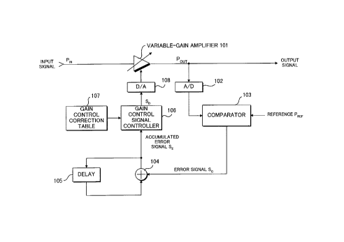
Referring to Fig. 2, there is shown an AGC circuit in
accordance with an embodiment of the present invention. The AGC
circuit controls the gain of a variable-gain amplifier 101 so
CA 02207350 1999-09-03
8
that the output level of an analog output signal POUT is kept at
a reference output level or target level PREF
The analog output signal POUT of the variable-gain amplifier
101 is converted to a digital signal by an analog-to-digital
converter 102, and the digital output signal is supplied to a
comparator 103. The comparator 103 compares the power level of
the output signal with the reference output level PREP to produce
an error signal S~ representing the difference between the output
level of the output signal POUT and the reference output level
lO PREF' For example, when the output level is greater than the
reference level PREF~ the error signal S~ rises to a positive value
corresponding to the difference therebetween. Contrarily, when
the output level is smaller than the reference level PREF~ the
error signal S~ falls to a negative value corresponding to the
difference therebetween . The error signal S~ is accumulated by
an accumulator or a filter to produce an accumulated error signal
SE. The accumulator is comprised of an adder 104 and a delay
section 105 which are connected such that the output of the adder
104 is delayed by the delay section 105 whose output is added
to the error signal S~ by the adder 104. The accumulated error
signal SE becomes larger when the error signal S~ is positive and
becomes smaller when the error signal S~ is negative.
The accumulated error signal SE is corrected by a gain
control signal controller 106 using a gain control correction
table 107 stored in a memory. As will be described in detail,
CA 02207350 1999-09-03
9
the gain control correction table 107 previously stores the gain
control characteristic of the variable-gain amplifier 101. By
using the gain control correction table 107, the gain control
signal controller 106 corrects the accumulated error signal SE
to produce a digital gain control signal so as to achieve the
linear AGC characteristic of the variable-gain amplifier 101.
The digital gain control signal generated by the gain control
signal controller 106 is converted to an analog gain control
signal SD by a digital-to-analog converter 108. The analog gain
control signal SD is applied to the control terminal of the
variable-gain amplifier 101.
Referring to Fig. 3, the gain control signal controller
106 is comprised of a correction controller 201 and an adder 202.
The correction controller 201 receives the accumulated error
signal SE from the adder 104 of the accumulator and produces a
correction signal 0 S by linear interpolation using the gain
control correction table 107 . The correction signal D S is added
to the accumulated error signal SE by the adder 202 to produce
the digital gain control signal. The contents of the gain control
correction table 107 and the operation of the correction
controller 201 will be described in detail referring to Figs.
4A to 4C.
Referring to Fig. 4A, the gain control correction table
107 previously stores a plurality of discrete points (in this
f figure , gain values G1-G9 and gain control values C1-C9 ) which are
CA 02207350 1999-09-03
v
sampled from the characteristic curve 10 of the variable-gain
amplifier 101 over the gain control range. More specifically,
discrete points are sampled at smaller steps as the curvature
of the characteristic curve 10 becomes sharper. In other words,
5 a sampling step is determined so that the linear interpolation
is sufficiently effective. As shown in Fig. 4A, since the
characteristic curve 10 is relatively sharp in a higher gain range
between gain control values C1 and C3, the corresponding discrete
points are sampled at smaller steps. In a middle gain range
10 between gain control values C3 and CS where the characteristic
curve 10 is almost linear, the corresponding discrete points are
sampled at larger steps. And, since the characteristic curve
10 is relatively sharp in a lower gain range between gain control
values CS and C9, the corresponding discrete points are sampled
at smaller steps . In this manner, a set of discrete data showing
the relationship between the discrete gain values and the gain
control values is stored in the gain control correction table
107 as shown in Fig. 3.
The correction controller 201 performs the linear
interpolation from the gain control correction table 107 to
produce continuing characteristic data which is used to produce
the correction signal O S so as to provide the linear gain control
characteristic with respect to the accumulated error signal SE.
More specifically, referring to Fig. 4B, the correction
controller 201 generates the correction signal O S using the gain
CA 02207350 1999-09-03
11
control correction table 107 so that the gain control
characteristic of the variable-gain amplifier 101 is
substantially linear with respect to the accumulated error signal
SE. According to the present invention, as described above, the
discrete characteristic data is sampled in sampling steps each
of which is determined depending on the degree of a curvature
of the gain control characteristic curve 10. Therefore, the
linear interpolation is more effective, resulting in improved
linear gain control characteristic of the AGC circuit.
Referring to Fig. 4C, as a result, even when the
characteristic curve 10 has a sharp curvature (for example,
between the gain control values C1 and CZ, C, and Ce, or Ce and
C9 in Fig. 4A), as shown in Fig. 4C, a corrected output
characteristic curve of the variable-gain amplifier is
substantially coincident with an actual output characteristic
curve over the whole range, especially between sample positions
S1 and S2, S~ and Se, or S8 and S9. Such an advantage causes the
power control in the DS-CDMA system to be improved, resulting
in improved quality of communication.
Referring to Fig. 5, the AGC circuit may be formed with
analog signal processing. In this case, the gain control signal
controller 106 receives an analog accumulated error signal SE from
the accumulator. The gain control signal controller 106 is
comprised of the correction controller 201, an analog-to-digital
converter 301, a digital-to-analog converter 302 and an analog
CA 02207350 1999-09-03
12
adder 303. The analog accumulated error signal SE is converted
to a digital form and is output to the correction controller 201.
The correction data generated by the correction controller 201
is converted to an analog form and the analog correction signal
D S is added to the analog accumulated error signal SE to produce
the gain control signal Sp.
In radio communications of the DS-CDMA system, there are
cases where the transmission power level is determined depending
on the received signal level. More specifically, when the
received signal level is relatively high, there is a strong
likelihood of the mobile terminal being located near a radio base
station. Therefore, in this case, the transmission power is set
to a reduced level. Contrarily, when the received signal level
is relatively low, the transmission power is set to an increased
level. Such a transceiver of the mobile terminal transceiver
in the DS-CDMA mobile communications system will be described
hereinaf ter .
Referring to Fig . 6 , a receiver of the transceiver employs
the digital or analog AGC circuit as shown in Fig . 1 or Fig . 5 .
The output level of the output signal Pot,.r~R~ of the variable-gain
amplifier 401 is compared with the reference output level PREFcR~
by a comparator 402 which produces an error signal S~~R~ . The error
signal S~~R~ is accumulated by an accumulator 403 to produce an
accumulated error signal SE~R~ . The accumulated error signal SE~R~
is corrected by a gain control signal controller 404 using a gain
CA 02207350 1999-09-03
.-
13
control correction table 405 as described before. The gain
control signal controller 404 corrects the accumulated error
signal SE~R~ to produce a gain control signal Sp~R~ so as to achieve
the linear AGC characteristic of the variable-gain amplifier 401.
Similarly, a transmitter of the transceiver also employs
the digital or analog AGC circuit as shown in Fig . 1 or Fig . 5 .
The output level of the output signal Po"TcT~ of the variable-gain
amplifier 501 is compared with a reference output level PREFcT> bY
a comparator 502 which produces an error signal S~~T~ . The error
signal S~~T~ is accumulated by an accumulator 503 to produce an
accumulated error signal SE~T~ . The accumulated error signal SE~T~
is corrected by a gain control signal controller 504 using a gain
control correction table 505 as described before. The gain
control signal controller 504 corrects the accumulated error
signal SE~T~ to produce a gain control signal Sp~T~ so as to achieve
the linear AGC characteristic of the variable-gain amplifier 501.
In the transmitter, the comparator 502 receives the
reference output level PREFcT> from a RX/TX gain converter
controller 506. The accumulated error signal SE~R~ generated by
the accumulator 403 of the receiver is converted to the reference
output level PREFcT~ for the transmitter by the RX/TX gain converter
controller 506. Therefore, the transmission power level is
determined depending on the received signal level.
Since the transceiver employs an AGC circuit according to
the present invention, the precise power control is achieved,
CA 02207350 1999-09-03
14
resulting in improved quality of communication in the DS-CDMA
system.