Note: Descriptions are shown in the official language in which they were submitted.
CA 02207488 1997-06-11
W O96118892 PCTAUS9S/IS9SI
- 1 -
AUTOMATED ELECTROPHORESIS AND FLUORlESCENCE
DETECT~ON APPARATUS AND METHOD
DESCRIPTION
I. BACKGROUND OF THE INVENTION
This application relates to a method and apparatus for rapid gel electrophoresis and
fluorescence detection of a complex m.,~Lule of fluorophore labeled proteins or nucleic acids.
Polyacrylarnide gel electrophoresis (PAGE) separation of organic molecules is now
S routinely performed. Current Protocols in Molecular Biology, Chap. 10, John Wiley & Sons
(1994). A polyacrylamide gel provides a suitably insoluble sieve so as to permit the separation
of organic molecules in solution by size and confo~ alion as they are drawn through the sieve
under electromotive force. guch separation of organic molecules provides valuable in~ight~
into their structures and functions. For example, PAGE separation can separate two
10 polypeptides of the same size but of dirre-tl-t isoforms or polypeptides only 100 daltons
dirrerellL in size (Current Protocols, 1994). Anot_er use for PAGE is in separation of nucleic
acids based on size of fr~gment~, such as in the extremely important application of DNA
sequence ~let~rmin~tion. ~ni~ti~, Molecular Cloning, A LaboratoryManual, 2nd ed., 1987.
Early methods for detection of separated products on an electrophoresis gel were15 carried out after the separation was completed. To the extent these techniques were
~-tom~ted in an apparatus, the apparatus generally inclu~iing a mech~ni~m for moving the gel
in stages relative to a detector. For example, US Patent No. 4,343,991 discloses a sample
detection apparatus in which stained bands within a gel are detected by transporting the gel
b~lweell an array of optical fibers supplying incident light and an array of optical fibers
20 collecting tr~n~mhted light. Information was collected in steps along the whole length of the
gel. Devices of this type have the advantage that long sample collection times can be used
when necess~ry to ensure detection of low intensity bands in the gel. However, they also have
several drawbacks. In particular, because the gel is analyzed only after separation is
completed, the degree of separation is necess~rily a co~ lo.,lise between the desire to observe
~ CA 02207488 1997-06-11
t'ast mi(~ratin~ bands (~llich run off the end of tlle gel if the electrophoresis proceeds toolc)n(~)
and the desire to separate slow movin~ band (which are still ~Jrouped to~ether if the
electroplloresis run is too short) In addition, the use of disthlct separation and detection
processes sigllifical1tly lengthel1ed the thne required to complete an analysis. Thus~ the art has
gellerally soug~ht the ability to detect bands on an electrophoresis ~gel during the ~eparatiol1
Wl1en the electrophoresed molecules are labeled with a detectable si~nal~ itis possible
to detect the separations of molecules in real time. Since the first description of a real-thne
nucleic acid separation method and apparatus by Smith et al., Sequence Detection in
Automated DNA Sequence Analysis", Nclt~ 321: 674-679 ( 1986), the technology for
10 so-called automated DNA sequencing has expanded rapidly. Several automated DNA
sequencin,~ apparatuses are commercially available. Methods and apparatus for sequencin~ of
DNA are described in U.S. Patents Nos. 4,8 11 ,2 1 8, ~,88 1,8 1 "; 5,06'',94~; 5,09 1 ,65;
~, I 0~ 1 79; ~ ,345: 5,16~,654; 5,1 7 1 ,534; ~,190,63''; 5,'07,880; 5,~ 13,673; 5,'~30,781,
~,~4 ~,~67, 5,~90,419; 5,~94,3 3; ~,307,148; 5,3 14,60'', 5,3~4,401; and 5,360,5~3 which are
1~ hlcorporated herein by reference.
Unfortunately, the e.Yisting apparatuses are inadequate for use of PAGE for emergino
clinical dia2nostic purposes such as dia~nostic DNA sequence and fragment analysis. For
clinical diagnostic DNA analysis~ it is desirable to examine hundreds of complex DNA samples
per day Existing technology does not provide for such capacity. For e:cample, operation of a
~0 typical automated DNA sequencer to ev~luate ~t most about 10 samples requires that a skilled
techllician spend up to four hours constructing a ,~el holder, filling the gel holder with actively
polyn-erizin~ acrylamide solution, inserting a well-formin~ comb before substantial
polvll1eri2ation has occurred, and waitin(~ for the oel to polymerize (see Maniatis, 1987).
IJS;I1~ tlle gel is equally time consumill~. Existing technolo(Jies use low density electric fields
'~ (less than 100 volts/cm) requiring sample running times of up to four hours. It would be
advantageous to have an improved apparatus with improved sample throughput for real-time
DNA analysis particularly for use in clinical diagnostic applications.
International Patent Publication No. WO 94/03631 discloses an assay method for
detection of analytes through the formation and detection of specific-binding complexes. The
. 0 complexes are detected after electrophoretic separation using an hlstrument in which a mirror
is used to successively illuminate individual detection locations on the gel. Emitted or
A~E~!~E~ S5~t~
IP~ ~P
CA 02207488 1997-06-11
WO 96/h8892 PCTlUS9S/lS9Sl
- 3 -
It is a further object ofthe invention to provide improved optical excitation and
detection techniques for real time detection of fluorescently labeled DNA or protein samIlles in
an electrophoresis gel.
S II. SUMMARY OF THE INVErNTION
The present invention achieves these and other objects by providing improved
~letech-)n methods and a~al~lus which may be used individually or in various combinations to
çnh~nce the ability of the electrophoresis apparatus to detect fluorophore- labeled m~ten~l~ in
short periods of time. Thus, one embodiment of the present invention is an apparatus for
10 electrophoretic separation and real-time detection of a sample labeled with a fluorophore
c mpri.cing
(a) a housing adapted to receive an electrophoresis gel holder;
(b) an excitation source of elec~lu.llagnetic radiation;
(c) means for sequentially delivering ele~ wllagnetic radiation from the excitation
15 source to each of a plurality of pre-defined excitation/detection sites within a linear array of
excitation/detection sites on a gel holder disposed within the housing;
(d) means for applying an electric field for to a gel holder disposed within thehousing for separation of a sample applied to a gel within the holder; and
(e) means for detecting emissions from the sample at the excitation/detection site,
20 wherein the housing holds the gel holder in a fixed position relative to the means for
sequentially delivering electromagnetic radiation and the means for detecting emissions when
the gel holder is disposed within the housing.
The electrom~gnetic radiation can be delivered to the excitation/detection sites using a
plurality optical fibers or a spot array generation grating. In addition, the apparatus may
25 advantageously include optical ~wiLchi~g means for sequentially directing electrc)m~gnetic
radiation into one of several pre-defined groups, each group including two or more of the
excitation/detection sites, and means for correlating a detected emission with the ~wi~chillg of
the excitation electrom~gnetic radiation such th.~t a given emission may be linked with the
excitation/ detection site being irr~ ted For example, when optical fibers are used to deliver
30 the excitation electr m~gnetic radiation, the optical ~wi~cl~i~g means may alternate between
CA 02207488 1997-06-11
W O96118892 PCTrUS9S/lS9Sl
-4-
directing radiation from the source into every other optical fiber, or may provide radiation in
rotation to every third or fourth fiber.
A ~Itern~tive embodiment of the invention is an apparatus CO~ )liSillg
(a) a housing adapted to receive an electrophoresis gel holder;
(b) at least one light emitting diode disposed to deliver excitation energy of afrequency suitable for excitation of the fluorophore to an array of excitation/detection sites on
the gel holder, and
(c) a detector, for example a photodiode, for ~etecting emissions from the array of
excitation/detection sites. This latter form of the a~pa~ s is particularly advantageous due to
the low costs of light emitting diodes (LEDs) compared to coherent light sources (e.g. Iasers).
m. BRIEF DESCRIPTION OF THE DRAWINGS
Fig. 1 shows a sectional side view of an apparatus according to the invention;
Fig. 2 shows a mounting plate for use in the present invention;
Figs. 3A and 3B shows excitation and detection systems useful in the present
invention,
Fig. 4 shows a spot array generating grating system useful in the present invention;
Fig. 5 shows an excitation and detection system employed in one embodiment of the
present invention;
Fig. 6 shows a detection system useful in the present invention;
Figs. 7A and 7B show an ~It~ tive detection system useful in the present invention;
Fig. 8 shows a squashed excitation beamlet obtained using a cylindrical lens;
~ Figs. 9A, 9B and 9C show a further embodiment of the invention;
Fig. 10 shows an apertured barrier useful in the apparatus ofthe invention;
Fig. 11 shows a pler~ d A/D converter circuit; and
Figs. 12A-12E shows the output of a photomultiplier tube when sequencing ~I13 using
an apparatus of the invention.
CA 02207488 1997-06-11
W O96118892 P ~ AUS9S/I59SI
IV. DETAILED DESCRIPTION OF THE INVENTION
This application ~i.ccloscs a method and app~us for rapid gel electrophoresis and
real-time fluorescçnce detection of a complex ~ lur~ of fluorophore-labeled organic
~ molCC~
S Figure 1 shows a sectional side view of an appa-~lus in accordance with the present
invention. The a~p~lus has a housing 10 within which the means for electrophoretic
sep~r~tion and detection of the sample are disposed. The housing 10 advantageously provides
a sealed, light tight enviro~le. .l in which the processing of the sample is conll~.cte~
Within the housing 10, a loaded electrophoresis gel 102 within a gel holder 101 is
10 positioned on a mounting plate 109 which holds the gel in a fixed position relative to the
rPm~inder of the apparatus, including the excitation/detection portions of the apl)aralus. The
loaded gel is advantageously held in place using suction through the mounting plate 109
generated using suction pump 110 and tubing 11 3, although other methods of holding the
loaded gel in place may be used without departing from the spirit and scope of the invention.
Opposing ends of the loaded gel 102 are placed in contact with two electrodes, such as
solution electrodes 104 and 105. These electrodes are connected to a power supply 114
which generates an electric field within the gel. This field causes the sample to migrate in the
gel from loading site 103 towards detection site 106.
An excitation source 107 which supplies electromagnetic radiation having a frequency
20 effective to excite the fluorophore used as a label is disposed within the housing 10 such that
radiation from the excitation source 107 strikes the gel holder 101 at the detection site 106
causing any fluorophore labeled molecules at the detection site to emit light. This light is
collected using optical system 115 and detected using detector 108. The analog output signal
from detector 108 may then be converted to a digital signal using an A-to-D converter 1 l 6,
25 and output for further proc~esing andlor display.
The apparatus of the invention may be used with any type of electrophoresis gel and
gel holder. Preferably, however, the apparatus is used with an ultrathin electrophoresis gel
having a thickne~s of 25-250 rnicrons of the type disclosed and cl~im~cl in commonly assigned
US Patent Application No. 08/332,577 which is incorporated herein by reference. Using such
30 gels, in which the çxcit~tlon/detection site is within about 12 cm of the loading site, it is
possible to sequence up to 300 nucleotides (nt) in under 20 minutes. This is accomplished
, j, "f~,,~,r~ j 1 / i~ iY~
~ CA 02207488 1997-06-11
throuol~ tlle use of field densities of 10()-~0() volt/cm whicl1 are madc possible by the ht1pro~ ed
heat dissipatiQn which can be obtained usin~ ultratl~ rels. In addition. the volta(re n1av be
varied throu(~hout any 4iven sample run in order to allo~/ maximum separation of sample.
To enhance the heat dissipation wl1ich is achieved as a result of the use of tl-in (~els. the
prese11t invel1tiol1 preferably mai;es use of a vacuum mountin~ technique. In this techniclue. as
sh< Wl1 in Fi(rure 1, the (~el holder l O I is mounted 011 a thermally conductive ceramic plate.
109, preferablv made of alumina. Figure ~ shows tlle structure of the mountil1(r plate in more
detail. As shown, the plate has an openin~ I 6 cut to ali~n with the detection site 106. This
openh1~J is preferably beveled so that it is wider Otl the side away from the (Jel mountil1(~
10 surface 1 1''. The ~el mountin(J surface I I ' has canal I I I formed h1 it which is conl1ected to
vacuum pump 110 via ports 1''7 which are connected to tubin~ 113. The canal 1 l l is suitably
about 0.~4 cm [. I inches] wide (e.~. 0.'~34 cm L 09 inches]) and 1~7 cm [.05 h1cl1es] (e.~,
O. 1 19 cm [ 047 inches]) deep, and is sealed over by the back substrate of the ~el holder, l O I,
when properly mounted. The ti;,ht ju~taposition of the baci~ substrate with the ceramic plate
1~ ~,ives improved heat transference when compared to ed(Je clampin(J devices. Vacuum sealh1(J
also allows for e~quisite precision in focussin~, excitation sources~ as described below.
A heat sini; (not shown) consistin~ of an alumh1un1 or other heat conductil1~l metal
sheet with extended fins may be contacted with the baci; face of the ceramic plate in order to
ht1prove heat conductal1ce away from the ~el.
~o The planar electrophoresis ~el 10~ ~enerally contains a pluralitv of lanes for loadin(J
and detectin(J sample across the widtl- of the ,~el. In many prior art devices, for example the
device disclosed in US Patent No. 4,81 1,'~18, detection of various lanes is accompiished USil1(J
a sin~,le detector which moves across the width of the ~,el and collects data from each lane in
series. Because of the rapid pro~ress of sample throu~h the ~,el whicl- is achieved usin~, the
present invention, (under 300 v/cm electric field, there is only about six seconds betwee
oli,,onucleotides differin(r by one nucleotide), however, svstems ~~hicl1 require physical
n1ovement of a detector are inadequate to collect the data for each of the lanes Improvel11ents
h1 the delivery of excitation ener(Jy and the detection of emitted energJy therefore had to be
made as part of the development of an effective apparatus and method for hi~Jh throu~hput
3 0 electrophoretic separations.
I)elivery of E.Ycit71tion Ener~y
j~,._,,~,_p
CA 02207488 1997-06-11
W O96118892 PCTrUS9S/lS9SI
In one embodiment of the invention, illustrated in Figure 3A, excitation energy is
conveyed to the excitation site by a fixed mulffplexed fiber optic array, 20 l . Radiation, 202,
from a source such as a laser, or light emit~in~ diode, 203, is coupled, using a fiber launch or
the like, 204, into an optical fiber 205. Suitable optical fibers for this purpose are fibers of 125
S microns thi~kness with a core of 50 microns (if mlllhmo~e) or preferably a core of 3.7 microns
(single mode). The optical fiber carries the beam to a mini~ re board mollntable switch, 206,
that permits the ~wiLchi~g of an opffcal signal ~om one output fiber 210 to another. For
example, optical ~wilc~ g can be accomplished using a switch available from AMP, Inc.,
~ isburg, PA, in which a slight pivoting motion of a spherical mirror reflects the optical
10 signal into one oftwo output fibers. The switch takes ap~lvxi..~ ly 5-l0 milli~econds to
settle after each change. Several switches can be used in combination permitting the excitation
beam to be divided into any m3mber of output optical fibers 210.
As shown in Figure 3A, four output fibers 210 are used to permit the sequential
excitaffon of four groups of excitation/ detection sites. The use of four output fibers is merely
15 exemplary, however. In general, the allpalaLus of the invention will divide the incid~nt light
into from 2 to l0 groups.
Light in each output fiber 2 l 0 is con~lucted by the output optical fiber 2 l 0 to a beam
splitter 207A, 207B, 207C or 207D which separates the beam into a plurality of final optical
fibers 208, each conducting its respective fraction of the input excitation beam as an excitation
20 beamlet. Each of the split optical fibers conveys the beamlet to a SELFOC~ rod gradient
index (GR~N) lens 209 (NSG America, lnc.; Somerset NJ) which is fixed in location and
disposed to irradiate its respective excitation site, 106, one lens for each excitation site.
Exp~rim~nt~l evidence shows that use of the vacuum seal to mount the gel holder also
provides the advantage that the focal length of the GRIN lens can be exquisitely positioned
25 with respect to the ultra-thin gel. The vacuum seal holds the gel extremely flat against the
ceramic plate without the slight bowing or bending of gel holders found in edge clamped
apparatuses.
The final optical fi~ers 208 and the lenses 209 are disposed to form a linear array of
detection sites. Within this array, the final optical fibers 208 are ordered so that, when using
30 four groups of excitation signals, every fourth detection belongs to the same group. The
effect is that only a sub-set of excitation sites are irra~ ted at any one time (A, B, C, or D).
~ CA 02207488 1997-06-11
Of course, if one ~-~ere using two groups of excitation si~nals (only a single split of the incident
bean1 ~0'), the final optical fibers 708 would be arranged in an alternatingJ patten1 (see Fig.
3B). This provides the advantaae that a sin~le detector, 21 1, may be employed to detect
emissio11s from a plurality of excitation/ detection sites if the detector output is synchronized
5 with the switch so as to allow the si~o,nal processor to identify which signal came from which
excitation/detection site.
The optical switch, ~06, is programmed to switch the input laser beam into each of the
output fibers 210 (and thus into the final optical fibers '08), for a period of preferably 20-100
milliseconds. Synchronization of the switch and detectors may be obtained with a10 microprocessor, ~12.
The fixed multiplexed fiber optic array permits a high number of data points per second
to be taken from each lane of the gel by conveying pulsed irradiation to each excitation site.
Further, it permits use of a reduced number of detectors.
The fixed multiplexed fiber optic array can also be modified to brino dif~erent irradi-
15 ation sources to the same excitation site in a series of alternating pulses as shown in Fig. 3B.Such an arrangement is constructed by employing different excitation sources '03 and ~03',
each coupled to an optical fiber 205 and ''05'. An optical switch "20, operatina in the oppo-
site direction to switch 06 is employed to alternately select which source is to be conducted
to the optical switch 206 via optical fiber '21. This arrangement permits multicolor fiuores-
~0 cence imaging for use when more than one fluorophore is used in any given lane of the gel.
In a second embodiment of the invention, illustrated in Fiaure 4, radiation 301 from anexcitation source 107 is directed to the excitation site 106 by use of a multiple beam split
ter
30~, such as a Spot Array Generation Grating which splits the incident beam into a number of
beamiets, generally from 2 to 24 beamlets. Preferred diffraction gratin;,s are of the type
~5 i;nown as "transmissive" or "phase" gratings, because such gratings can be designed to
produce an even intensity distribution of light among the resulting beamlets. In the illustrated
embodiment, an incident laser beam of a frequency suitable for excitation of the fluorophore is
directed into a binary phase grating, approximately I cm square, mounted on glass, thermo-
plastic or the like of approximately .318 cm [1/8th inch] thickness (Semiconductor Technol-
30 ogy Inc, Pointe Claire, Quebec). The transmitted beam is divided into a linear array of thedesired
A~E~ . T --~
~ ~ _ f_ ~
CA 02207488 1997-06-11
W Og6/18892 PCTnUS9~1S9S
r of ~,~xci~tion beamlets, 303, one for each intended excitation site, 106. The beam~ets
are directed to a foc~ in~ lens, 304 (e.g., Stock # G69, 129, Catalog 1994, F~lmlln~i
~çjPntific) The focl~sing lens has in the embodiment shown preferably has a focal distance, f,
of 50S rn~L The spot at each excitation site can be varied in size by rh~n~n~ the distance, d,
5 between the lens and the excitation site. The spots are suitably beLween 0. lmm and 0.2 mm
m~ter In a ~,~;r~il.ed embodiment the spot array generation grating divides the incident
laser beam into a linear array of 16 spots, and the lens is disposed between 200 to 500 mm
from the gel.
As will be apparent to those skilled in the art, any excitation source can be used in
10 embo~ utili7ing a fiber optic array or a spot array generating grating, provided that the
source is matched with the fluorophore to be used so that the radiation from the source excites
the fluorophore to stimlll~te emission of cletect~ble r~ ti-)n For example, the following
non-limiting examples of c~ r~;ially available excitation sources can be e-m--ployed in the
present invention: Optical lasers, e.g., Argon ion lasers, Argon hypton mixed gas lasers,
15 ~eli~lm-neon lasers and doubled YAG lasers; Laser Diodes, Fiber (Solid State) Lasers; and
Blue, Green, Red or infra red-Light Emitting Diodes (LEDs).
In a third embodiment of the invention, illustrated in Figure 5, an independent
excitation source is used for each excitation site. An effective and extremely low cost
excitation source for this purpose is a light emitting diode for example those available from
20 Stanley Corp. and identified as Type No. AN, BN, CN or DN. Unlike lasers, LEDs emit light
in a broad band spectrurIL Bandpass filters 403 disposed between the excitation/ detection site
106 and the detector 402 should therefore be carefully selected to elimin~te as much
overlapping excitation irradiation from the detector as possible. One LED, 401, is disposed to
irradiate each excitation site, 106, with or without a focussing lens 404 to focus the emitted
2~ ~adiation. An LED can emit 1.5-1 SmW, sufficient to excite a population of fluorophores. In
this embodiment, using an infra-red L~D with Cy8 or Cy9 as a fluorophore, where the emitted
light is in the infra-red region, the detectQr is preferably a photodiode detector 402.
While it is possible to have each LED 401 in the array constantly illllmin~ted such that
data collection from each lane can be continllous, it may be advantageous to use a pulsed
30 excitation source in this embodiment as well. For example, where the lanes are close together,
CA 02207488 1997-06-11
Wo 96/18892 Pcrlusssllsssl
- 10-
pulsing ~It~rn~te lanes, or every fourth lane, may improve the accuracy of the detector by
çlimin~hn~ carry over form one lane to the next.
Fluorophores useful in the present invention are those which can be coupled to organic
molecules, particularly proteins and nucleic acids and which emit a detect~kle amount of
S electrom~gnetic radiation in response to excitation by an available excitation source. As used
herein, the term fluorophore encomra~ses materials having both fluorescent and phosphor-
escent emissions. It is desirable that the fluorophore exhibit a sufflcient Stokes shift to permit
filterin~ of emitted radiation from the excitation irr~ ti- n. A further limitin~ factor on the
choice of fluorophore is whether the fluorophore contains functional groups that prevent it
from surviving intact during the cleavage and deprotection reactions of commercially available
oligonucleotide synthesis.
Suitable fluorophores for this invention .nclude fluorescein and its analogs, rhodamine
and its analogs, cyanine and related polymethines and their analogs, and the like. Specific
fluorophores which are suitable for use with the present invention are Fluorescein
isothiocyanate (FlTC); 4-fluoro-7-nitrobenzofurazan (NBD-F); Texas Red~) (Molecular
Probes, Inc.; Eugene, OR); teLI~llelllyl rhodarnine isothiocyanate (TRITC); and Cyanine dyes,
especially, Cy5, Cy 5.5 Cy7, Cy7.5, Cy8 and Cy9 (Biological Detection Systems, Piu~bul~,
PA). Fluorescein fluorophores are preferably excited using an argon ion laser, while
rhodamine fluorophores are preferably excited using a helium neon laser. The cyanine dyes,
which are described in US Patents Nos. 4,981,977 and 5,268,486, which are incorporated
herein by reference, are useful in combination with a red or infrared LED excitation source
because the cyanine fluorophores Cy5 to Cy9 absorb and emit in the red and infra-red regions
or laser diodes. Infra-red emissions are detected preferably with photodiodes, and particularly
silicon photodiodes, 402, rather than PMTs.
An alt~m~tive to using LEDs in the above embodiment is use of laser diodes. Red and
infra-red laser diodes can be used to excite fluorophores such as Cy5, Cy5.5, and Cy7.
I:~ete~tion Qf FluorQPhore E~itted R~ ti~ n
Emissions from the fluorophores are detected by a detector disposed to receive
radiation from the detection site.
Figure 6 illustrates a first embodiment, particularly suited for use with a fixed
multiplexed fiber optic array. A linear array of detectors 501, is disposed to receive emissions
CA 02207488 1997-06-11
WO 96118892 PCTAUS9S/lS951
- 11 -
502, from a linear array of detection sites 106. A llet~ctor may be any two dimPn~ional
detector, such as a CCD, a photodiode or, in the ~l~r~ d embo~lim~.nt, a photom-lltiI-lier tube
(P~). Disposed between the detection site a~d the PMT are a collecting lens 503, a
bandpa~s filter 504, a foc~ ing lens 505, and a spatial filter 506. The b~ntlp~ filter is an
5 illlel~,c;ce filter (Omega Optical, Inc. Brattleboro, VT) or the like of 20 to 40 nm
tran~mission wavelength width chosen to transmit the fluoresc~n~e emission and to block
reflected light of the excitation source. The spatial filter is chosen to o~Lillf;~e recognition of
the band of fluorophore-labeled sample as it passes through the detection site. F.limin~tion of
fringes and tails of bands using a spatial filter tends to increase the signal to noise ratio of the
~etecte~ signal. P~r~lled spatial filters are rectan~ular in shape with a height of 100 microns
and width of 250 microns.
The detector collects a signal, which is integrated over a finite time-span and converted
to a digital output. A suitable integr~tion time for the invention is 5-100 milli~econds. When a
PMT is used to record a plurality of excitation/ detection sites, the width of the PMT is
selected in a manner con~i~tPnt with the number of sites. In general. PMT's with width of
from 3-15 mm, and preferably about 5 mm are suitable. In this case, the integration of signal
must be synchronized with the mllltiple~ing switch of the excitation irradiation source. Such
syncllr~ aLion can be controlled by a microprocessor 212. As stated above, a suitable period
of multiplex switching is 20-100 milli~econds, although any period that results in a sufflcient
number of data points for analysis can be used. Fluorescence emissions can therefore be
correlated with the respective detection site on the gel. Fluorophore must be chosen such that
the delay in fluor~scençe emission from an old detection site does not cause significant overlap
with the new fluor~cPnce emissions from a new detection site.
In another embodiment, if multiplexed excitation beams are not used, then a single
detector is required for each detection site. Any type of ~letector may be employed, such as
CCDs, PMTs or silicon photodiodes (Series S2386 or S2387; ~m~m~t~ll Photonics KK,
City, Japan). The silicon photodiode 601 is disposed at the focal distance of the
lens of the diode 603 from the a~arel.~ detection site 106 and to collect emitted light 602 in a
position out of ~lignm~nt with the excitation beam as illll~tr~tecl in Figures 7A and 7B.
ID Fig. 7A, the light 107 from the irradiation source is directed to the excitation site
along the huli~o~ l axis of the gel. A linear array of detectcrs can be positioned both above
' CA 02207488 1997-06-11
and belo-v said axis in diode holders ~0~. Thus, if a first linear array of detcctors is t'ocussed
at e~;citation sit s sta~ ered t;om the e.~citation sites recorded by tlle second 1inear arra~ of
detectors, it is possible to utilize twic~ as many excitation spots per gel. Further, a lhlear array
of detectors may be disposed on the opposite side of the (Jel. a ,ain above or belo~ the
5 horizontal axis of the gel. If all detectors detect excitation sites sta~ ered from each other, it
is possible to detect at least four excitation sites for every unit of detector width.
Fi~,. 7B shows an alternative embodiment of a photodiode detector usefill hl theinvention. Light 107 from the excitation source impin~es on the gel holder 101 at an an~le
relative to the surface of the ,~el holder. The detector element 70 collects light whicll is
10 emitted substantially perpendicular to the surface of the ~el holder 101 . The detector element
70 has a body member 701 in which a AR-coated (antirefiective) aspherical lens 71 1, two AR-
coated cut-offfilters 71 and 713 selected to transmit li~Jht ofthe emitted wavelen~tll, a
second AR-coated aspherical lens 71~ and a photodiode 715 are mounted. A spacin~ between
the filters (~ 1/'~ to 3/4 inch) may be used to reduce back~round radiation reaching the
1~ photodiode 71 ~, since radiation which is not directed straight into the detector is absorbed by
the interior of the body member 701.
All si~nals received from detectors are preferably converted from analo~r to di~gital and
conveyed to a serial port for transmission to a multipurpose computer for stora~e and for
further processin~ and analysis. It will be understood, however, that the analo;, output could
~0 be sent directlv to an output device for display or printing
ln selectingJ a combination of optics for use in the apparatus of the present invention, it
may be advantageous to use a lens to concentrate the excitation beam into a smaller area
withill the detection zone. In particular, it may be desirable to use a cylindrical lens which
reduces the dimension ofthe excitation beam in one direction (e.g. vertical) while leavin~ it
unaltered in the other (horizontal) direction. (Fi~. 8) Such a "squashed" e:;citation beam can
increase the resolution of the apparatus since a shorter length of the electrophoresis oel is
interro~ated.
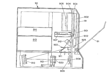
Fi~. 9A shows a cross-section view of a preferred embodiment of the present
invention. The various components of the apparatus are disposed within a housin~, 90, wllicl
'0 has a access door 91 the front thereof. The access door 91 is hinged to permit movement
between a closed position (solid line) and an open position (dashed line).
AM~ c~_~r~
~P~..Q~_P
CA 022074X8 l997-06-ll
W 096/18892 I~~ 9sll595
Within the housing 90, the gel holder 901 is held in position b~we~ two solutionelectrodes 902, 902' against mounting plate 903. The mounting plate 903 and the solution
electrodes pivot oulw~rd on pin 925 to facilitate loading of an electrophoresis gel. A heating
çl~mPnt 904 is disposed in thermal contact with the back surface of the l. .o~ ;..g plate 903 to
S permit heating of the gel. A fan 905 which is surrounded to a sub-housing 906 and vented to
the exterior of the housing 90 blows room temperature air across the back of the heating
e1em~nt 904. Through a combination of heating and cooli~g provided by the heating element
904 and fan 905, respectively, a desired temperature in the range of from 30 to 55 degrees C
can be m~in~ined to a tolerance of 0.5 degrees.
Figs. 9B and 9C show the mounting of the gel within the apparatus of Fig. 9A in
greater detail. Fig. 9B shows the electrode assembly when viewed from the inside. The
assembly is forrned from a base plate 930, a main body portion 931, and three reservoir wall
portions 932,933 and 934, all formed from plastic. The body portion 931 has a first reservoir
opening 935 cut in the top edge thereof and a second reservoir opening 936 cut in the bottom
edge thereof. Reservoir wall portion 934 entirely covers the outside face of reservoir opening
935 to partially define the upper solution electrode 902, while reservoir wall portion 932 at
least partially covers the outside face of reservoir opening 936.
Reservoir wall portion 933 is disposed on the interior surface of the of the body
portion 931. Reservoir wall portions 932 and 933, the base plate 930 and the body portio
931 together define the lower solution electrode 902'. Reservoir wall portion 933 has a
stepped region 937 within the lower solution electrode on which the edges of the gel holder
rest when in place. Wires 927, 927' extend across both solution electrodes 902, 902' to
provide the electric field for electrophoresis.
In use, as shown in Fig.9C, the gel holder 901 is placed on set portions 937 of the
reservoir wall member 933 so that the beveled edge is submerged within the upper solution
electrode 902 when it is filled with buffer. The electrode assembly is then tipped back into the
apparatus so that the gel holder 101 is sandwiched between the body member 931 and the
mounting plate 903, and held tightly in place using knurled knob screws. Gasket materials 926
disposed around the first reservoir opening 935 and on the interior surface of the body
member 931 act to seal the upper solution electrode 902 and to cushion the plessule on the
' CA 02207488 1997-06-11
gel holder 101 Buffer is added to the solution eiectrodes 902 and 90 ' and the sample is then
loaded onto the gel through the beveled opening.
A detector module 907 (Fig 9A) consisting of a linear array of photodiodes such as
those shown in Fig. 7B, each connected to a circuit board is aliOned with the e~ccitation
detection site in the gel, and collects light which is emitted perpendicular to the surface of the
~el holder 901. The circuit board contains an analog-to-digital (A/D) converter which
converts the analo~ current output of the diode to a digital volta~e si~nal. This di~ital signal
may then be further processed by the computer circuit board 914 disposed within the housing
or transmitted to an external computer for processing.
While essentially any conventional AJD converter can be employed in the apparatus of
the invention, preferred A/D converters are of the type described in US Patent Application
Serial No. 08/45'~,719 which is incorporated herein by reference. Briefly, in such a device as
shown in Fig. I 1, an eight-bit di~ital-to-analo(r converter (D/A) 1 103 is provided, which
~enerates an output on line 1 105. The output of the D/A is controlled by processor I 1 15
through di~ital bus 1 14. Digital bus 1 14 provides a select line and eight data lines 104 to the
D/A I 103. In this way, the processor I 1 15 can provide an offset or base level for the signal
beh1g processed.
The programmed offset from D/A 103 and the voltage level from amplifier I 10' are
summed and amplified by op amp 1 106. The output of op amp 1 106 is then provided to
0 hlte~rrator 1 107, which comprises an op amp, a highly stable capacitor 1 108, and related
components. Integrator 1 107 is controllable with respect to the starting and ending time of its
integration periods by analog switch I 109, controlled by discrete control line I I 10. The
output of the integrator 1 107 is provided to ,~VD I 1 12. AVD I 1 1~ is preferably a multiple-
illpUt ,LVD, and only one of its inputs is shown in Fig 1 I for clarity. AID 1 1 1 ' has a serial
control line 1 1~7 and a serial data line 1 1 13, which carries I ~ bits of data from the A/D
conversion process. Processor I 1 15 has a bidirectional serial link I 1 16 with a personal
computer or work station omitted for clarity in Fig. 11.
In an apparatus incorporating an ~VD circuit of this type, the dynamic range of the A/D
I I I '' is not spread out over the entire range of possible outputs from the detector I 100.
Instead, the offset from D/A 1 103 is used to set a base level which is the starting point for the
dynamic ran,~e of the iVD I 1 1~. In addition, the integratioll periods, namely periods durhlg
I p--,!~ ~--p
~ CA 02207488 1997-06-11
which switch 1 109 is open so that inte~ration takes place. are son-etimes sllort and sometimes
long. Shorteni_~ tlle integratioll period permits the A/D I I I ' to e~tract meanin(rt'ul data e~en
at times when the photon flu~; along path I 1 17 is very high, much hi~her than the flu:i durin~
times when a ta~ed nucleotide is present in the sensin(r area.
The excitation beam is provided by a laser diode 908 mounted in aligJnment witll an
aspherical lens 909. The asphericaî lens 909 collimates the output from the laser diode 908
and directs it towards a transmissive diffraction ,ratin~ 920 which divides the li;,ht from the
laser diode into 16 beamlets of substantially equal intensity. These beamlets are conducted by
lens 921 and mirrors 910, 91 I to a cylindrical lens 91~ which forms the squashed spots at the
excitation/detection sites. The mirrors 910, 91 I may be aluminum or aluminum coated (Jlass
when the excitation wavelength is below 650 nm, but are advantageously gold coated glass
when for loner wavelen ,ths because of the ;,reater reflectivity of ~old at these wavelen;,ths.
Dielectric mirrors may also be used although they are substantially more expensive.
Within the apparatus shown in Fig. 9, there is also an apertured barrier 9~ of the type
shown in Fi~. 10 between the last mirror 911 and the cylindrical lens 91~7 ali~rned so that each
beamlet passes through an individual hole ( 1-3 mm diameter) in the barrier. This barrier
reduces the amount of scattered li~ht WlliCIl reaches the excitation detection site.
A power supply 913is disposed within the housing 90 and is connected to the solution
electrodes 90~ to provide the volta~e gradient for electrophoresis.
~0 The sequencin~ apparatus of the invention can provide a signal directly to a dedicated
computer, for example a personal computer, for processin~ an sequence analysis. For many
applications~ however, improved performance at reduced cost can be obtahled by COllllCCtill~, a
number of sequencin~ apparatus to a sin~le computer hl a networl; confi~uration. For
example, several sequencers can be connected into a network as described in concurrently filed
''~ U.S. Patent Application No.081~70,994 whichis incorporated herein by reference. In this
case. the apparatus of the invention will also suitably include an on-board computer board 915
containing a buffer memory of sufficient size to store substantial portions of the data from a
sequencin~, run and a microprocessor for controllin2 the acquisition of data and the subsequent
transfer of this data to a shared network computer for sequence analysis processing.
Aî~ ) S~-~tc
IPI-~I~P
CA 02207488 1997-06-11
wo 96/18892 PCTIUS9511S9Sl
- 16-
It will be appreciated that the apparatus shown in Fig. 9 may incorporate additional
re~ s without in any way departing from the present invention. For example, a light may be
placed inside the housing which illllmin~tes the gel holder when the access door 91 is in the
open position to f~ilit~te loading of the appa~lus. Similarly, status lights and indicators may
S be disposed on the lower portion of the housing to indicate parameters such as the duration of
an on-going sequencing operation. The apparatus of Fig. 9 can also be used with an external
light source such as a laser and an optical train (for example fiber optics or mirrors) to direct
the light from the source to the aspherical lens 909.
10 Example
A single str~n~led M13 DNA molecule is hybridized to FITC labeled universal primer.
Sequencing reactions are undertaken using SEQUENASETM in the recommended reaction
buffers. After completion of r~ctio~c, loading buffer of xylene cyanol, bromophenol blue and
glycerol is added to the reaction tubes to provide a visible loading marker. A microgel,
lS~ d as disclosed in US Patent Application 08/332,577 is mounted on an ~ min~ plate by
vacuum seal. A solution electrode is affixed such that the upper chamber contacts the upper
end of the gel, and the lower ch~mher contacts the lower end of the gel. GRIN lenses, each
attached to its respective optical fiber of a fiber optic array are disposed at the focal length
from the excitation site near the lower end of the gel. An argon ion laser of 5 mW power
20 output, 488 nm wavelength is directed into the optical fiber by the fiber launch (upstream from
the beam splitter). A linear array of PMTs is disposed to receive fluorescence emissions from
the detection sites, one PMT per detection site. The M13 sample is loaded into the loading
site. An electric field of 250 v/cm is suspended across the gel. Electrophoresis of the sample
through the gel is recorded and displayed as in Figures 12A-12E, where the x-axis shows time
25in tenths of seconds. The data shows clearly resolved M13 sequence data out to 220 nt in 12
I--;llul~s