Note: Descriptions are shown in the official language in which they were submitted.
CA 02207705 1997-06-11
W O 96/21875 P~ 11540
MICROREPLICA~ED OPTICAL MODULE
Back~loulld ofthe Invention
1. Field of the Invention
The present invention genera11y relates to devices for op~ldlivt:ly
connecti~ the ends of waveguides such as optical fibers, and more palticularly to an
article which illlel-,o~ ects at least one optical fiber to at least one other optical fiber
and has a microrep1ic~te-1 planar structure with optical waveguides folmed therein.
2. Description of the Prior Art
0 With the wide commercialization of optical fiber nt:lw., ks, it has
become increasingly important to provide optical interconnection devic:es which are
not only easy to use and reliable, but which may further be m~nllf~ctllred inexpensively
in mass q ~ntities Optical splitters are of particular interest since they allow a single
(input) fiber to be interconnected with a plurality of (output) fibers, or allow optical
signals from multiple input fibers to be merged into a single waveguide. Splitters play
an important role in the use of optical fibers for teleco~ lul.lcations, cable television
and data tranemi~ n
Optical splitters are commonly made by fusing optical fibers, or by
p~ y att~rhing the fibers to a planar, glass inle~ ed optical de~rice which
guides the light from input fibers to output fibers (pigt~i1in~). Pi~ai1inlJ is a critical
step in the m~n11f~ctl1re of planar glass illle~;laled optical devices since the device cost
is proportionate to the number of fiber ~tt~c~ s desired. The pif~iling step
inr,1~1de~s both the ~lignment of the optical fiber w.1~uide paths with the ion-..iffllced
or channel waveguide paths in the splitter, and the ~tt~chm~nt of the fiber pigtail ends
at the colllponent end face. ~ nmPnt must be very precise, and the ~tt~hm~nt must
assure the stability ofthe ~lignmPnt during ellV-iO~ v~ri~tion.s Precise ~1ignm~nt
is often r~iffic~llt, especially for s.ingle-mode wavtiguides whose core ~ mP~tçrs are on
the order of 8 microns. This labor-intensive pi~i1ing process prohibits planar
integrated optical devices from being mass produced with econollly.
To reduce the cost of actively ~li nin~ optical fibers to an optical
waveguide device or coupler, it is known that the optical fibers may firs,t be il~St;l led
CA 02207705 1997-06-11
W O96/21875 PCTrUS95tl5406
into and pel"~A~ ly att~clled to a fiber ~ligning substrate which subsequently is
aligned and pe~ A~ ly ~tt~h~l to the optical waveguide substrate. Economy results
from the alignment of a plurality of optical fibers in one step. This method of fiber
q~tt~c~hment requires the pe~ enL ~tt~hm~nt ofthe fibers to the optical waveguide
5 device, and further requires polishing of the fiber ~ ninp substrate and optical
waveguide substrate prior to their ~tt~ m~nt to each other. See U.S. Patent No.
5,197,109.
A process for producing optical polymer col"ponents with an integrated
fiber-chip coupling mPçhAni~ is dic~losed in Patent Cooperation Treaty Application
lo No. WO 93/21550. This application teaches a process for fabricating integrated optic
co.,-pollents through the molding of polymeric materials. Fiber guiding grooves are
molded in precise registry with the integrated optical channel waveguides providing for
the passive ~lipnmçnt of optical fiber pigtails to the channel w~v~guide device. The
applic~tion further describes a process wherein the glass fiber ends are placed into
15 positioning grooves in the molded polymeric components and the Ope.~llgS are filled
with a poly."~ able monomer. With a cover plate applied, the m~teri~l is
polym~ri7~d in situ. The application fails to describe a method for quickly or reliably
splicing or connectinP~ a plurality of fibers to the microreplicated waveguide device,
nor does it teach any sort of housing ~nclosin~ or supporting the microreplicated
20 device.
A similar method for the production of optically h,le~ aLed w~ve~ ides
with fiber~ nce structures, and employing the molding of polymeric mz~t~ri~lc, is
depicted in U.S. Patent No. 5,311,604. That invention relates to the cimlllt~neous
production of optically integrated waveguides and micro-ll,e~ ic~l components for
25 fiber ~ nce An optical substrate contains at least one polymeric w~/eguide
structure, I,~,sre"ed in the form of ~ecesses by molding a polymeric ~ubsll~le. The
recesses are filled with a material having a higher refractive index than the substrate.
An optical substrate co~ at least one waveguide structure with at least one fiber-
n~e structure in polymers is also rlicrl~ sed Fiber ~ç~ is achieved by the
30 same ~ n.~... employed in WO 93/215~0, wLerehl the optical fiber ends are placed
into positioning grooves in the molded polymeric col"pone"Ls. A method is further
CA 0220770S 1997-06-11
W 096nl875 PC~nUS95/1S406
des~ilil,ed for the coupling of fibers to the optically integrated waveguide by inserting
the fibers into the fiber ~ nce recçcses; a cover plate is ~ d e~entling over the
fiber guiding recçccec The means for providing a low-loss, low back reflection
connection between the optical fibers and channel waveguides is not tallght, nor is any
~ 5 means taught for holding the optical fibers in precise fixed orient~tio~ vvith respect to
the channel wave~lidPc In another aspect ofthat invention, the fibers are inserted
into the ~ nce grooves and the openings are filled with a polyl-~k~ e mon-)m~r;
with a cover plate applied, the material is again polymerized in situ. The method of
ffber ~tt~--hmPnt is again p~llllatlelll and requires a clean room environment to
o Pl;,;; ~e the possibility of co~ ion ofthe waveguide ch~nnçlc during application
ofthe high refractive index poly.nel~able material. Field in.ct~ tion is thus quite
difficult if not impossible. The '604 also fails to teach a method for quieldy or reliably
splicing or c~nnectin~ a plurality of fibers to the microreplicated waveguide device in a
rern~te~ble fashion, nor does the application teach a housing enclosing or supporting
15 the device.
European Patent Applic~tion 560,043 discloses a method for producing
planar waveguide PlemPnts for optical fiber nt;lwolk~, and colnpol~.lls according to
this method. The ~pplic~tion claims a method for the production of passive, integrated
optic cG,."~)onel,Ls from polymeric m~tPri~lc, col~.ci~ p at least of a molded part with
20 ch~nn~lc for the optical waveguides and fiber-guidance grooves, and at ]east one
coupled fiber-like optical waveguide. The optical fibers may be coupled to the
integrated waveguide by inserting the fibers into the fiber guides, with the cover plate
e~Pn-li~ over the lecesses for the fiber guides and the fibers, and p,~ss~ng the fibers
into the ,ecç~ces. No means is taught for providing a low-loss, low back reflection
25 connection between the optical fibers and the channel wave~Ji~lee, nor i!i any means
~iecl-cced for holding the optical fibers in precise fixed o,i~ ;on ~,-vith respect to the
ehz~nnPl wav~l-ides This patent ~iiccl~ssp~s anollle. method of hlse,l"lg lhe optical
fibers into the fiber guides whereby the fibers are fixed in their position b\y the
polylnc;~i~able material that is filled into the wav~uide çl~nn~le This techn;que
30 suffers from the same ~ifficllltip~s il~e,~ in the device ofthe '604 patent legardillg
field inct~ tion. The European applicalion again fails to teach a methocl for quickly or
CA 02207705 1997-06-11
W O96t21875 PCTrUS95/15406
reliably splicing or connecting a plurality of fibers to the microreplicated waveguide
device in a ,c~ ble fashion, or a h~using enclosing or supi)GlLl1g the device.
German Patent Application 4,217,553 teaches a method for pi~iling
optical fibers to an inlegl~led optical co-llponent microreplicated in polymerics materials. The polymeric waveguide ~1emFnt incorporates fiber ~ligning V-grooves
molded in precise reg,sll~ion with the waveguide r,hznnF~le The fibers to be ~tt~rhPd
are rl~mped in an ~csembly with the fiber ends protruding from an end surface. This
mollnting assembly with the protruding fiber ends is placed over the fiber ~li nment V-
grooves in the waveguide elemFent and then lowered into the V-grooves, pressed and
0 fixed into the correct position. A poly~ able nlollulner is applied to the molded
waveguide r.h~nn~lc, flowing to contact the optical fibers, and polylnc~l~ed,
cimlllt~nF,ously forming the channel waveguide cores and polymerizing the fibers in
place. This method of fiber ~tt~rhmrnt is pe,l-,~ent and lt;~U~ S a clean room
en~irol"llt;ll~ to Fl;~ le the possibility of con~ ;Qn ofthe waveguide r.h~nnel~5 during application of the high refractive index polyme"~al)le material; this again
renders field in.ct~ tion practically impossible. ~ litiQn~lly, the method of fiber
insertion via the mounting assembly I e~luil es the fibers all to be cut to a precise length
with a tolerance of less than 10 microns. The '553 application does not teach a
method for rFm~te~bly ~tt~hinE the optical fibers, nor does it result in a low insertion
20 loss, low back-reflection connection of the fibers to the molded waveguide article.
An optical fiber col-nç~lQr part co",~ g a body of molded polymeric
materials and at least one discrete passive integrated optical chip perm~nenfly
enc~rsul~ted within the polymeric material ofthe body is ~icclQsed in U.S. Patent No.
5,276,755. This patent teaches the encapslll~tiQn of a pigt~iled integrated optics chip
25 in the polymeric body of the connector. It does not teach a method for r~m~te~hly
connectir~ or sltli~ing fiber pigtails to the integrated optics chip itself, nor does it teach
a co~ ec;lQrized or spliced article which permits a splice or r~m~t~hle col-ne~i~;on
directly to the chip, without the use of a pC;l l ~ .AnF nl Iy ~tt~hF d fiber pigtail. The '755
patent further does not teach a method or article for ob~ .;ng a low loss, low back-
30 rçflecti~n optical connccl;on between the optical fibers and molded channel
wa~ d~s
CA 02207705 1997-06-11
W O96121875 P~rnUS95/15406
A molded waveguide splitter is shown in U.S. Patent No. 5,265,184
having grooves providing for the ~ mPnt of a fiber ribbon conl-eclQr to a moldedwidve~,uide device. This ~ ~re~ ence also fails to teach any means for pro~liding a low
loss, low back-reflection connectinn between the optical fibers and channel
5 wave~ lçc or any means for holding the optical fibers in precise fixed r~riçnt~tion
with respect to the channel wave~ des. The precision with which the connector isaligned to the molded waveguide device is ~ict~ted by the accuracy with which the
~li~mPnt features are molded on both the waveguide device and the fiber ribbon
connector. In addition, the relative sp~cin~.e of the individuial fibers in the ribbon
10 dictate the accuracy with which optical co~ Pc~;on.e between the fibers alnd channel
wcv~;guides are made. The ' 184 patent does not teach a means for ~ligr~i~ optical
fibers to channel waveguides with .sukmir,ron accuracy (required for single modeappliç~tiQne), or does it teach the molding of fiber ~liynine V-grooves o;r fiber entry
nll~le in precise ~lignment with molded wavt;~uide ~h~nn~le There i,s a lack of any
15 disclosure of a ho~ ~ing for the connector.
It would, the.t;ro,t;, be desirable and adv~nt~geolle to de~ise an optical
wi~v~uide elPmPnt integrated with high pe,~l,--al1ce multifiber splices or connectors
for the rem~t~o~ble field in~t~ tion of mllltiple optical fibers to an inleg,,1led optic
device. Such a device would obviate the need to pigtail the optical waveguide device
20 prior to field inet~ tion, effectively reduring the OppGlLu~ y for fiber dalrnage, and
kreping fiber h~n~11in~ to a .. ;l.;.. The integration of a high pe;,ru",-~ ce mllltifih~r
splice or conn~ctor on the microreplicated waveguide device would further allow the
facile and ecol-o... ~1 repl~~ement or upgrading of the wi~ ~uide device.
2s Sullllllaly of the Invention
The present invention provides an optical module generally c~mrri.eing
an optical waveguide ~lem~ont integrated on a co"l,l,on substrate with one or more
optical fiber splices or connectQrs. The optical module may be ~ rted 1.o provide a
~ plurality of .I;~rel~nL filnctiQns in~h~inp but not limited to an n x m Y-br.anch coupler
30 or splitter, a star coupler, a wa~ lglh division mlll~ P~, an ~ nll~tor~ an optical
filter, a phase modulator and an optical tap. The preî~" ~d embodiment of the optical
CA 0220770S 1997-06-11
W O96/21875 PCTrUS95/1540
module has an optical waveguide PhPmPnt integrally microreplic~ted with fiber-
~lignmPnt grooves and fiber-receiving C~ PIC formed using polymer, halogçn~ted
polymer, polymer/cerarnic composite, or ceramic materials inr.~ ing ~ p~.elll,
optical quality glasses and silicon. The module is provided with a body or hollcing
5 surrounding the waveguide Ç~
In the n x m coupler embodimPnt of the present invention, the element
has n fiber-lec~,;vil~g grooves and n fiber alignment grooves, n waveguide ch~nnrle
which divide or converge into m waveguide cl ~nnPls, and m fiber ~lignm~Pnt grooves
and m fiber-receiving grooves, where n and m are, independently, h~egel ~ from 1 to
lo 1,024 inclusive, the n fiber ~lignmPnt grooves and m fiber ~lignm~Pnt grooves being
fashioned so that the cores of optical fibers held therein are ~ pelly aligned with the
ends ofthe corresponding wavt:guide rll~nn~lc
In one embodiment, the molded splice body surrounding the waveguide
e~ ..Pnl consists of a jacket portion and a cap portion which interlock to hold the
s waveguide element. The waveguide cl ~..e~.l is comprised ofthree generally flat plates,
a bottom plate having fiber-receiving grooves in line with fiber ~ligr~mpnt grooves and
corresponding waveguide channels, a cover plate, and a top plate with a recess for the
cover plate. The bottom and cover plates are ~tt~çhed to each other through the
application of a polymerizable material which cimlllt~neol~cly forms the channel20 waveguide cores and adheres the bottom and cover plates together. Through theprecise filling ofthe waveguide rl-~nnPlc with this pOlyl,ltli~ble m~teri~l, which is
preferably of larger refractive index than the waveguide el~ment plates, opticalcon~uction through the waveguide çh~nnPIc is provided.
The waveguide P1-onnPnt is ~c~e~ ç(l~ with the top plate loosely fit over
25 the bottom/cover assembly, prior to fiber insertion and actuation by a wedge
...ec~ ;c... Fibers which are ~LI;l"~ed and cleaved are inserted into the fiber insertion
grooves, travel into the fiber ~lignmPnt grooves, and stop as they are forcibly urged
against the waveguide r.h~nnele The wedge In~ch~nicm is act~ted to force the
bottom and top plates to clamp the fibers in ~lignmPnt with the channel ~aveg~ lP,s
30 The cl-~n~ g force is pler~rtllllally applied primarily to the fiber/channel jnt~prf~ce- A
low insertion loss coln~cl;on results through the preciscly molded and self-aligned
CA 02207705 1997-06-11
W O96121875 PC.TnUS95/1540
fiber grooves and waveguide ~h~nnPIe A low return loss mP~.h~ni~.~l connection of the
fibers to the channel waveguides is achieved by virtue ofthe close ...~1 c l~ g ofthe
indices of the optical fiber materials and the m~tPri~le used in the microreplicated
optical waveguide ~l~m~nt In a~.liti~n, low back reflection is obtainecl through one or
5 more ofthe follow meçl-A~l~clll~ (i) moltling an angled interface at the fiber-channel
conne. Iion; (ii) il~ ely cont~,tin~ the optical fibers with the microreplir~tedwaveguide ch~nnPle so that no air interface is fnrmlorl or (iii) applying index m~t~hin~
material at the fiber-channel connection. The angled interface is pl ~;r~ bly used with
either ofthe other two .n~cl~ --e to achieve back reflections of-~0 to -60 dB.
0 A stacked waveguide el~Pm~nt may be provided in the splice body
having more than the bottom, cover and top plates, e.g., a plate stack accommodating
two layers of waveguide Pl.omPnte Special guides positioned at each emd of the plates
may be used to direct some fibers upward to one waveguide layer and others
dow,-w~d to the other layer. End covers are provided to protect the waveguide
P1-omPnt and exposed fibers, and to provide an environm~nt~l seal.
BriefDescription of the Drawings
The invention will best be understood by reference to the accol--p~lying
d. avvlngs~ wLel eill:
Figure 1 is an exploded perspective view of one embodiment of the
nh~.l oleplicated optical module of the present invention, depicting a waveguiderle ~ integrally microreplicated with a wedge-actll~tecl optical fiber splice;
Figure 2 is a pe, ~,e~ilive view of a waveguide elem~nt used according
to the present invention, in its l-n~s~nnbled state, incorporating a 2x4 waveguide
2s splitter;
Figure 3 is a pe, ~pe.;~-ve view of an alternative embodiment of the
waveguide plPmPnt of the present invention incorporating multiple optical devices on a
single P1~mPnt;
Figure 4 is a perspective view of the fiber groove-waveguide channel
detail ofthe waveguide ei~m~nt of Figure 2;
CA 02207705 1997-06-11
W O96/21875 PCTnUS95/1540
Figure 5 is a perspective view of another alternative embodiment of a
waveguide el~m~nt used in the optical module of the present invention, also shown in
an un~ mhled state;
Figure 6 is a pe,~t-,Live view of the waveguide e1P ~.~ç-,l of Figure 5,
s shown in section, and in its assel--bled state;
Figure 7 is a pe. ~I,eclive view of yet another embodiment of the
waveguide element ofthe present invention, with fiber insertion and ~lignmPnt grooves
being molded into both the top and bottom plates; and
Figure 8 is a pel ~eclive view of the fiber groove-waveguide channel
lo detail ofthe bottom plate ofthe waveguide element of Figure 7.
.
Des~ p~ion ofthe ~I~;r~;lled Embodiment
With reference now to the figures, and in particular with reference to
Figure 1, there is depicted one embodiment 10 ofthe optical coupler ofthe present
5 invention. Coupler 10 is generally comprised of a housing, composed of a jacket 12
and caps 14, and an integrated splice/waveguide ~ m~nt 16. The housing is similar to
that shown in U.S. Patent No. 5,155,787 (incorporated herein), and each of its
components is preferably constructed of a durable, injection-moldable polyrner such as
the liquid crystal polymer sold by Celanese under the brand name VECTRA. Jacket 12
20 has a lo~gihltlin~l slot therein, generally rect~n~ r in cross-section, for receiving
Pl~m~nt 16. Jacket 12 is shorter than elP!ment 16, however, such that the ends of
~1~,.". .~l 16 protrude into caps 14 when coupler 10 is fully ae.e~mhled. One side ofthe
interior slot (underneath jacket 12 in Figure 1 and not visible) has an opening or
Opelul~S which acco.n...odate two a~l~tion wedges 18. These wedges are held in
2s place by caps 14 and, when moved from an un~ct~l~ted state to an ~ctu~ted state, result
in a cla n~ing force exerted on elçmPnt 16. Tongues 20, PYtPnt1ing from caps 14, are
interposed b~;lwee-. the le~e.ilive wedges and P.l .,.~ 16 to reduce frictional
Png~gP.m~nt between the wedges and the splice/w~v~Llide PlemPnt Jacket 12 may
have an insert-m~ l(led re;l~o.ce.n~..l tube, surrounding the slot which receives
30 el --..c-.l 16, as taught in U.S. Patent No. 5,309,538 (incoll~olaled herein). Jacket 12
and caps 14 define many ~vellappL~g surfaces which impart ad~ition~l ~I-viro~
CA 0220770S 1997-06-11
W O96/2187~ PCrrUS95/1540
sealing and further inhibit separation of these coll.pon~..Ls caused by stresses such as
bending of the housing. Caps 14 also have a slot for receiving a portion of çlPmPnt 16,
and further have land areas 22 which accommor~Ate the distal ends of P'lement 16 and
provide access to the fiber-receiving grooves ~1iec~-cced below. End covers 24 provide
~ s an environmpnt~l seal about the ends of the coupler. End covers 24 m~ly be hingedly
~ttach~d along one side to caps 14 and have hooks or other means to secure the covers
in a closed position. A sealant material such as index ~ h;l~p gel may be placed in
end covers 24 in such a manner that the sealant escapes and is directed toward the
splice areas when the covers are moved to their closed position.
0 As s~ gested by its name, splice/waveguide el~mpnt 16 inrl~lrlPc
~ealulcs which act as a splice Çl~ment and as a wave~,uide elPmPnt~ yet these rea~u,cs
are integrated onto a common substrate. In coupler 10, it may be said ~hat there are
two splices, one at each end thereof, while the central portion of c~ 16
col.~ .(Ps a waveguide Pl~mrnt The term "splice" is often used to re~r to the
5 pellllanell~intelc.)nnectionoftwoopticalwaveg~ lçc asopposedtoa"CQ~ P~ilQr"
which provides for rPmAtP~ble interconnection. As used herein, however, the term"splice" should not be construed in such a limiting sense; indeed, the prle~e,.ed
~.mhodimPrlt coll~t;lll~lales splice means at each end of the coupler which allow for the
re~ le co.~ ;on ofthe fibers. Similarly, the term "coupler" is so~ I;.nes used
20 for a specific type of connector which has at least one Y-branch, but as used herein it
more generally refers to any device which provides some amount of opl:ical contin--ity
between the ends of at least two optical fibers. The term "ill~t:l coi~nect" means plain
(straight-through) conl-~ ;onC as well as other types of optical devices such assplillel~, attP~ lo.~, etc.
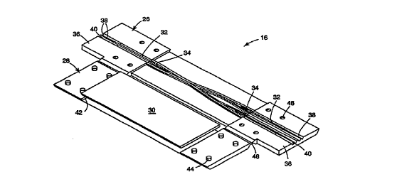
With further l~;re~t;nce to Figure 2, splice/waveguide Ple~nPnt 16, shown
in an ...~cc~s...l-led state, is described in further detail. In one embodiment of coupler
10, ~1- ....P~ 16 co~-lp-ises three plates 26, 28 and 30 (preferably flat and~ rect~n~ r).
The bottom plate 26 has two splice areas, one at each end, with V-shaped, fiber
~ AlignmPnt grooves 32 formed therein, and a central portion having a waveguide
30 e1emPnt in~ ing waveguide chA~ lC 34. Bottom plate 26 also has c,~ . on.c or
porch areas 36 with V-shaped, fiber-receiving grooves 38 formed therein. Fibers that
CA 02207705 1997-06-11
W O96121875 PCTnUS95/15406
-10-
are inserted into the splice typically have a buffer coating which is ~l-;~ed from the
terminal ends ofthe fibers, i.e., that portion ofthe fibers which lie in fiber ~lignmf~nt
grooves 32. Fiber-receiving grooves 38 accordingly have a ramped portions 40 which
acco..~ od~tPs the bu~led portion ofthe optical fibers so as to ~ e
s microbPn-linE of the fibers at the transition from the buffered portion thereof to the
e~yosed portion thereof, and so help avoid optical losses ~clcoçi~ted with such
microb~n-lin~ Fiber-receiving grooves 38 are also wider than fiber ~ tlm~nt grooves
32 since they accommodate the burr~;r~d portion of the fibers. Those skilled in the art
will al~p- ~.,iale that the shape of grooves 32 and 38 are not limited to "V" cross-
o sections, but in the prefe,lc;d embodiment the grooves are V-shaped and have an
interior angle of a~)p,uxi~llalely 60~. In this manner, when a fiber is placed in one of the
grooves and e1~m~:nt 16 iS assembled into the module housing, the points of contact
between plates 26 and 30 and the fiber generally form an equilateral triangle which
,,~i.,i.,,;,eC transverse offset ofthe fiber and thus further reduces signal loss.
Top plate 28 has a recess 42 which accommodates cover plate 30 when
the plates are in the assembled state and cover plate 30 is interposed between bottom
plate 26 and top plate 30. Top plate 28 may be partially secured to, and aligned with,
bottom plate 26 may any convenient means, such as pegs 44 formed on top plate 28which mate with holes 46 formed on bottom plate 26. In this assembled position, one
or more fibers inserted into element 16 may be secured by sliding wedges 18, res -ltin
in a cl~mrinE force on the fibers due to the tapered shape ofthe wedges. Wedges 18
are adv~nt~geo~cly located ~dj~cPnt fiber ~lignm~nt grooves 32 so that they apply
more cla,llph~g force near the w~veguide r-h~nnPl/fiber interface than at the central
portion of e1~ment 16. Of course, wedges 18 may be ~ct~ted int1epPn-1Pntly, and so
coupler 10 may be spliced initially at only one end, such as for pi~t~iling and the other
splice completed later in the field.
Bottom plate 26 may be microreplicated from any durable m~tPri~l
pler~-ably one which is s~ffi~iently hard to avoid excess derullllalion ofthe grooves
when the fibers are clamped therein, jncllldinE materials from the group con.~ictinE of
polymers, halop,~ led polymers, polymer/ceramic composites, or cel~nics, jnclll~ing
sp~e.ll, optical quality glass. Microrepliç~tion is acco..-pli~l~Pd using methods
CA 02207705 1997-06-11
W O96/21875 1~ 5406
which include injection molding, transfer mr)kling embossing, or cast-a~d-cure. See,
e.g., U.S. Patent Nos. 5,311,604 and 5,343,544. It is preferable to use a material such
as halogr~nAted polymers since they typically exhibit lower optical losses. Similar
materials may be used to fill the waveguide rhAnnPlc, i.e., forming the waveguide
s cores. Top plate 28 may be, but is not necess~ ily, integrally formed with bottom plate
26, and co~ e~;led thereto with a "focus hinge" 48 as described in the '787 patent.
Cover plate 30 may also be formed of the same material as bottom and top plates 26
and 30.
In the embodiment of Figure 2, the waveguide PIPmPnt formed on the
0 central portion of plate 26 is a 2x4 splitter where the two input çhAnnP.lc are split into
four output r hAnnPlc More generally, the present invention con~e---plates an n x m
coupler ~l.elein n and m are, indepen~ntly, integers having a value bel.wt:en 1 and
1024, inclusive. Other n x m configurations will become apl a-~ to those skilled in
the art, such as multiple couplers on a single waveguide PlPmPnt Similarly, di~rt.
1S types of optical modules may be provided, such as a splitter, a star coupler, a
wavelength division multiplexer, an ~tt~ml~tor, an optical filter, a phase rnodulator or
an optical tap, and even co~ tir~nc of these devices may be microreplic~Ated on a
single waveguide el~m~nt, side-by-side, end-to-end or in a variety of tree structures.
For eY~mple, Figure 3 depicts an alternative splice/waveguide PlPmPnt 1~' wherêîn two
20 2x4 splitters are fabricated side-by-sîde on a single waveguide PlemPnt Pler~lably, the
input and output grooves are on equal centers to fAr ilitAte the inlerconrlçction of a
multiplicity of fibers in a single operation.
Referring now to the enl_rged view of Figure 4, the cores of the optical
fibers may be precisely aligned with waveguide çh~nnr~ls 34 by Alignin~ the rl~n~Plc on
2s the centers ofthe V-grooves during miclol~,plir.,l;oll. For single-mode applicAtionc,
the waveguide rl~Anl~r1c are appro,.;...Atrly 8 microns wide and deep, wi.th the V-
groove formed to align the optical axis of the fiber and waveguide channel with an
accuracy on the order of 0.5 micron. While the fiber AlignmPnt grooveJchannel
intPrfAr,e is shown as a surface pe~ rliYllAr to the fiber axis, it may ~llr~ ;vely be
30 'molded at a slight angle from the perpr~nrlic~ r~ say 3 to 10 degrees, to reduce back
relleclions at the interface to less than -50 dB for typical molded polymeric materials
CA 02207705 1997-06-11
W O 96/21875 PCTrUS95/15406
-12-
over a te.l.pe al~lre range of ~10 to +75 ~C. Index m~t~hing gel may optionally be
used to further decrease insertion losses. Also shown in Figure 4 are flow r.h~nnPI~ 50
which may receive excess liquid monomPr during the channel-forming process as
explained further below.
s In Figures 24, all fiber insertion grooves, fiber ~lignmPnt grooves, and
wav~ ~ide ch~nnPI~ are molded on the bottom plate 26, with the top plate 28
incorporating recess 42 for cover plate 30. Figures 5 and 6 depict another
embodiment 16" ofthe sp1ice/waveguide ~k~ .l of the present invention wherein
fiber insertion grooves 38 and ramps 40 are molded on top plate 28, with fiber
0 alignm~nt grooves 32 and waveguide ch~nnP1c 34 still molded on bottom plate 26.
Fibers inse:l led into grooves 38 are guided up ramps 40 and into ~lignm~nt grooves 32
where they are aligned with waveguide ch~nn~l~ 40. A partial view of the assembled
splice/waveguide plPmPnt 16" is shown in Figure 6 which illustrates the relationship of
the fiber insertion grooves, rarnp and fiber ~lignm-pnt grooves, and the bottom, top and
cover plates.
Yet another embodiment 16"' ofthe splice/wav~;uide P1emPnt ofthe
present invention in shown in Figures 7 and 8. In Pl~mPnt 16"', fiber ~li nmPnt
grooves 32 are formed in both bottom plate 26 and top plate 28, and are aligned by
pegs 44 and holes 46. Figure 8 reveals how, in this embodiment, waveguide .~h~ lc
34 are formed with a top surface which is coplanar with the top surface of V-grooves
32. Ch~nn~lc 34 are preferably molded only in bottom plate 26, with fiber z~lignmPnt
grooves formed so as to center the fiber axis to the opt;cal axis of the waveguide
~.11AI~ i.e., the V-grooves on bottom 26 are only slightly deeper than those on top
plate 28. The ch~nnPllgroove intPrf~e may again be molded at angle to reduce back
2s reflections. Index ~ <~ e gel may also be prelo~ded at the intP.rf~ce Fibers whose
terminal ends are beveled may be positic-mPd against ch~nnels 34 and exhibit acceptable
losses without gel if direct contact belween the fiber core and the channel is achieved.
All of the ~.~o~ embodiments of the splice/wav~uide e1em~nt
p,~rer~bly use waveguide rh~nnPI~ 34 which are formed by poly...~ a monomer in
30 situ. Following molding of the splice/waveguide elPmpnt using the desired material,
inserts (not shown) are placed into bottom plate 26, seated against the op~,~,n~,~ to the
-
CA 02207705 1997-06-11
W O96/21875 ~'CTrUS95/15406
wav~;guide cll~nn~lC These inserts are shaped to fit fiber-receiving grooves 38 and
fiber ~ nmPnt grooves 32. A liquid monom~r, such as a fluo~ à~ed acrylate, or other
curable m~teri~l, is applied to the waveguide ch~nnPlc to form cores therein. Cover
plate 30 is placed firmly onto bottom plate 26, centered on the central portion thereof
rO.. "~ the waveguide PlF.~r.. ~ As cover plate 30 is pressed onto bottom plate 26,
residual lllOI~ dl is forced out of the ~ v~guide ctl~nnplc and into flIDW çh~nn~lc 50.
This allows the ~I~AI~F1C to be filled to a precise depth without residual m~te i~l
~lll~ing a thin layer above the channel w~vG~-;rles The liquid mnnmn~ or other
material is cured to form the cores of the waveguide ch~nnplc and causes plates 26 and
10 30 to adhere to each other. The inserts are removed from the fiber-receiving and fiber
:~li~mPnt grooves. Top plate 28 is placed (hinged) on top of cover plate 30, with
pîate 30 fitting into recess 42, and pegs 44 fitting into holes 46.
Although the depicted w~ivG~.Iide cl~ n~lc 34 are shown with the same
width, ~ . ;"p widths may be microreplicated on a single wavG~Ilide P1ernpnt For15 ;..~ .P Y-bl~lches which divide a single channel into two c~ elC of di~GIill~widths are known to provide unequal splitting of the optical signal be~wGen the t~-vo
output ..I.~ c In addition, surface corrugation waveguide gratings may also be
~l~lcl~Gplicated in the same waveguide ~l~mPnt as the channel wave~idPc to provide
both broDdb~n-l and l~-u~I,alld optical filt~ring which can effect optical wavelength
20 m~
Although the invention has been desclil)ed with reference to specific
e.-.bo-l;~ s this clesr-rirtion is not meant to be construed in a limiting sense. Various
modifications of the disclosed embodiment, as well as altelllative embodimPntc of the
invention, will become appa~nl to persons skilled in the art upon reference to the
25 description ofthe invention. For ~ .plc fiber stubs could be prPloaded in thesplice/waveguide PlenlPnt~ in the fiber-recei-ving grooves, aligned with lthe wavd ~lide
cores and held in place by epoxy or other curable materials, in~ ing polymers and
ceramics; these ffber stubs would then be spliced to the input and OUtpllt fibers. It is
~hel1rurt; c~ e~..rl~ted that such mo-lificatinnc can be made willloul departing from
30 the spirit or scope ofthe present invention as defined in the appended claims.