Note: Descriptions are shown in the official language in which they were submitted.
CA 02207745 1997-06-13 .
WO 96/19048 PCT/US95116002
METHOD AND APPARATUS FOR INCREASING RECEIVER
ITY TO INTERFERENCE
BACKGROUND OF THE INVENTION
I. FIELD OF THE INVENTION
The present invention relates to radio communications. More
particularly, the present invention relates to improving a communication
receiver's immunity to interference.
II. DESCRIPTION OF THE RELATED ART
There are presently multiple types of cellular radiotelephone
systems operating. These systems include the advanced mobile phone
system (AMPS) and the two digital cellular systems: time division
multiple access (TDMA) and code division multiple access (CDMA). The
digital cellular systems are being implemented to handle capacity
problems that AMPS is experiencing.
All the cellular radiotelephone systems operate by having multiple
antennas covering a geographic area. '~'he antennas radiate into an area
referred to in the art as a cell. The AMPS cells are separate and distinct
from the CDMA cells. This makes it likely that the antenna for one
system's cell may be located in a cell of another system. Likewise, within a
particular system (AMPS, CDMA, and TDMA), there are two service
providers within a given area. These providers often choose to place cells
in different geographical locations from their competitor, hence there are
situations where a radiotelephone on system 'A' might be far away from
the nearest system 'A' cell while close to a system 'B' cell. This situation
means that the desired receive signal will be weak in the presence of
strong multi-tone interference.
This intermixing of system antennas can cause problems for a
mobile radiotelephone that is registered in one system, such as the CDMA
system, and travels near another system's antenna, such as an AMPS
antenna. In this case, the signals from the AMPS antenna can interfere
with the CDMA signals being received by the radiotelephone due to the
proximity of the radiotelephone with the AMPS cell or the higher power of
the AMPS forward link signal.
The multi-tone interference encountered by the radiotelephone from
the AMPS signals creates distortion products or spurs. If these spurs fall
CA 02207745 1997-06-13
WO 96/19048 PCT/US95/16002
2
in the CDMA band used by the radiotelephone, they can degrade receiver
and demodulator performance.
It is frequently the case in an AMPS system for the carriers (A and
B bands) to 'jam' the competitor system unintentionally. The goal of the
cellular carrier is to provide a high signal to noise ratio for all the users
of
their system by placing cells close to the ground, or near their users, and
radiating the FCC power limit for each AMPS channel. Unfortunately,
this technique provides for better signal quality for the carrier's system at
the expense of interfering with the competitor's system.
Intermodulation distortion, such as that caused by the above
situations, is defined in terms of the peak spurious level generated by two
or more tones injected into a receiver. Most frequently, the third-order
distortion level is defined for a receiver in terms of a third-order input
intercept point or IIP3. IIP3 is defined as the input power (in the form of
two tones) required to create third order distortion products equal to the
input two tone power. As shown in FIG. 13, IIP3 can only be linearly
extrapolated when a non-linear element, such as an amplifier, is below
saturation.
As shown in FIG. 14, third-order distortion products occur when
two tones are injected in a receiver. Tone #1 is at frequency fl at power
level P1 in dBm. Tone #2 is at frequency ~ at power level P2 in dBm.
Typically P2 is set to equal P1. Third-order distortion products will be
created at frequencies 2xf1 - ~ and 2xf2 - fl at power levels P12 and P21
respectively. If P2 is set to equal P1, then spurious products should be
equal, or P12 and P21 should be equal. Signal fc is injected at power level
Pc to show that the added distortion is equal to a low level signal in this
case. If there is a filter that filters out fl, f2 and ~1 after the distortion
is
created, the power at f12 will still interfere with the signal power at fc. I
n
example FIG. 14, for a CDMA application, the goal is that the intermod
P12 should be equal to the signal power of -105 dBm for a total two tone
power of -43 dBm, so the IIP3 must be > -9 dBm.
As is well known in the art, IIP3 for a single non-linear element is
defined as the following:
IIP3 = I 2 3 + Pin (dBm)
If Pl = P2, then Pin = P1 + 3 dB or P2 + 3 dB (dBm) and
IM3=Pl-Pi2=P2-P2~=P2-P12=Pm P21(dB)
CA 02207745 1997-06-13
WO 96/19048 PCT/US95/16002
For cascaded IIP3, where more non-linear elements are used,
the equation is as follows:
. IIP3 = -10*1og10(10(Gain - element IIP3)/10 -~ lO(-IIP3 of previous
stages)/10~
where: Gain = gain to element input.
Therefore, one way to improve the cascaded IIP3 of a receiver is to
lower the gain before the first non-linear element. In this case, the LNA
and mixer limit IIP3. However, another quantity needs to be defined that
sets the sensitivity or lowest receive signal level without interference. This
quantity is referred to in the art as the noise figure (NF). If the gain of
the
receiver is reduced to improve IIP3 (and interference immunity), the NF
(and sensitivity to small desired signals) is degraded.
The Element NF is defined as the following:
Element NF = Ni ' No (~) '
where: Ni is the input signal to noise ratio in dB, and
So
No is the output signal to noise ratio in dB:
For elements in cascade in a receiver, the equation is as follows:
lO(NFe/10~- 1
Cascaded NF = 10*1og10 ( lO~NFi/10) -~.
I O( G°in / 10 ~
where: NFe equals the noise figure of the element,
NFi equals the cascaded noise figure up to the element, and
Gain equals the running gain up to the element.
The 'best' cascaded NF can be achieved if the gain up to the element
is maximized, this equation is in contradiction to the requirement for the
'best' cascaded IIP3. For a given element by element and receiver NF and
IIP3, there are a limited set of gain values for each element that meet all
of the requirements.
Typically, a receiver is designed with NF and IIP3 as predefined
a
constants, as both of these quantities set the receiver's dynamic range of
operation with and without interference. The gain, NF, & IIP3 of each
' device are optimized based on size, cost, thermal, quiescent and active
element current consumption. In the case of a dual-mode CDMA/FM
portable cellular receiver, the CDMA standard requires a 9 dB NF at
minimum signal. In other words, for CDMA mode, the sensitivity
CA 02207745 1997-06-13
WO 96/19048 PCT/US95/16002
4
requirement is a 0 dB S/N ratio at -104 dBm. For FM mode, the
requirement is a 4 dB S/N ratio at -116 dBm. In both cases, the
requirements can be translated to a NF as follows:
NF = S (dBm) - N (dB) - Ntherm (dBm/Hz) - Signal BW (dB/Hz),
where S is the minimum signal power,
S is the minimum signal to noise ratio,
N
Ntherm is the thermal noise floor (-174 dBmlHz C~ 290° K),
and Signal BW (dBlHz) is the bandwidth of the signal.
Therefore,
CDMA NF = -104 dBm - 0 dB - (- 174 dBm/Hz) - 61 dB/Hz = 9 dB,
FM NF = -116 dBm - 4 dB - (- 174 dBm/Hz) - 45 dB/Hz = 9 dB,
where -61 dBm/Hz is the noise bandwidth for a CDMA channel
-45 dBm/Hz is the noise bandwidth for a FM channel
However, the receiver's NF is only required when the signal is near
the minimum level and the IIP3 is only required in the presence of
interference or strong CDMA signals.
There are only two ways to provide coverage in the areas where the
carrier is creating strong interference. One solution is to employ the same
technique; i.e., co-locate their cells along with the competition's. Another
solution is to improve the immunity of a receiver to interference. One way
to improve the immunity is to increase the receiver current. This is not a
practical solution, however, for a portable radio that relies on battery
power. Increasing the current would drain the battery more rapidly,
thereby decreasing the talk and standby time of the radiotelephone. There
is a resulting need to minimize mufti-tone interference in a
radiotelephone without impacting the current consumption.
SUMMARY OF THE INVENTION
The process of the present invention adjusts attenuation in a circuit,
thereby improving a receiver's immunity to interference. The circuit has
an attenuator with attenuation and automatic gain control (AGC) with a
variable gain. The process varies the attenuation by a predetermined
amount. The gain of the circuit is then detected. If the detected gain
change is greater than a predetermined threshold, intermodulation
CA 02207745 2004-03-31
74769-85
products have been detected and the front end attenuation is
increased to reduce the intermodulation product power.
According to one aspect the invention provides an
apparatus to increase a radio receiver's immunity to radio
5 frequency interference, the radio receiver receiving a
signal, the apparatus comprising: a first switch coupled to
the received signal, the first switch having a first
position and a second position, the second position being
coupled to a bypass path; a first amplifier, coupled to the
first position of the first switch, for amplifying the
received signal; a second switch having a first position and
a second position, the first position coupled to the first
amplifier and the second position being coupled to the
bypass path; a controller coupled to the first switch and
the second switch, the controller switching the first and
second switches to the second positions in response to the
received signal exceeding a predetermined power level; a
filter coupled to the output of the first amplifier, the
filter outputting a filtered received signal at a filter
output; an oscillator for generating an oscillator signal
having a predetermined frequency; a mixer, having a first
input and a second input, the first input being coupled to
the filter output and the second input being coupled to the
oscillator, the mixer generating a downconverted signal in
response to the oscillator signal and the filtered received
signal; a second amplifier coupled to the downconverted
signal; a third amplifier coupled to the downconverted
signal; a first surface acoustical wave filter, coupled to
the second amplifier, for generating a signal for use in a
digital radiotelephone system; and a second surface
acoustical wave filter, coupled to the third amplifier, for
generating a signal for use in an analog radiotelephone
system.
CA 02207745 2004-03-31
74769-85
5a
According to another aspect the invention provides
an apparatus to increase a radio receiver's immunity to
radio frequency interference, the radio receiver receiving a
signal, the apparatus comprising: a switch coupled to the
received signal, the switch having an open position and a
closed position, the closed position being coupled to a
bypass path; a first amplifier having an input coupled to
the switch and an output coupled to the bypass path; a
controller coupled to the switch, for switching the switch
to the closed position in response to the received signal
exceeding a predetermined power level; a filter coupled to
the output of the first amplifier, the filter outputting a
filtered received signal at a filter output; an oscillator
for generating an oscillator signal having a predetermined
frequency; a mixer, having a first input and a second input,
the first input being coupled to the filter output and the
second input being coupled to the oscillator, the mixer
generating a downconverted signal in response to the
oscillator signal and the filtered received signal; second
amplifier coupled to the downconverted signal; a third
amplifier coupled to the downconverted signal; a first
surface acoustical wave filter, coupled to the second
amplifier, for generating a signal for use in a digital
radiotelephone system; and a second surface acoustical wave
filter, coupled to the third amplifier, for generating a
signal for use in an analog radiotelephone system.
According to yet another aspect the invention
provides an apparatus to increase a radio receiver's
immunity to radio frequency interference, the radio receiver
receiving a signal, the apparatus comprising: a first
amplifier, having an input coupled to the received signal,
for generating an amplified received signal at an output; a
bypass path coupled to the input of the first amplifier; a
CA 02207745 2004-03-31
74769-85
5b
switch having a first position and a second position, the
first position coupled to the first amplifier output and the
second position being coupled to the bypass path; a
controller coupled to the switch, for switching the switch
from the first position to the second position in response
to the received signal exceeding a predetermined power
level; a filter coupled to the output of the first
amplifier, the filter outputting a filtered received signal
at a filter output; an oscillator for generating an
oscillator signal having a predetermined frequency; a mixer,
having a first input and a second input, the first input
being coupled to the filter output and the second input
being coupled to the oscillator, the mixer generating a
downconverted signal in response to the oscillator signal
and the filtered received signal; a second amplifier coupled
to the downconverted signal; a third amplifier coupled to
the downconverted signal; a first surface acoustical wave
filter, coupled to the second amplifier, for generating a
signal for use in a digital radiotelephone system; and a
second surface acoustical wave filter, coupled to the third
amplifier, for generating a signal for use in an analog
radiotelephone system.
According to still another aspect the invention
provides a receiver circuit for increasing immunity of a
radiotelephone to radio frequency interference, said
radiotelephone having an antenna for receiving and
transmitting radio signals, a duplexer coupled to said
antenna, and a signal processing circuit coupled to said
duplexer, the receiver circuit comprising: a receive
amplifier, having an input and an output, said receive
amplifier for amplifying said received radio signals; a
bypass path, switchably coupled to said receive amplifier,
said bypass path for attenuating a gain of said receive
CA 02207745 2004-03-31
74769-85
5c
amplifier when in a shunt position; a controller, coupled to
said bypass path, for switching said bypass path to said
shunt position when a detected power level of said received
radio signals exceeds a predetermined threshold; filter
coupled to the output of the receive amplifier, the filter
outputting a filtered received signal at a filter output; an
oscillator for generating an oscillator signal having a
predetermined frequency; a mixer, having a first input and a
second input, the first input being coupled to the filter
output and the second input being coupled to the oscillator,
the mixer generating a downconverted signal in response to
the oscillator signal and the filtered received signal; a
second amplifier coupled to the downconverted signal; a
third amplifier coupled to the downconverted signal; a first
surface acoustical wave filter, coupled to the second
amplifier, for generating a signal for use in a digital
radiotelephone system; and a second surface acoustical wave
filter, coupled to the third amplifier, for generating a
signal for use in an analog radiotelephone system.
BRIEF DESCRIPTION OF THE DRAWINGS
FIG. 1 shows a block diagram of the apparatus of
the present invention for increasing receiver immunity.
FIG. 2 shows a block diagram of another alternate
embodiment of the present invention.
FIG. 3 shows a block diagram of another alternate
embodiment of the present invention.
FIG. 4 shows a block diagram of another alternate
embodiment of the present invention.
CA 02207745 2004-03-31
74769-85
5d
FIG. 5 shows another plot of received RF input
power versus carrier to noise ratio in accordance with the
embodiment of FIG. 7.
FIG. 6 shows a plot of receive RF input power
versus carrier to noise ratio in accordance with the
embodiment of FIG. 8.
FIG. 7 shows a block diagram of another alternate
embodiment of the present invention.
FIG. 8 shows a plot of interference power vs.
signal power without using the apparatus of the present
invention.
FIG. 9 shows a plot of interference power vs.
signal power in accordance with the alternate embodiments of
the apparatus of the present invention.
FIG. 10 shows a block diagram of an alternate
embodiment of the present invention.
FIG. 11 shows a block diagram of another alternate
embodiment of the present invention.
FIG. 12 shows a block diagram of another alternate
embodiment of the present invention.
FIG. 13 shows a plot of non-linear transfer
characteristics and distortion measurement.
FIG. 14 shows a spectral description of distortion
products.
FIG. 15 shows a block diagram of a method for
CA 02207745 2004-03-31
74769-85
5e
detecting the power of a received signal in accordance with
the present invention.
FIG. 16 shows a flow chart of the attenuation
control process of the present invention.
CA 02207745 1997-06-13
WO 96/19048 PCT/US95/16002
6
DESCRIPTION OF THE PREFERRED EMBODllVIENT
It is an objective of the present invention to vary the receiver NF and
IIP3 for enhancing the IIP3 (or interference immunity) without
compromising NF when necessary. This performance 'enhancement' is
accomplished by varying the gain of the first active element in the
receiver. The gain can be varied by varying the gain of the LNA over a
continuous range or switching out the low noise amplifier with bypass
switches.
A block diagram of the preferred embodiment of the present
invention is illustrated in FIG. 1. This embodiment involves adjusting the
LNA 115 gain on a continuous basis using adjustable gain control (AGC )
110 at the receiver front end. The continuous AGC 110 at thefront end also
provides a linearity benefit at a minimum RF input level while the AGC
120 on the transmit side may reduce the IF AGC 125 and 130
requirements.
This embodiment detects the power output from the LNA 115. The
power detector 105 measures both the signal power and the jammer power
together at RF. Using this embodiment, the power detector 105 can
continuously decrease the LNA 115 gain at a lower received power than
the -65 dBm of the subsequent "switched gain" embodiments of FIGs. 7, 10,
11 and 12.
The preferred embodiment operates by the power detector 105
detecting the received signal and jammer power at RF. This detected
power goes through a loop filter and is used to adjust the receive AGC 110,
thereby adjusting the intercept point of the receive components. The gain
is decreased as the measured power increases and the gain is increased
as the measured power decreases. This embodiment could also combine
the LNA 115 and the AGC 110 to form a variable gain LNA, thus
eliminating the need for the separate AGC 110 block. The power of the
transmit AGC 120, located before the power amplifier 150, is adjusted in
the same way as the receive AGC 110in order to maintain the overall TX
power level.
AGC amplifiers 125 and 130 are also located after the mixers 135
and 140 in order to adjust the gain after the jammers have been filtered out
by the bandpass filter 145. These AGC amplifiers 125 and 130 perform the
normal CDMA AGC function of open loop power control, closed loop power
control, and compensation. These IF AGCs 125 and 130 are required due
to the wide dynamic range requirements for CDMA. Typically, these
CA 02207745 1997-06-13
WO 96/19048 PCT/US95116002
AGCs I25 and 130 have greater than 80 dB of gain range. The receive and
transmit AGC 125 and 130 after the mixers are adjusted by another power
detector 150 that measures the total power after the received signal is
downconverted. The power detector 150 adjusts the AGCs 125 and 130 gain
downward as the downconverted signal's power increases and adjusts the
AGCs 125 and 130 gain upward as the downconverted signal's power
decreases.
In the preferred embodiment, the received signals are in the
frequency band of 869-894 MHz. The transmitted signals are in the
frequency band of 824-849 MHz. Alternate embodiments use different
frequencies.
The plot illustrated in FIG. 5 shows the benefit of this AGC
approach. The left hand y-axis shows the carrier over noise ratio versus
receive input power parameterized by the jammer level. The right hand y-
axis shows the total jammer power required for a constant C/J as a
function of received input power. When the jammer is not present (-100
dBm), the radio operates as though there is no RF AGC. As the jammer is
increased, the C/N is decreased, but the effective linearity is also
increased. In this example, the RF dynamic range -is 30 dB and the
threshold, where the RF AGC becomes active, is at the point the jammer
power is greater than -25 dBm.
An alternate embodiment of the continuous gain adjustment is
illustrated in FIG. 2. This embodiment first filters out the jammers with
the bandpass filter 205 before the power detector 210 determines the power
level of the downconverted signal. A threshold detector 225 determines
when the signal power level reaches a certain point, -105 dBm in this
embodiment, and then adjusts the AGCs 230 and 235 gain down when the
signal power exceeds that power level. The AGCs 230 and 235 gain is
adjusted upward when the signal power level goes below this threshold.
The gain of AGCs 215 and 220 after the mixers 240 and 245 is adjusted
continuously without checking for a predetermined threshold of power,
performing the normal CDMA AGC power control.
. The plot of this embodiment is illustrated in FIG. 6. When the
threshold is set at -105 dBm, the minimum receive RF level, the C/N does
. 35 not increase as quickly as the case where there is no RF AGC. The
advantage of this embodiment is that the linearity benefit begins at a very
low RF input power, no receive RF power detector is needed, and the AGC
loop detects signal power only. Hence, the AGC loop is a simpler design
than detecting at RF power.
CA 02207745 1997-06-13
WO 96/19048 PCT/US95/16002
Still another embodiment of the present invention is illustrated in
FIG. 3. This embodiment operates similarly to the embodiment of FIG. 1.
The only difference being the placement of the AGC 301 prior to the LNA
305 in the receive path.
Yet another embodiment of the present invention is illustrated in
FIG. 4. This embodiment uses an attenuator 405 between the antenna 410
and the duplexer 415. The attenuation is controlled by the power detector
420 after the LNA 425. The power detector 420 measures the received
signal and jammer power, filters it, and compares it to a predetermined
threshold. In this embodiment, the threshold is -25 dBm. When the
combined signal and jammer power reaches this threshold, the
attenuation caused by the attenuator 405 is increased. This adjustment
can be either in digital fixed steps or continuously adjusted. The AGC 430
and 435 after the mixers 440 and 445 are adjusted in the same manner as
the FIG. 1 preferred embodiment.
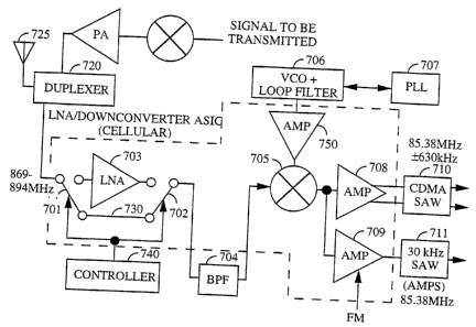
An alternate embodiment of the apparatus of the present invention
is illustrated in FIG. 7. This embodiment uses switches ?01 and ?02 to
alter the front end gain. The actual switching level depends on the signal
to noise requirements as a function of the signal level, or noise figure, for
a particular CDMA radiotelephone design. The present invention cam be
used in an AMPS radiotelephone, however the switching characteristics
will be changed to accommodate a different operating point.
This embodiment is comprised of an antenna 725 that receives and
transmits radio signals. Receive and transmit paths in the radio are
coupled to the antenna ?25 through a duplexer 720 that separates the
received signals from the transmitted signals.
A received signal is input to an LNA 703 that is coupled between two
switches ?01 and 702. One switch 701 couples the LNA 703 to the duplexer
?20 and the second switch ?02 couples the LNA 703 to a band-pass filter
704. In the preferred embodiment, the switches ?Ol and ?02 are single-pole
double-throw gallium arsenide switches.
The LNA 703 is coupled to one pole of each switch such that when
both switches 701 and 702 are switched to those poles, the received signal is
coupled to the LNA 703 and the amplified signal from the LNA 703 is
output to the band-pass filter ?04. The band-pass filter 704 in this
embodiment has a frequency band of 869-894 MHz. Alternate embodiments
use different bands depending on the frequencies of the signals being
received.
CA 02207745 1997-06-13
WO 96/19048 PCT/US95/16002
A bypass path 730 is coupled to the other pole of each switch. When
the switches 701 and 702 are switched to their other poles, the received
signal from the duplexer 720 bypasses the LNA 703 and is conducted
directly to the band-pass filter 704. In this embodiment, these switches 701
and 702 are controlled by the radiotelephone's microcontroller 740. In an
. alternate embodiment, a separate controller is used to control the positions
of these switches.
After the band-pass filter 704 has filtered the received signal, the
filtered signal is downconverted to a lower intermediate frequency (IF) for
use by the rest of the radio. The down-conversion is done by mixing 705 the
received signal with another signal having a frequency set by a phase
locked loop 707 driving a voltage controlled oscillator 706. This signal is
amplified 750 before being input to the mixer 705.
The downconverted signal from the mixer 705 is input to the back
end AGCs 708 and 709. These AGCs 708 and 709 are used by the
radiotelephone for closed loop power control, as is already well known in
the art.
In the process of the present invention, the microcontroller 740
monitors the power of the received signal. When the power exceeds -65
dBm, the microcontruller 740 instructs the switches 701 and 702 to s w itch
to the bypass position, thus coupling the received signal directly to the
bandpass filter 704. By bypassing the LNA 703 gain, the intercept point for
the receiver is increased proportionally by the reduction in gain in dB.
Alternate embodiments use other circuitry and methods to monitor the
power of the received signal.
An alternate embodiment of the process . of the present invention
continuously adjusts the front end gain. This embodiment uses a lower
power threshold such as -25 dBm.
The plots of FIGs. 8 and 9 illustrate the benefits of the switchable
gain embodiments of the present invention illustrated in FIGs. 7, 10, ll
and 12. FIG. 8 illustrates a plot of interference power versus radio
frequency (RF) signal power for a typical radio that is not using the
switchable gain apparatus. This plot shows that the maximum
interference level is limited to the receiver input compression point at -10.5
dBm. Both the single and dual tone power curves are shown.
The plot of FIG. 9 shows the interference power received by the radio
versus the radio frequency signal power received by the radio using the
switchable gain method and apparatus of the present invention. It can be
seen that at the -65 dBm point of the graph, the switches are switched to
CA 02207745 1997-06-13
WO 96/19048 PCT/US95/16002
bypass the LNA gain thus allowing a greater interference power to be
tolerated without affecting the RF signal power. Both the single tone and
two tone power curves are shown.
Another alternate embodiment of the apparatus of the present
invention is illustrated in FIG. 10. This embodiment uses a single-pole
single-throw switch 1001. In this embodiment, the switch 1001 is switched '
to the bypass path 1010 by the controller 1020 when the received signal
power reaches -65 dBm. This effectively shorts out the LNA 1002 gain, thus
coupling the received signal directly to the band-pass filter 1003.
Yet another alternate embodiment of the apparatus of the present
invention is illustrated in FIG. 11. This embodiment uses a single-pole
single-throw switch 1105 that, when closed, shorts the input of the LNA
1110 to ground through a resistor 1101. This creates an impedance
mismatch at the input causing the signal to attenuate, thus reducing the
gain caused by the LNA 1110. As in the above embodiments, the switch
1105 is closed when the input signal power reaches -65 dBm. The
resistance required for the resistor 1101 is dependent on the amount of
attenuation desired. This resistance will be different for different LNA's in
alternate embodiments.
Still another embouiment of the apparatus of the present invention
is illustrated in FIG. 12. This embodiment uses a single-pole double-throw .
switch 1201 at the output of the LNA 1205. The LNA 1205 is connected to
one pole of the switch 1201 and a bypass path 1210is connected to the other
pole. The input to the bypass path 1210 is connected to the input ofthe LNA
1205. When the power level of the received RF signal reaches -65 dBm, the
switch 1201 is thrown from the position coupling the LNA 1205 to theband-
pass filter 1220 to the bypass path 1210. This couples the signal directly to
the band-pass filter 1220, bypassing the gain of the LNA 1205.
In all of the above embodiments, the LNA can be powered down at
the same time that it is bypassed by the switch or switches. This can be
accomplished by connecting the LNA's power pin to a switch that is also
controlled by the controller. Once the LNA is bypassed and is no longer
used, power can be removed. This reduces the power consumption of the
radio, thus increasing the talk and standby time for which the battery can
be used. -
In another embodiment of the present invention, E~/Io detection is
used to determine when to adjust the front end gain. Additional
embodiments use other quality measurements, such as Eb/Io .
CA 02207745 1997-06-13
WO 96/19048 PCT/LTS95/16002
11
These ratios are quality measurements for digital communications
system performance. The Ee/Ia ratio expresses the energy per bit to the
total interference spectral density of the channel while the E~/Io ratio
expresses the energy per CDMA chip relative to the total interference
spectral density. F~/Io can be considered a metric that characterizes the
performance of one communication system over another; the smaller the
required Eb/Io the more efficient is the system modulation and detection
process for a given probability of error. Given that E~/Io and received signal
strength are readily available, the microcontroller can detect the presence
of strong interference as a drop in E~/Io while the AGC detector detects the
increased interference. The microcontroller can lower the front end gain
to improve interference immunity which would improve E~/Io and lower
the distortion products falling within the signal bandwidth.
When the signal quality goes above the F~/Io or E~/Io threshold, the
front end gain is reduced. The gain adjustment can be accomplished
using either the continuous adjustment method or the amplifier
switching method, both described above.
Still another embodiment, illustrated in FIG. 15, would be to detect
the signal power at IF or baseband instead of the combination of the signal
and jammer power at RF. T~~is approach is simpler in that there is only
one power detector and AGC control loop.
FIG. 15 illustrates a block diagram of the alternate method of
detecting the power of the received signal. The signal is first
downconverted to baseband frequency 1501. This analog signal is then
converted to a digital signal 1505 for further baseband processing
including determining the received signal strength. The chip correlator
1510determines the energy per chip with respect to the energy of all the
non-coherent components. This information, along with the received
signal strength indicator (RSSI) is used by the processor 1515 to determine
the amount of gain adjustment for both the receive 1520 and transmit 1530
power.
Since the received signal power measurement includes both the
signal and jammer power, the receive gain is increased only when both
the signal level and the energy per chip drops. Since the RSSI is being
. 35 changed, the transmit power must also be changed to compensate, thus
enabling the open loop power control to operate properly. Thus, the
processor adjusts the transmit gain whenever the receive gain is adjusted.
CA 02207745 1997-06-13
WO 96/19048 PCTILTS95/16002
Other embodiments use erasures or signal power to control the
variable gain AGC. Additional embodiments, instead of controlling both
transmit and receive power, only control receiver power.
A process for controlling the gain of the above embodiments is
illustrated in FIG. 16. This process is based on the relationship illustrated
in the graph of FIG. 13. In FIG. 13, one can see that as the interference
input power increases along the X axis, the intermodulation products (the
lower curve) increase faster than the interference power. Therefore, X dB
of attenuation applied at the input will result in a decrease of the IM3
intermodulation products by 3*X dB if interference is present at the
receiver input.
Typically, intermodulation products don't fall into the IF section of
the radio due to their low power. Intermodulation products outside of the
IF section of the radio do not cause receiver performance problems. Thus,
adjustment of the receiver gain is only necessary if the intermodulation
products are of sufficient power to affect the IF signal.
Referring to FIG. 16, the process of the present invention first
adjusts the input gain 1601. In the preferred embodiment, this gain
adjustment is 3 dB. However, other embodiments can use other values of
gain adjustment, such as tl~G range of 1 dB - 6 dB. The receiver processing
is then used to measure the change in the power of the received signal
1605. In the preferred embodiment, the automatic gain control processing
detects the IF signal power change. It is understood that measurement of
the change in received signal power may be accomplished at the RF or
baseband stages of the receiver as well.
If the signal power changes by approximately 3 dB, the CDMA
signal is greater than the noise floor and there are no intermodulation
products that might cause problems. Additional gain adjustment is not
needed in this case, but increasing the gain will improve receiver
sensitivity. IF signal power changes of approximately (3 ~ 0.5) dB are still
considered to be 3 dB.
If the IF signal power changes by less than 3 dB 1610, the CDMA
signal is less than the noise floor or there are no intermodulation products
that might cause problems. In this case, the AGC is only seeing a small
CDMA signal and noise. Therefore, it is necessary to increase the receiver
circuit gain 1615 and thus increase the sensitivity of the receiver.
If the IF signal power changes by more than 3 dB, the
intermodulation products are causing enough of a problem that additional
gain adjustment is necessary 1620. In the preferred embodiment, if the
CA 02207745 1997-06-13
WO 96/19048 ,~ ~ PCT/LTS95J16002
input gain was changed by 3 dB the intermodulation products will change
by 9 dB when large interference is present. In this case, the average gain
may be decreased by a small amount (e.g., 3 dB) until the process of the
present invention determines that the intermodulation products are
reduced to an acceptable level.
The process of the present invention can be used continuously,
checking for intermodulation products at a low rate. This rate is ten times
per second in the preferred embodiment. Other embodiments use the
process once per frame cycle. Still other embodiments use the process at
other rates, such as upon detection of a significant error on the forward
link.
In -summary, the method of the present invention enables a mobile
radio to travel near antennas of different systems while increasing the
radio's resistance to radio frequency interference from the other system.
1~ By decreasing the front end gain, the intercept point of the radio's
receive
circuitry increases so that the spurs from the other system's' signals will
not cause performance degradation of the receiver and demodulator.
I CLAIM: