Note: Descriptions are shown in the official language in which they were submitted.
CA 02207818 1999-OS-18
1
D E S C R I P T I O N
APPARATUS AND METHOD FOR DEMODULATING
MULTI-LEVEL SIGNAL
Technical Field
The present invention relates to an apparatus and
method for demodulating a multi-level signal of which the
amplitude is modulated by a multi-level.
Background Art
Recently, in the field of a radio communication,
multi-carrier modulation system is used to increase a data
transmission rate. For example, in Japan, in a radio
paging system which is standardized as "RCR STD-43", a
four-level FSK (Frequency Shift Keying) is adopted as a
signal modulating system. Further, in a case where data is
written in recording media such as an optical disk and so
on, the multi-carrier modulation system is used to record
the data with high density.
In order to demodulate a multi-carrier modulated
signal to digital data, generally, a multi-carrier
modulated signal is converted to a multi-level voltage
signal, that is, a PAM (Pulse Amplitude Modulation) signal
by using a frequency discriminator and so on. Then the
voltage signal is compared to plural threshold voltages.
For example, there are the following two well-known methods
for demodulating a four-level FSK modulated signal.
According to a first method, a four-level analog
CA 02207818 1999-OS-18
2
signal is reproduced from a four-level FSK signal by using
a frequency discriminator. The reproduced signal is
compared with three threshold voltages which are previously
set to demodulate to a four-level digital data.
A second method is basically similar to the first
method in which the reproduced four-level analog signal is
compared with three threshold voltages to demodulate to a
four-level digital data. The three threshold voltages are
not fixed voltages but are variable voltages interlocking
to a received signal. According to the second method, more
specifically, a maximum data voltage and minimum data
voltage are detected by a detector among four-level analog
signals reproduced by the frequency discriminator and the
detected voltages at both of levels are output. Between
two voltage output terminals of the detector, that is, one
output terminal for the maximum data voltage and the other
output terminal for the minimum data voltage, four
resistors are connected in series. 170, 50%, and 83s
voltages of a potential difference between the maximum data
voltage and the minimum data voltage are taken from the
connection points of the four resistors. These three
intermediate voltages are defined as the three threshold
voltages.
According to the first method, the three threshold
voltages are fixed respectively. Thus, when a local
CA 02207818 1999-OS-18
3
oscillator includes an offset, that is, when the frequency
of a received signal and reproduced signal is not matched
with that of the local oscillator, or when there are
variations and so on of characteristics of circuit elements
composing a frequency discriminator etc., there is a
problem that a multi-level signal can not be correctly
demodulated. That is, the four-level analog signal should
be reproduced by the frequency discriminator such that the
four levels of the signal are located by an equal interval
and at a just half point between adjacent threshold levels,
as shown in FIG. lA. However, in case there exists a local
offset, there is a problem that a total value of the
reproduced signal is shifted toward the side of high level
or low level. For example, when the total value is largely
shifted toward the side of high level, as shown in FIG. 1B,
all the signal levels get higher than a third threshold
level. The signals which should be inherently demodulated
to "10", "O1", and "00" are demodulated to "11", "10", and
"O1", so that the data can not be demodulated correctly.
Further, when there are variations etc. of the
characteristics of circuit elements, an amplitude of
a four-level reproduced (regenerated) analog signal is
distorted totally or partially. FIG. 1C shows an
example in a case that an amplitude of the four-level
analog signal is distorted totally. In this case, data
CA 02207818 1999-OS-18
4
which should be inherently demodulated to "11" and "00" is
demodulated to "10" and "O1", so that the data can not be
demodulated correctly. FIG. 1D shows an example in a case
that an amplitude of the four-level analog signal is
distorted partially. In this case, data which should be
inherently demodulated to "00" is demodulated to "O1", so
that the data can not be demodulated correctly.
According to the above-mentioned second method, the
three threshold voltages are interlocked to a received
signal to be varied. Accordingly, theoretically, in
either case there exists a local offset and an amplitude
distortion, it is possible to demodulate a multi-level
signal correctly. However, an element used for obtaining
the three threshold voltages is a resistor. Since it is
not evitable that each resistor has more or less
distortion of a resistance value, in fact, it is almost
impossible to obtain 170, 500, and 83o voltages of a
potential difference between the maximum data voltage
and minimum data voltage for the three threshold
voltages. Accordingly, it is assumed that there is an
unbalanced amplitude distortion of the four-level analog
signal reproduced by the frequency discriminator. Since
a first threshold voltage and a third threshold voltage
tend to suffer from an effect due to a variation of a
resistance value, the first and third threshold voltages
get lower than a second level of a received signal or
CA 02207818 1999-OS-18
higher than a third level of the received signal. FIG. lE
shows an example in the case that the third threshold
voltage is shifted toward the side of high level, as
illustrated by a dot-and-dash line. In this case, data
5 which must be inherently demodulated to "O1" is demodulated
to "00", so that the data can not be demodulated correctly.
Accordingly, it is an object of the present invention
to provide an apparatus and method for demodulating a
multi-level signal which can demodulate a multi-level
signal correctly without suffering from an effect due to a
variation of the characteristics of circuit elements.
A related object of the present invention is to
provide an apparatus and method for demodulating a multi-
level signal which are so resistant to an amplitude
variation as to demodulate a multi-level signal correctly
without shifting a level, even if there is a uniform or
unbalanced distortion of an amplitude.
Disclosure of the Invention
According to a first aspect of the present invention,
a multi-level signal demodulation apparatus comprises:
means for converting an input analog signal of which
amplitude is modulated by a multi-level to a digital
signal;
means for storing said digital signal which is
CA 02207818 1999-OS-18
6
obtained by said covering means;
means for calculating plural threshold data in
accordance with said digital signal which is stored in said
storing means; and
means for demodulating said digital signal which is
obtained by said converting means in accordance with the
plural threshold data calculated by said calculating means
to a signal according to a level of said digital signal.
According to this modulation apparatus, the input
analog signal of which amplitude is modulated by a multi-
level is converted to the digital signal according to the
level of the analog signal. Therefore, it is possible to
correctly demodulate a multi-level signal without suffering
from an effect due to a variation of the characteristics of
circuit elements. Further, it is possible to correctly
demodulate without shifting a level even if there is a
uniform or unbalanced distortion.
According to a second aspect of the present invention,
a multi-level signal demodulation apparatus comprises:
means for converting an input analog signal of which
amplitude is modulated by a multi-level to a digital
signal;
means for storing said digital signal which is
obtained by said converting means where a predetermined
- CA 02207818 1997-06-13
7
requirement is met;
means for calculating plural threshold data to
judge a level of said digital signal in accordance with
said digital signal which is stored in said storing
means; and
means for demodulating a newest~digital signal
which is obtained by said converting means in accordance
with the plural threshold data calculated by said
calculating means to a signal according to a level of
said digital signal, said demodulation means judging
that said predetermined requirement is met when said
digital signal is at a higher level than a maximum
threshold data or at a lower level than a minimum
threshold data among said plural threshold data, so that
it is possible to correct said digital signal stored in
said storing means by using the newest digital signal.
Accordingly, the input analog signal of which
amplitude is modulated by a multi-level is demodulated
according to the level of the analog signal after
converting the analog signal to a digital signal.
Further, when the level of the digital signal is higher
than the maximum threshold or lower than the minimum
threshold, the level of the digital signal is
discriminated. Accordingly, it is possible to correctly
demodulate without suffering from an effect due to a
variation of the characteristics of circuit elements.
Further, it is possible to correctly demodulate without
CA 02207818 1999-OS-18
8
shifting a level even if there is a uniform or unbalanced
distortion.
According to a third aspect of the present invention,
an apparatus according to the second aspect is provided,
wherein said storing means stores plural previous digital
signals which meet the predetermined requirement.
According to the third aspect, plural previous
thresholds are obtained from plural digital signals which
have a higher level than the maximum threshold or a lower
level than the minimum threshold. Therefore, it is
possible to correctly demodulate without suffering from an
effect due to a variation of the characteristics of circuit
elements. Further, it is possible to correctly demodulate
without shifting a level even if there is an uniform or
unbalanced distortion.
According to a fourth aspect of the present invention,
a multi-level signal demodulation method comprises the
following steps of:
converting an input analog signal of which amplitude
is modulated by a multi-level to a digital signal;
storing said digital signal which is obtained by said
converting step;
calculating plural threshold data in accordance with
said digital signal which is stored by said storing step;
and
demodulating said digital signal which is obtained
CA 02207818 1999-OS-18
9
by said converting step in accordance with the plural
threshold data calculated by said calculating step to a
signal according to a level of said digital signal.
Accordingly, the input analog signal of which
amplitude is modulated by a multi-level is demodulated
according to the level of the signal after converting the
analog signal to a digital signal. Therefore, it is
possible to correctly demodulate without suffering from an
effect due to a variation of the characteristics of circuit
elements. Further, it is possible to correctly demodulate
without shifting a level even if there is a uniform or
unbalanced distortion.
According to a fifth aspect of the present invention,
a multi-level signal demodulation method comprises the
following steps:
converting an input analog signal of which amplitude
is modulated by a multi-level to a digital signal;
storing said digital signal which is obtained by said
converting step where a predetermined requirement is met;
calculating plural threshold data to judge a level of
said digital signal in accordance with said digital signal
which is stored by said storing step; and
demodulating a newest digital signal which is
obtained by said converting step in accordance with the
plural threshold data calculated by said calculating
CA 02207818 1999-OS-18
step to a signal according to a level of said digital
signal, said demodulation step judging that said
predetermined requirement is met when said digital signal
is at a higher level than a maximum threshold data or at a
5 lower level than a minimum threshold data among said plural
threshold data, so that it is possible to correct said
digital signal stored by said storing step by using the
newest digital signal.
Accordingly, the input analog signal of which
10 amplitude is modulated by a multi-level is demodulated
according to the level of the signal after converting the
analog signal to the digital signal. Further, when a level
of the digital signal is higher than the maximum threshold
or lower than the minimum threshold, the level of the
digital signal is discriminated. Therefore, it is possible
to correctly demodulate without suffering from an effect
due to a variation of the characteristics of circuit
elements. Further, it is possible to correctly demodulate
without shifting a level even if there is a uniform or
unbalanced distortion.
According to a sixth aspect of the present invention,
a method according to the fifth aspect is provided, in
which said storing step comprises a substep of storing
plural previous digital signals which meet the
predetermined requirement.
According to the sixth aspect, plural threshold
values are obtained from plural previous digital signals
CA 02207818 1999-OS-18
11
having a higher level than the maximum threshold or a lower
level than the minimum threshold. Therefore, it is
possible to correctly demodulate without suffering from an
effect due to a variation of the characteristics of circuit
elements. Further, it is possible to correctly demodulate
without shifting a level even if there is a uniform or
unbalanced distortion.
Additional objects and advantages of the present
invention will be set forth in the description which
follows, and in part will be obvious from the description,
or may be learned by practice of the present invention.
The objects and advantages of the present invention
may be realized and obtained by means of the
instrumentalities and combinations particularly pointed out
in the appended claims.
Brief Description of the Drawings
The accompanying drawings, which are incorporated in
and constitute a part of the specification, illustrate
presently preferred embodiments of the present invention
and, together with the general description given above and
the detailed description of the preferred embodiments given
below, serve to explain the principles of the present
invention in which:
FIGS. lA - lE show a relationship between a standard
waveform of a received signal and a waveform having a local
offset or an amplitude distortion;
CA 02207818 1999-OS-18
12
FIG. 2 is a block diagram showing an example of a
radio receiver including a multi-level signal demodulation
apparatus of the present invention;
FIG. 3 is a block diagram showing a structure of a
demodulator portion of the multi-level signal demodulation
apparatus according to the first embodiment of the present
invention;
FIG. 4 is a block diagram showing a structure of a
demodulator portion of the multi-level signal demodulation
apparatus according to a second embodiment of the present
invention;
FIG. 5 shows a relationship between a reproduced data,
and first, second and third threshold levels of a multi-
level signal demodulation apparatus according to the second
embodiment of the present invention;
FIG. 6 is a block diagram showing a structure of a
demodulator portion of a multi-level signal demodulation
apparatus according to a third embodiment of the present
invention; and
FIG. 7 is a block diagram showing a structure of a
demodulator portion of a multi-level signal demodulation
apparatus according to a fourth embodiment of the present
invention.
Best Mode of Carrying Out the Invention
A preferred embodiment of a multi-level signal
demodulation apparatus according to the present
invention will now be described with reference to the
CA 02207818 1999-OS-18
13
accompanying drawings.
First Embodiment
FIG. 2 is a block diagram showing an embodiment of a
radio receiver including a multi-level signal demodulation
apparatus of the present invention. A radio receiver 1 has
a function for receiving a message which is used, for
example, in a radio paging system. The radio receiver 1
comprises an antenna 10, a receiver portion 11, an A/D
converter 12, a demodulator portion 13, a CPU 14, a display
portion 15, an alarm portion 16, a key input portion 17, a
message memory 18, a battery 19, a battery saver portion
20, and so on.
The antenna 10 receives a radio signal supplied
from a base station of a paging service company etc.
(not shown) and outputs the received signal to the
receiver portion 11. The radio signal from the base
station is a radio signal which is modulated with
digital data, for example, a four-level FSK signal. The
receiver portion 11 includes a frequency discriminator
etc. so that a received four-level FSK signal can be
reproduced to four-level analog data signal, that is,
four-level PAM (Pulse Amplitude Modulation) signal which
is supplied to an A/D converter 12. The A/D converter
12 digitizes the four-level analog data signal output
from the receiver portion 11 and supplies the digitized
signal to the demodulator portion 13. According to the
first embodiment, the four-level analog data signal is
CA 02207818 1999-OS-18
14
converted to an 8-bit digital data signal which is to be
output. The demodulator portion 13 compares the 8-bit
digital data signal output from the A/D converter 12 with
three threshold levels (first, second, and third threshold
levels as described below). Thereby demodulated data is
obtained in a di-bit form (2-bit unit) and output to the
CPU 14. Further, the demodulator portion 13 is also
controlled by the CPU 14.
The CPU 14 is a unit, such as a micro computer etc.
for controlling an operation of peripheral circuits
according to a program which is stored in an internal ROM.
The CPU 14 includes a character generator ROM for
outputting a character code (a character pattern for
display) corresponding to a character, a numeral, a symbol,
etc., and a RAM used as a work area in addition to the
above-mentioned ROM.
The display portion 15 comprises, for example, a
liquid crystal display panel, a display buffer, a driver,
etc. to display information such as a message etc. on the
liquid crystal display panel. The alarm portion 16 alarms
an incoming signal to a user. The alarm portion 16
comprises, for example, an LED (Light Emitting Diode) which
is lighted or blinked to alarm the incoming signal, a
speaker which sounds the alarm, a vibrator which vibrates
for the alarm, and so on. The key input portion 17
comprises input means such as a power source switch, an
operation key and so on.
CA 02207818 1999-OS-18
The message memory 18 is a memory for storing a
received message data, where the CPU 14 controls write and
read of the message data. The battery saver portion 20
controls a power supply from the battery 19 to the receiver
5 portion 11 in accordance with a signal provided from the
CPU 14 to save the battery 19 or to reduce a power
consumption of the battery 19. For example, in case of a
radio receiver in the radio paging system which is adapted
to receive only a signal supplied from the base station and
10 having the address thereof, the battery saver portion 20 is
operated to supply a power source for the receiver portion
11 only when a signal having the address thereof may be
supplied from the radio base station.
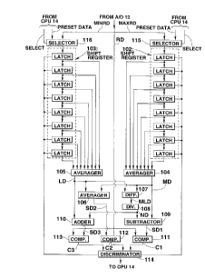
FIG. 3 is a block diagram showing a detailed
15 structure of the demodulator portion 13 shown in FIG. 2.
The demodulator portion 13 shown in FIG. 3 is an embodiment
of a multi-level signal demodulation apparatus according to
the present invention. The demodulator portion 13
comprises shift registers 102 and 103, averagers 104, 105,
and 106, a differential circuit 107, a divider 108, a
subtractor 109, an adder 110, comparators 111, 112, and
113, a discriminator 114, and selectors 115 and 116.
The shift register 102 is a register for storing M
(for example, M = 8) previous reproduced data, that is,
data which is determined as a maximum value among
CA 02207818 1999-OS-18
16
reproduced data output from the A/D converter 12 by the
discriminator 114 (described later). In the first
embodiment, eight latch circuits of 8-bit are connected in
series. The shift register 102 is connected to the A/D
converter 12 and the CPU 14 through the selector 115. The
selector 115 outputs data of an appropriate level
corresponding to a maximum value from the CPU 14 when a
power source of the radio receiver 1 is turned on or when
the battery 19 is exchanged. The selector 115 is arranged
so that the maximum data are preset in each step of the
shift register 102, that is, in eight latch circuits.
Accordingly, the shift register 102 is usually connected to
the A/D converter 12 through the selector 115. Further,
the shift register 102 is operated for shifting by pulse
signals PS1 output from the discriminator 114 when the
reproduced data from the A/D converter 12 is determined as
a maximum value. Accordingly, the reproduced data from the
A/D converter 12 is input (or is taken in) as a newest
maximum reproduced data MAXRD, and then an oldest maximum
reproduced data MAXRD is erased (is shifted out).
The shift register 103 is a register for storing M
(for example, M = 8) previous reproduced data, that is,
data which is determined as a minimum value among
reproduced data output from the A/D converter 12 by the
discriminator 114. In the first embodiment, eight latch
circuits of 8-bit are connected in series. The shift
CA 02207818 1997-06-13
~a
17
register 103 is connected to the A/D converter 12 and
the CPU 14 through the selector 116. The selector 116
outputs data of an appropriate level corresponding to a
minimum value from the CPU 14 when a power source of the
radio receiver 1 is turned on or when the battery 19 is
exchanged. The selector 116 is arranged so that the
minimum data are preset in each step of the shift
register 103, that is, in eight latch circuits.
Accordingly, the shift register 103 is usually connected
to the A/D converter 12 through the selector 116.
Further, the shift register 103 is operated for shifting
by pulse signals PS2 output from the discriminator 114
when the reproduced data from the A/D converter 12 is
determined as a minimum value. Accordingly, the
reproduced data from the A/D converter 12 is input (or
is taken in) as a newest minimum reproduced data MINRD,
and then an oldest minimum reproduced data MINRD is
erased (is shifted out).
The averager 104 is a circuit for averaging eight
previous maximum reproduced data MAXRD stored in the
shift register 102 to obtain average data MD. The
resultant data is supplied to the subtractor 109, the
differential circuit 107, and the averager 106. The
averager 105 is a circuit for averaging 8 previous
minimum reproduced data MINRD stored in the shift
register 103 to obtain average data LD. The resultant
data is supplied to the differential circuit 107, the
CA 02207818 1997-06-13
18
averager 106, and the adder 110.
The differential circuit 107 is a circuit for
obtaining a difference between average data MD from
the averager 104 and average data LD from the averager
105 to obtain differential data MLD. The resultant
data is supplied to the divider 108. The divider 108
is a circuit where differential data MLD from the
differential circuit 107 is divided by a constant "6"
which is previously set to obtain divided data ND. The
resultant data is supplied to the subtractor 109 and the
adder 110.
The subtractor 109 is a circuit for subtracting the
divided data ND from the divider 108 from the average
data MD from the averager 104 to obtain a first
threshold data SD1. The resultant data is supplied to
the comparator 111. The averager 106 is a circuit for
averaging the average data MD from the averager 104 and
the average data LD from the averager 105 to obtain a
second threshold data SD2. The resultant.data is
supplied to the comparator 112. The adder 110 is a
circuit for adding the divided data ND from the divider
108 to the average data LD from the averager 105 to
obtain a third threshold data SD3. The resultant data
is supplied to the comparator 113.
The comparator 111 is a circuit for comparing
present reproduced data RD from the A/D converter 12
with the first threshold data SD1 from the subtractor
CA 02207818 1999-OS-18
19
109 to output comparison data C1. Where, the comparison
data C1 indicates whether the present reproduced data RD is
higher than the first threshold data SD1 or not. The
comparison data C1 is supplied to the discriminator 114.
The comparator 112 is a circuit for comparing the present
reproduced data RD from the A/D converter 12 with the
second threshold data SD2 from the averager 106 to output
comparison data C2. The comparison data C2 indicates
whether the present reproduced data RD is higher than the
second threshold data SD2 or not. The comparison data C2
is supplied to the discriminator 114. The comparator 113
is a circuit for comparing the present reproduced data RD
from the A/D converter 12 with the third threshold data SD3
from the adder 110 to output comparison data C3. The
comparison data C3 indicates whether the present reproduced
data RD is higher than the third threshold data SD3 or not.
The comparison data C3 is supplied to the discriminator
114.
The discriminator 114 is a circuit for judging which
level the present reproduced data RD corresponds to in
accordance with each comparison data C1, C2, and C3 from
the comparators 111, 112, and 113.
Next, an operation of the apparatus will be explained.
A radio signal received by the antenna 10 is converted to a
four-level data signal in the receiver portion 11. The
data signal is further converted to an 8-bit digital
data signal in the A/D converter 12 to be supplied to
CA 02207818 1997-06-13
the demodulator portion 13 shown in FIG. 3. In the
demodulator portion 13, three threshold levels SDl-SD3
are calculated in accordance with eight maximum
reproduced data MAXRD which are previously stored in the
5 shift register 102 and eight minimum reproduced data
MINRD which are previously stored in the shift register
103. The first threshold data SD1 is supplied to the
comparator 111 from the subtractor 109. The second
threshold data SD2 is supplied to the comparator 112
10 from the averager 106. The third threshold data SD3 is
supplied to the comparator 113 from the adder 110.
Accordingly, each digital data signal (the reproduced
data) input from the A/D converter 12 is compared
with the threshold levels SD1, SD2, and SD3 by
15 corresponding comparators 111, 112, and 113,
respectively. Each comparator 111, 112, and 113
outputs each comparison data Cl, C2, and C3,
' ' respectively, to the discriminator 114.
In the discriminator 114, when all the comparison
20 data C1, C2, and C3 are "1", that is, when the present
reproduced data RD is a maximum data higher than the
first threshold data SD1, di-bit data "11" is supplied
to the CPU 14 as demodulation data and the pulse signal
PS1 is output. The pulse signal PS1 is supplied to the
shift register 102 as a shift pulse as described in
detail below.
In the discriminator 114, when the comparison data
CA 02207818 1999-OS-18
21
C1 is "0", and the comparison data C2 and C3 are "1", that
is, when the present reproduced data RD is lower than the
first threshold data SD1 and higher than the second
threshold data SD2, Di-bit data "10" is supplied to the CPU
14 as demodulation data. Further, when the comparison data
C1 and C2 are "0", and the comparison data C3 is "1", that
is, when the present reproduced data RD is lower than the
second threshold data SD2 and higher than the third
threshold data SD3, di-bit data "01" is supplied to the CPU
14 as demodulation data. Further, when all the comparison
data C1, C2, and C3 are "0", that is, when the present
reproduced data RD is a minimum data lower than the third
threshold data SD3, Di-bit data "00" is supplied to the CPU
14 as demodulation data and the pulse signal PS2 is output.
The pulse signal PS2 is supplied to the shift register 103
as a shift pulse.
An operation in a case where the pulse signals PS1 and
PS2 are output from the discriminator 114 is explained.
As described above, when the present reproduced data RD
from the A/D converter 12 is higher than the first
threshold data SD1, the discriminator 114 outputs the
pulse signal PS1 having a function as shift pulse of the
shift register 102. When the present reproduced data RD
from the A/D converter 12 is lower than the third
threshold data SD3, the discriminator 114 outputs the
pulse signal PS2 having a function as shift pulse of the
CA 02207818 1997-06-13
22
shift register 103.
When the shift register 102 is supplied with the
pulse signal PS1, the storage data which is stored in
each latch is shifted by one. Thus, the reproduced data
RD which is output from the A/D converter 12 and
determined as data higher than the first threshold data
SD1 by the discriminator 114 is taken in the first latch
of the shift register 102 as the newest maximum data
MAXRD. At the same time, the oldest maximum data stored
in the eighth latch of the shift register 102 is shifted
out to be erased. That is, eight maximum reproduced
data MAXRD which are output from the shift register 102
to the averager 104 are updated. Thus, the average data
MD output from the averager 104 to the subtractor 109,
the differential circuit 107, and the averager 106 is
changed. The first threshold data SD1 output from the
subtractor 109, the second threshold data SD2 output
from the averager 106, and the third threshold data SD3
output from the adder 110 are corrected, respectively.
These three corrected threshold data SD1, SD2, and SD3
are defined as threshold level when a level of next
reproduced data is determined.
Similarly, when the shift register 103 is supplied
with the pulse signal PS2, the storage data which is
stored in each latch is shifted by one. Thus, the
reproduced data RD which is output from the A/D
converter 12 and determined as data lower than the third
CA 02207818 1999-OS-18
23
threshold data SD3 by the discriminator 114 is taken in the
first latch of the shift register 103 as the newest minimum
data. At the same time, the oldest minimum data stored in
the eighth latch of the shift register 103 is shifted out
to be erased. That is, eight minimum reproduced data MINRD
which are output from the shift register 103 to the
averager 105 are updated. Thus, an average data LD output
from the averager 105 to the differential circuit 107, the
averager 106, and the adder 110 is changed. The first
threshold data SD1 output from the subtractor 109, the
second threshold data SD2 output from the averager 106, and
the third threshold data SD3 output from the adder 110 are
corrected, respectively. These three corrected threshold
data SD1, SD2, and SD3 are defined as threshold level when
a level of next reproduced data is determined.
Thus, according to the first embodiment described
above, a multi-level amplitude modulated signal such as
4PAM signal etc. is demodulated after the signal is
digitized. Further, in the following two cases, the
first, second and third threshold values are corrected
in accordance with the reproduced data RD (more
specifically, eight previous maximum and minimum data
including the reproduced data RD). One case is that the
level of the reproduced data RD is higher than the first
threshold level (maximum threshold level). The other
CA 02207818 1999-OS-18
24
case is that the level of the reproduced data RD is lower
than the third threshold level (minimum threshold level).
Accordingly, it is possible to correctly demodulate the
multi-level modulated signal without suffering from an
effect due to a variation of the characteristics of circuit
elements. Further, it is possible to correctly demodulate
the multi-level modulated signal without shifting a level
even if there is a uniform or unbalanced distortion of
amplitude.
Second Embodiment
According to the first embodiment described above,
seven arithmetic operation circuits 104-110 and three
comparators 111-113 are necessary to demodulate data.
Therefore, a circuit construction is more or less
complicated. According to the second embodiment, one full
adder and plural registers are used to demodulate data.
FIG. 4 is a block diagram showing a detailed
structure of a demodulator portion according to the
second embodiment of the present invention. In FIG. 4,
a demodulator comprises, for example, a controller 201,
registers 202, 203, 204, 206, 207, and 208, a shift
register 205, a data selector 209, a code inverter 210,
a full adder 211, a barrel shifter 212, a discriminator
213, and selectors 214 and 215. The demodulator is
adaptable to the receiver 1 shown in FIG. 2. In this
case, that is, the case of adapting the demodulator to
CA 02207818 1999-OS-18
the receiver 1 shown in FIG. 2, similarly to the
demodulator portion 13, the demodulator shown in FIG. 4 is
connected between the A/D converter 12 and the CPU 14.
In order to easily understand a demodulation
5 operation, first, a principle of the second embodiment is
explained.
As explained in the background of the invention,
when there is a local offset, all the levels of a four-
level analog signal reproduced by the frequency
10 discriminator etc. are shifted at the side of high level
or low level. When there is a variation of the
characteristics of circuit elements forming the
frequency discriminator etc., an amplitude of a
reproduced four-level analog signal is partially or
15 totally distorted. According to the first embodiment,
to solve these problems, three threshold levels are
obtained in accordance with maximum and minimum data in
the reproduced data output from the A/D converter 12.
A level of the reproduced data output from the A/D
20 converter 12 is determined in accordance with these
three threshold levels. Contrary to the first embodiment,
according to the second embodiment, the reproduced data
output from the A/D converter 12 is normalized before
demodulation. That is, the reproduced data output from
25 the A/D converter 12 is re-scaled so that an average of
the maximum value and an average of the minimum value
are "EO" and "20", respectively, by hexa-decimal
CA 02207818 1997-06-13
26
notation.
FIG. 5 shows a relationship between a distribution
of the level of the reproduced data which is output from
the A/D converter 12, normalized values thereof, and
_, 5 three threshold levels. 8-bit reproduced data RD is
noted by 256 graduation from OOg to FFg (where, H means
a hexa-decimal notation). FIG. 5 shows an example of
4PAM signal so that the level distribution includes
' four levels. Therefore, three threshold levels for
discriminating the level of the reproduced data are the
same as those used in the first embodiment. If the
average of the maximum data is represented by m and the
average of the minimum data is represented by 1, the
three threshold data (the first, second, and third
threshold data) SL1, SL2, and SL3 are represented as
follows:
DP = (m - 1)/6 (1)
SL1 = m - DP
=(5m + 1)/6 (2)
SL2 - (m + 1)/2 (3)
SL3 - 1 + DP
=(m + 51)/6 (4)
Since the reproduction data RD is normalized so
that an average of the maximum value and an average of
the minimum value are "EO" and "20", respectively, by
hexa-decimal notation, the normalized first to third
threshold data SL1, SL2, and SL3 are represented as "CO",
_ y CA~02207818 1997-06-13
27
"80", and "40" by hexa-decimal notation. After
normalization, a virtual lowest value VS (= OOg) which
is lower than the average 1 of the reproduced data from
the A/D converter 12 by a level DP is represented as
follows:
VS = 1 - DP
=(71 - m)/6 (5)
The normalized reproduced data RD, i.e., the re-
scaled data SCL is represented as follows:
SCL = (RDL - VS)/8~DP
=(RDL - (71 - m)/6)/8((m - 1)/6)
=(6RDL - 71 + m)/8(m - 1) (6)
According to the second embodiment, the reproduced
data RD from the A/D converter 12 is processed in
accordance with the above-mentioned equation (6).
The demodulator portion shown in FIG. 4 for
performing the above operation is explained in detail.
The demodulator portion 200 comprises a controller 201,
registers 202, 203, 204, 206, 207, and 208, a shift
register 205, a data selector 209, a code inverter 210,
a full adder 211, a barrel shifter 212, a discriminator
213, and selectors 214 and 215. In order to simplify an
arithmetic operation, averages of the maximum values and
minimum values are not calculated during an operation
but the total values thereof are used.
According to the above construction, the controller
201 controls the whole demodulator portion. That is,
CA 02207818 1997-06-13
_ <
28
the controller 201 controls each circuit in accordance
with a control signal CS from the CPU 14, a maximum
value detection signal MDTCT and a minimum value
detection signal LDTCT from the discriminator 213. The
registers 202 and 203 are shift registers, each storing
m maximum reproduced data MAXRD (similarly to the first
embodiment, m = 8) and m minimum reproduced data MINRD.
Each input of the shift registers 202 and 203 is
connected to the data selectors 214 and 215. Similar to
the first embodiment, an appropriate level corresponding
to the maximum value and the minimum value are preset in
the shift registers 102 and 103 by the CPU 14 when a
power source of the radio receiver 1 is turned on or
when the battery 19 is exchanged. The selectors 214 and
215 are connected to the output terminal of the A/D
converter 12. The registers 202 and 203 supply the
outputs thereof to the data selector 209. The register
204 is a shift register for storing the first threshold
data SD1, the second threshold data SD2, and the third
threshold data SD3. The first through third threshold
data SD1, SD2, and SD3 are preset by the CPU 14 and
output to the data selector 209 when the reproduced data
from the A/D converter 12 is discriminated. The first
through third threshold data SD1, SD2, and SD3 are
typically "CO", "80", and "40" in the hexa-decimal
notation, but may be determined for every receiver based
on the measured data.
CA 02207818 1999-OS-18
29
The shift register 205 stores a normalized data, that
is, an input data (reproduced data) from the A/D converter
12 which is operated as described below. The input
terminal of the shift register 205 is connected to a carry
output terminal CY of the full adder 211. The input
terminal of the shift register 205 is an inverting input.
The registers 206, 207, and 208 are registers for an
arithmetic operation, each connected to an output of the
barrel shifter 212. The outputs (12-bit, 11-bit, and 11-
bit) of the registers 206, 207, and 208 are connected to
the data selector 209. The output of the register 206 is
also connected to the full adder 211.
An input of the data selector 209 is connected to an
output of the A/D converter 12, and each output of the
registers 202, 203, 204, 206, 207, and 208, and the shift
register 205. A 12-bit output data to be supplied to the
code inverter 210 is selected by the data selector 209
under control of the controller 201. A code of the output
data from the data selector 209 is inverted or remains as
it is and then supplied to the full adder 211.
The full adder 211 is a circuit for receiving a
12-bit output data from the register 206 and a 12-bit
output data from the code inverter 210 to add them
together. The adder 211 may perform a subtraction
operation if the code inverter 210 inverts the input
CA 02207818 1999-OS-18
data. The output of the full adder 211 is connected to the
barrel shifter 212 and the shift register 205. The
operation resultant data (carry output) CY (1-bit) is
supplied to the barrel shifter 212, the shift register 205,
5 and the discriminator 213. The carry output shows whether
an operation is completed or not. An operation resultant
data (12-bit) is supplied to the barrel shifter 212.
The barrel shifter 212 is a circuit for dividing an
output of the full adder 211, that is, the addition or
10 resultant subtraction data by 2i and for multiplying the
output of the full adder 211 by 21 in a simple manner. The
barrel register 212 is connected to an output of the full
adder 211. An addition or resultant subtraction data is
output as it is or after shift-down according to mode.
15 That is, the barrel shifter 212 is set to a shift mode or
usual mode by the controller 201. In the case of the shift
mode, the operation resultant data is shifted down by i bit
(where, since m is 8 (= 2'), i = 3). In case of usual
mode, the output data of the full adder 211 is output as it
20 is.
The discriminator 213 is a circuit for judging a
level of the reproduced data according to the operation
resultant data CY. Similarly to the first embodiment, the
2-bit demodulation data "00", "O1", "10", and "11" are
25 obtained corresponding to levels 0, 1, 2, and 3. A
maximum detection signal MDTCT and a minimum detection
CA 02207818 1999-OS-18
31
signal LDTCT are supplied to the controller 201
corresponding to detection of the maximum and minimum
values.
An operation of the second embodiment is explained.
In the demodulator portion shown in FIG. 4, eight maximum
reproduced data MAXRD and minimum reproduced data MINRD
from the A/D converter 12 are stored in each register 202
and 203, respectively. The first, second, and third
threshold data SD1, SD2, and SD3 are stored in the register
204.
The controller 201 first sets a mode of the barrel
shifter 212 to the usual mode. Addition operation is
implemented to add eight minimum reproduced data MINRD
stored in the register 203. Further, the addition
operation is also implemented to add eight maximum
reproduced data MINRD stored in the register 202. More
specifically, in the case of the addition of minimum value,
the first minimum reproduced data MINRD from the
register 203 is supplied to the full adder 211 through
the data selector 209 and the code inverter 210 (which
does not invert code). Further, the first minimum
reproduced data MINRD supplied to the full adder 211 is
supplied to the barrel shifter 212. Thereby, the
minimum reproduced data MINRD is stored in the register
206. When the minimum reproduced data MINRD stored in
the register 206 is output to the full adder 211, the next
minimum reproduced data MINRD is supplied from the
CA 02207818 1999-OS-18
32
register 203 to the full adder 211 through the data
selector 209 and the code inverter 210 (which does not
invert code). In the full adder 211, the first minimum
value (minimum reproduced data MINRD) is added to the next
minimum value (minimum reproduced data MINRD). The result
(resultant addition data) is supplied to the barrel shifter
212. Thus, the minimum reproduced data MINRD is read from
the register 203 to be added to the resultant addition data
in turn, so that a total value of eight previous minimum
values is obtained. The total value of the minimum values
is output from the barrel shifter 212 to the register 208.
That is, the register 208 stores the total value of the
minimum value.
The eight previous maximum reproduced data MAXRD
stored in the register 202 are similarly obtained by an
addition operation by the full adder 211. The obtained
total value of the maximum value is output from the barrel
shifter 212 to the register 207. That is, the register 207
stores the total value of the maximum values. Either an
operation for obtaining the total value of the maximum
values or an operation for obtaining the total value of the
minimum values may be implemented previously.
The total value of the maximum values stored in the
register 207 is supplied to the code inverter 210 (which
does not invert code) by the data selector 209. The
total value is supplied to the register 206 through the
CA 02207818 1997-06-13
33
full adder 211 and the barrel shifter 212. The total
value of the maximum values stored in the register 206
is supplied again to the full adder 211. At the same
time, the total value of the minimum values stored in
the register 208 is supplied to the code inverter 210 by
the data selector 209. The code inverter 210 inverts
the code and supplies the inverted data to the full
adder 211. In the full adder 211, the code of the total
value of the minimum values is inverterd, so that the
total value of the minimum values is subtracted from the
total value of the maximum values. A subtraction total
value is supplied to the register 207. That is, the
register 207 stores the total value of the subtraction.
The controller 201 shifts the mode of the barrel
shifter 212 from the usual mode to the shift mode.
Since i = 3 (m = 8), the shift mode is a mode for
shifting down by 3-bit. Thus, after shifting from the
usual mode to the shift mode, the total value of the
maximum values which is already stored in the register
206 is added to the total value of the minimum values
stored in the register 208 by the full adder 211. The
resultant addition data is supplied to the barrel
shifter 212, where the data is shifted down by 3-bit and
output to the register 206. The resultant addition data
stored in the register 206 which is shifted down by
3-bit is average data for the total value (additional
value) of all the previous eight maximum and minimum
CA 02207818 1999-OS-18
34
values.
The controller 201 shifts the mode of the barrel
shifter 212 from the shift mode to the usual mode. The
average data stored in the register 206 is read out to be
supplied to the full adder 211. At the same time, the
total value of the minimum values stored in the register
208 is read out to be supplied to the full adder 211
through the data selector 209 and the code inverter 210
(which inverts code). The full adder 211 subtracts the
total value of the minimum values from the average data.
The resultant subtraction data is output from the barrel
shifter 212 to the register 206. That is, the register 206
stores the data resulting from the subtraction.
At the time of completion of the above operation,
storage contents of the registers 206, 207, and 208 are as
follows.
Register 206:
DR = (8M-7~8L)/8 (7)
Register 207:
DT = (8M - 8L) (8)
Register 208:
MINT = 8L (9)
where DR is the resultant subtraction data, DT is the
total value of the subtraction, and MINT is the total value
of the minimum values.
Next, an output from the A/D converter 12
,. CA 02207818 1997-06-13
(reproduced data RD) is added to the resultant
subtraction data DR stored in the register 206 six times.
More specifically, the resultant subtraction data DR
stored in the register 206 is supplied to the full adder
5 211. While, the reproduced data RD from the A/D
converter 12 is output from the data selector 209 to the
code inverter 210 which does not invert the data. Thus,
the reproduced data RD is supplied to the full adder 211
as it is. The full adder 211 implements the first
10 operation for adding the resultant subtraction data DR
and the reproduced data RD. The resultant addition data -
is output from the barrel shifter 212 to the register
206. Since the reproduced data RD is added six times,
the first addition data is output from the register 206
15 to the full adder 211 so that the reproduced data RD is
added to the first addition data. The resultant
addition data is re-stored in the register 206, then
similarly, the reproduced data RD is repeatedly added
six times. Thus, after the six-time addition is
20 completed, the last addition data stored in the register
206 is represented as follows:
Register 206:
AR = 6RD + (8M - 7~8L)/8 (10)
where AR is the resultant addition data.
25 Next, the resultant addition data (resultant
addition data AR stored in the register 206) is divided
by the subtraction total value stored in the register
CA 02207818 1999-OS-18
36
207. This is an arithmetic operation shown in the above
equation (6). More specifically, the following operations
(a) and (b) are repeated a predetermined p times (p is a
natural number).
(a) First, the resultant addition data AR is read out
from the register 206 to be output to the full adder 211
and the data selector 209. The resultant addition data AR
output to the data selector 209 is supplied to the full
adder 211 through the code inverter 210 (which does not
invert code). The full adder 211 is operated to add the
same data, that is, the two resultant addition data AR so
that the added data is output to the register 206 by the
barrel shifter 212. The register 206 stores the doubled
resultant addition data AR (referred to as the resultant
addition data AR2 below).
(b) Secondly, the resultant addition data AR2
stored in the register 206 is supplied to the full adder
211. While, the subtraction total value DT stored in
the register 207 is read out to be output to the data
selector 209 and the code inverter 210 (which inverts
code). The output of the code inverter 210 is supplied
to the full adder 211. The full adder 211 is operated
so that the subtraction total value DT is subtracted
from the resultant addition data AR2. The resultant
subtraction data obtained by the above operation is
supplied to the register 206 by the barrel shifter 212
CA 02207818 1999-OS-18
37
in the case where correct operation is completed without
borrowing. Thus, in case of the correct operation, the
register 206 stores the operation resultant data. On the
other hand, when the correct operation is not implemented
due to the occurrence of borrowing, the operation resultant
data is not stored in the register 206. The resultant
addition data AR2 which is currently stored in the register
206 is held so that the operation resultant data CY (_ "1",
1-bit) is output to the shift register 205. The shift
register 205 inverts an input so that "0" is stored when
the operation resultant data CY is "1". The above
predetermined times (p) is according to a multiplicity of a
signal which is due to be demodulated. In case of four-
level demodulation, it is possible to set the predetermined
times (p) arbitrarily, if multiplicity is not less than 2.
In practice, preferably, the predetermined times (p)
corresponds to the output bit number of the A/D converter
12 (m = 8 in this case).
The previous eight operation resultant data stored
in the shift register 205, i.e., the normalized
reproduced data RD from the A/D converter 12 is read out
to be supplied to the register 206 through the data
selector 209, the code inverter 210 (which does not
invert code), the full adder 211, and the barrel shifter
212. Further, the 8-bit normalized data is read out
from the register 206 to be supplied to the full adder
CA 02207818 1999-OS-18
38
211. While, the third threshold data SD3 is read out from
the register 204 to be supplied to the full adder 211
through the data selector 209 and the code inverter 210
(which inverts code). In the full adder 211, the third
threshold data SD3 is inverted so that the third threshold
data SD3 is subtracted from the normalized data. The
operation resultant data CY representing the operation
result is supplied to the discriminator 213. Similarly, the
second and first threshold data RD2 and RD1 are read out
from the register 204 to be subtracted from the normalized
data. In any case, the resultant operation data is
supplied to the discriminator 213. In the discriminator
213, it is determined that the level of the normalized data
is either of levels 0-3 by comparing with the input data
CY, i.e., the threshold levels.
It is assumed that CYO is the comparison result
compared to the third threshold level, CY1 is the
comparison result compared to the second threshold level,
and CY2 is the comparison result compared to the first
threshold level. A relationship between CYO, CY1, and CY2
and the level value is as follows:
Where CYO - 0, CY1 = 0, and CY2 - 0, the level is 0
(minimum level),
where CYO - 1, CY1 = 0, and CY2 - 0, the level is 1,
where CYO - 1, CY1 = 1, and CY2 - 0, the level is 2,
and
CA 02207818 1999-OS-18
39
where CYO - 1, CY1 = 1, and CY2 - 1, the level is 3
(maximum level)
When the maximum level is detected, that is, the
discriminator 213 determines that the present reproduced
data RD is higher than the first threshold data SD1, 2-bit
data whose 1-bit maximum detection data MDTCT and 1-bit
minimum detection data LDTCT are "1" and "0", respectively,
is supplied to the controller 201. The present reproduced
data RD producing this result is stored in the register 202
as a maximum reproduced data MAXRD by the controller 201.
Since the register 202 stores the input maximum reproduced
data MAXRD newly, the oldest maximum reproduced data MAXRD
is erased. When the minimum level is detected, that is,
the discriminator 213 determines that the present
reproduced data RD is lower than the third threshold data
SD3, 2-bit data whose 1-bit maximum detection data MDTCT
and 1-bit minimum detection data LDTCT are "0" and "1",
respectively, is supplied to the controller 201. The
present reproduced data RD producing this result is stored
in the register 202 as a minimum reproduced data MINRD by
the controller 201. Since the register 202 stores the
input minimum reproduced data MINRD newly, the oldest
minimum reproduced data MINRD is erased.
Thus, according to the second embodiment described
above, the arithmetic operation circuit comprises only
one full adder 211. Therefore, it is possible to
CA~02207818 1997-06-13
simplify the arithmetic operation circuit compared to
the first embodiment. Further, by using the register,
data can be held for division and comparison by shifting,
it is possible to correctly demodulate the multi-level
5 signal whose linearity is wrong without shifting the
signal level.
It is possible to replace the registers 202, 203,
and 204 as the shift register by RAM to omit a space for
the registers. The controller 201 is realized by a
10 random gate. However, the controller 201 can comprise
ROM so that it is possible to demodulate a multiplied
multi-level signal in addition to 4-level signal.
According to the second embodiment described above,
the 8-bit operation resultant data stored in the shift
15 register 205 is compared with the first, second, and
third threshold data SD1, SD2, and SD3. However, the
upper-bit (2-bit or 3-bit) values of the shift register
205 can be directly supplied to the discriminator 213 to
be judged. That is, it is assumed that the first
20 through third threshold data are "CO", "80", and "40".
If the upper 2-bit is "11", the level of the demodulated
signal is 3. If the upper 2-bit is "10", the level of
. the demodulated signal is 2. If the upper 2-bit is "O1",
the level of the demodulated signal is 1. If the upper
25 2-bit is "00", the level of the demodulated signal is 0.
In the above second embodiment, as an example,
eight previous maximum reproduced data MAXRD and eight
CA 02207818 1999-OS-18
41
minimum reproduced data MINRD are used. Accordingly, the
barrel shifter 212 shifts down by 3-bit to obtain the
average data thereof in case of the shift mode. In case of
four previous data MAXRD and MINRD, where i = 2, the barrel
shifter 212 shifts down by 2-bit.
It is possible to correct the first, second, and third
threshold data RDl, RD2, and RD3 stored in the register 204
interlocking with the reproduced data RD input from the A/D
converter 12. That is, when the data of the register 202
or 203 is updated, the first, second, and third threshold
data RD1, RD2, and RD3 stored in the register 204 are
changed or corrected by an arithmetic operation. This
modification will be explained below.
The first, second, and third threshold data are
defined as RD1', RD2', and RD3', respectively. The first,
second, and third threshold data RD1', RD2', and RD3' are
represented as follows:
RD1' - (5 ~ 8M + 8L) / (8X6)
- (5-8M + 8L) / (16X3) (11)
RD2' - (8M + 8L) / (8X2)
- (8M + 8L) /16 (12)
RD3' - (8M + 5~8L)/(8X6)
- (8M + 5~8L)/(16X3) (13)
It is assumed that eight minimum reproduced data
MINRD stored in the register 203 have been transferred to
the register 206 when the maximum reproduced data MAXRD
stored in the register 202 is updated. Similarly
CA 02207818 1997-06-13
42
to the second embodiment described above, the register
208 and the full adder 211 add the maximum reproduced
data MAXRD in the updated register 202. The resultant
addition maximum value is stored in the register 207.
In order to obtain the second threshold data RD2',
the resultant addition data of the maximum value stored
in the register 207 is transferred to the register 206.
In this case, the controller 201 sets the barrel shifter
212 to 4-bit shift mode. The 4-bit shift corresponds to
the division by a denominator (= 16) shown in the above
equation (12). Thus, the resultant addition data of the
maximum value stored in the register 206 is added to the
resultant addition data of the minimum value stored in
the register 208 by the full adder 211. The resultant
addition data is shifted by 4-bit in the barrel shifter
212 so that the resultant addition data is stored as the
second threshold data RD2' in the register 204. Then,
the controller 201 shifts the barrel shifter 212 to the
usual mode.
In order to obtain the first threshold data RD1',
the resultant. addition data of the maximum value stored
in the register 207 is transferred to the register 206.
The same resultant addition data as the maximum value
stored in the registers 206 and 207 are added in the
full adder 211. The resultant addition data is output
to the register 206. The resultant addition data stored
in the register 206 is added to the resultant addition
CA 02207818 1999-OS-18
43
data stored in the register 207 in the full adder 211. The
resultant addition data is stored in the register 206. The
above operations are repeated three times. Further, after
the controller 201 shifts the barrel shifter 212 to the 4-
bit shift mode, the resultant addition data by an operation
5~8M stored in the register 206 is added to the resultant
addition data of the minimum value stored in the register
208 in the full adder 211. The resultant addition data is
supplied to the barrel shifter 212 so that an operation
corresponding to 5~8M + 8L is completed. The resultant
addition data output to the barrel shifter 212 is shifted
down by 4-bit according to 4-bit shift mode to be output to
the register 206. Thereby, an operation corresponding to
(5~8M + 8L)/16 is completed. The controller 201 resets the
barrel shifter 212 to the usual mode.
Further, the resultant addition data stored in the
register 206 is divided by three so that an operation (5~8M
+ 8L)/(16X3) which corresponds to equation (11) is
completed. More specifically, after the following
operations (A) and (B) are repeated at a predetermined
times, an operation (C) is implemented so that the above
operation is completed.
That is, (A) the significant bit representing three
is subtracted from the most significant bit of the
resultant addition data stored in the register 206 (the
CA 02207818 1999-OS-18
44
initial value: (5-8M + 8L)/16), which corresponds to that
three is subtracted from the resultant addition data.
Whether correct subtraction is operated or not is
determined by whether there is a borrow or not. Without
the occurrence of a borrow, the correct subtraction is
considered to be operated. When the 1-bit operation
resultant data CY (_ "1") is output to the register 205,
the resultant subtraction data is transferred from the
barrel shifter 212 to the register 206. With occurrence of
a borrow, when the 1-bit operation resultant data CY (_
"0") is output to the register 205, the data which is
currently stored in the register 206 is held.
Next, (B) the data stored in the register 206 is
directly output to the full adder 211 as well as the
data stored in the register 206 is indirectly output to
the full adder 211 through the data selector 209 and the
code inverter 210 (which does not invert code). The
full adder 211 adds these data for outputting the
resultant addition data to the register 206. Thereby,
the resultant addition data stored in the register 206
is updated to be double original data stored in the
register 206. The number of repeating operations (A)
and (B) is set according to the multiplicity of a signal
which is to be demodulated. In the case of demodulating
a four-level multi-level signal, when the multiplicity is
not less than 2, the operation is repeated arbitrarily.
In practice, preferably, the number of repetitions
CA 02207818 1997-06-13
1
corresponds to the output bit number of the A/D
converter 12.
(C) Finally, the 8-bit operation resultant data
stored in the register 205 is output to the register 204
S so that the first threshold data RDl' can be corrected.
The third threshold data RD3' is similar to the
first threshold data RD1' described above. The
resultant addition of the minimum value stored-in the
- register 208 is implemented for the operation
10 corresponding to 5~8L by using the register 206 and the
full adder 211. Thereby, the resultant addition data is
stored in the register 206. Further, the resultant
addition data (8M) of the maximum value stored in the
register 207 is added to the resultant addition data
15 (5~8L) of the minimum value stored in the register 206.
The resultant addition data is stored in the register
206 so that the operation corresponding to 8M + 5~8L is
completed. Next, the barrel shifter 212 is changed to .
the 4-bit shift mode so that the resultant addition data
20 (8M + 5~8L) stored in the register 206 is shifted down
by 4-bit for storing the resultant addition data in the
register 206. Thereby, the operation corresponding to
(8M + 5~8L)/16 is completed. The operation
corresponding to equation (13) is implemented so that
25 the last data ((8M + 5~8L)/16) stored in the register
206 is divided by three. The operations (A), (B), and
(C) for obtaining the first threshold data RD1' are
CA 02207818 1999-OS-18
46
adopted to obtain the operation result by the equation (13)
in the register 206. Therefore, the 8-bit operation
resultant data stored in the register 205 is transferred to
the register 204 as the third threshold data RD3'.
Even if the first, second, and third threshold data
are corrected interlocking with change of the maximum or
minimum value, it is possible to obtain the same effect as
the second embodiment described above.
Third Embodiment
According to the second embodiment described above,
when the discrimination result is not either the maximum or
minimum data, the data in the register 202 or 203, or the
register 207 or 208 is not updated. It is possible to use
an intermediate level to update the threshold level.
Further, according to the second embodiment, the data
except the threshold data is changed when demodulating. On
the other hand, according to the third embodiment, the
threshold data is changed after demodulation. The whole
construction of the third embodiment is similar to the
construction in FIG. 2. The demodulator portion according
to the second embodiment shown in FIG. 4 is partially
changed. Accordingly, the same circuit elements as the
circuit elements in FIG. 4 have the same reference numerals
and the explanation thereof is omitted.
FIG. 6 is a block diagram showing a structure of
CA 02207818 1997-06-13
47
a demodulator portion according to the third embodiment.
A demodulator portion in FIG. 6 is adopted to the
receiver 1 shown in FIG. 2. Similarly to the
demodulator portion 13 in FIG. 2, the demodulator
portion is connected to the A/D converter 12 and the
CPU 14.
The demodulator portion comprises, for example,
registers 202, 203, 206, 207, and 208, a shift register
205, a data selector 209, a code inverter 210, a full
adder 211, a barrel shifter 212, data selectors 214 and
215, a controller 216, a register 217, a discriminator
218, and a threshold generator 219.
In a circuit differed from the circuit in FIG. 4,
the controller 216 not only controls an operation of
each circuit in FIG. 6 but also controls a change
operation based on a total judge resultant data JRD from
the discriminator 218. Similarly to the register 204
described above, the register 217 stores the first,
second, and third threshold data RD1, RD2, and RD3 so
that its input is connected to the threshold generator
219. Similarly to the above-mentioned discriminator 213,
the discriminator 218 determines the level of the
present reproduced data RD according to the value of the
operation resultant data CY. The total judge resultant
data JRD is supplied to the controller 216.
The threshold generator 219 comprises a memory for
storing the three threshold data to be preset to the
CA 02207818 1997-06-13
48
shift register 217 as the initial data, a memory for
respectively storing the normalized four levels, and an
arithmetic operation portion for obtaining the average
of two data. The input and output of the threshold
generator 219 are connected to the shift register 205
and the register 217, respectively. The threshold
generator 219 generates three threshold data, that is,
the first threshold data SD1", the second threshold data
SD2", and the third threshold data SD3" in order of
higher level.
Next, an operation is explained. The modulation
portion shown in FIG. 6 is similar to the modulation
portion shown in FIG. 4. Whenever each of the operation
resultant data CYO, CY1, and CY2 is supplied to the
discriminator 218, that is, whenever the discrimination
result is obtained, the 8-bit normalized data stored in
the shift register 205 is supplied to the threshold
generator 219'. The data is stored in a corresponding
area of the memory which is divided into four areas
based on the levels. After the demodulation is
completed, (which corresponds to unreceiving period in a
communication receiver such as a pager receiver etc.),
the arithmetic operation portion in the threshold
generator 219 calculates the average of the normalized
25~ data stored in each area of the memory. The average
includes a maximum average data corresponding to the
level 3, a first intermediate average data corresponding
CA 02207818 1999-OS-18
49
to the level 2, a second intermediate average data
corresponding to the level 1, and a minimum average data
corresponding to the level 0.
In the above-mentioned arithmetic operation portion,
further, a third intermediate average data between the
maximum average data and the first intermediate average
data, a fourth intermediate average data between the first
and the second intermediate average data, a fifth
intermediate average data between the second intermediate
average data and the minimum average data are calculated.
These third, fourth, and fifth intermediate average data
output to the register 217, respectively, as the first
threshold data SD1", the second threshold data SD2", and
the third threshold data SD3". The register 217 corrects
the threshold data based on these first through third
threshold data SD1" to SD3".
Thus, according to the third embodiment, it is
possible to correct the threshold value, such as even
the intermediate threshold value between the maximum
value and the minimum value. Accordingly, it is
possible to enhance follow-up characteristic to
variation of a received multi-level signal. It is
possible to allow the follow-up characteristic to get
twice as much, for example, in case of four-level signal.
The follow-up characteristic can be (n-1) times as
much in case of n-level (n>2) signal. It is to be noted
CA 02207818 1999-OS-18
that the memory of the threshold generator 219 may be
divided into respective portions corresponding to the
levels, or plural memories are provided for the respective
levels.
5 The normalized data at each of four levels is stored
in the memory of the threshold generator 219 in the above
description. However, it is possible to store the
normalized data of the second and third levels, i.e., the
first and second intermediate average data. In this case,
10 the respective averages of the first and second
intermediate data are calculated first and then the average
of these two averages, i.e., the average of the first and
second intermediate data are calculated. The resultant
average data is the second threshold data. The average is
15 calculated from the difference between the first and second
intermediate average data. The resultant average data
(referred to as U below) is added to the first intermediate
average data. The resultant data is the first threshold
data. Further, the average data U is subtracted from the
20 second intermediate average data. The resultant data is
the third threshold data. Thus, the first, second, and
third threshold data are stored in the register 217 so that
correction of the threshold value is completed.
Fourth Embodiment
25 According to the third embodiment, the circuit is
constructed so that the registers 202 and 203 are used
CA 02207818 1999-OS-18
51
to store the eight maximum reproduced data MAXRD and eight
minimum reproduced data MINRD. According to the fourth
embodiment described below, these registers 202 and 203 are
omitted. According to the fourth embodiment, the data is
changed after demodulating. The whole construction of the
fourth embodiment is similar to that of the first
embodiment shown in FIG. 2. The demodulator portion
according to the third embodiment shown in FIG. 6 is
partially changed. Accordingly, the same circuit elements
as the circuit elements in FIG. 6 have the same reference
numerals and the explanation thereof is omitted.
FIG. 7 is a block diagram showing a structure of a
demodulator portion according to the fourth embodiment. A
demodulator portion shown in FIG. 7 is adopted to the
receiver 1 in FIG. 2. Similarly to the demodulator portion
13, the demodulator portion of the fourth embodiment is
connected to the A/D converter 12 and the CPU 14.
The demodulator portion shown in FIG. 7 comprises, for
example, registers 206, 207, and 208, a shift register 205,
a code inverter 210, a full adder 211, a barrel shifter
212, a controller 216, a register 217, a discriminator 218,
a threshold generator 219, a data selector 220, and
selectors 221 and 222.
In a circuit different from the circuit in FIG. 6,
since there are no registers 202 and 203, the input of the
CA 02207818 1997-06-13
52
data selector 220 is connected to the outputs of the A/D
s
converter 12, the registers 206, 207, 208, and 217, and
the shift register 205. The selector 221 stores the
total value of the eight previous minimum reproduced
data MINRD which it preset to the register 208. The
selector 222 stores the total value of the eight
previous maximum reproduced data MAXRD which it preset
to the register 207. After presetting the initial data
- , to the registers 207 and 208, the selectors 221 and 222
are switched to the barrel shifter 212.
Next, an operation of the fourth embodiment is
explained. It is assumed that the resultant addition
data of eight previous maximum reproduced data MAXRD and
the resultant addition data of eight previous minimum
reproduced data MINRD are respectively stored in the
registers 207 and 208. This state is the same as a
state in the second embodiment in which the additions of
the eight previous minimum reproduced data MINRD stored
in the register 203 and the eight previous maximum
reproduced data MAXRD stored in the register 202 are
completed.
Similarly to the second embodiment, the
discriminator 218 discriminates four levels. The 2-bit
demodulation data is obtained using the operation
resultant data CYO, CY1, and CY2.
The total subtraction data DT is stored in the
register 207. The total minimum data MINT is stored in
_ , CA 02207818 1997-06-13
53
the register 208. The total subtraction data DT is read
out from the register 207 to be supplied to the register
206 through the data selector 220, the code inverter 210,
the full adder 211, and the barrel shifter 212. Thus,
the total subtraction data is stored in the register 206.
Further, the total minimum data MINT is read out from
the register 208 to be supplied to the full adder 211
through the data selector 220 and the code inverter 210
(which does not invert code). Since the total
subtraction data from the register 206 is supplied to
the full adder 211, the addition operation such as DT +
MINT is implemented. The resultant addition data is
output from the barrel shifter 212 to the register 207.
Thus, the resultant addition data (DT + MINT) is stored
in the register 207.
The data stored in the registers 207 and 208 are
changed to 8M and BL, respectively. Since the
discriminator 218 supplies the total judge resultant
data JRD to the controller 216, the controller 216
controls an operation in accordance with the level. The
judge resultant data JRD is 2-bit data "00", "O1", "10",
or "11" according to the level 0 (minimum), level 1,
level 2, or level 3 (maximum). For example, when the
judge result of the discriminator 218 is the maximum
value, the controller 216 performs a following operation
according to the total judge resultant data JRD. First,
the barrel shifter 212 is shifted to the shift mode to
CA 02207818 1999-OS-18
54
read the total value 8M of the maximum value stored in the
register 207. This read data is inverted in the code
inverter 210 so that the data is shifted down by 3-bit in
the barrel shifter 212. In the barrel shifter 212, the
total value of the maximum value is divided by eight. The
resultant division data is output to the register 206.
Again, the total value 8M of the maximum value is read out
from the register 207 so that the total value 8M is added
to the resultant division data stored in the register 206.
The resultant addition data is stored in the register 206.
Next, the resultant addition data is read out from the
register 206 so that the resultant addition data is added
to the present reproduced data RD input from the A/D
converter 12 in the full adder 211. The resultant addition
data is supplied to the register 207 through the barrel
shifter 212. The resultant addition data stored in the
register 207 is changed to RD (the present reproduced data)
+ 7M.
In the case that the judge result by the discriminator
218 is the minimum value, the controller 216 performs
the following operation according to the total judge
resultant data JRD. First, the barrel shifter 212 is
shifted to the shift mode to read the total value 8L of
the minimum value stored in the register 208. The read
data is inverted in the code inverter 210 so that the
data is shifted down by 3-bit in the barrel shifter 212.
CA 02207818 1999-OS-18
In the barrel shifter 212, the total value of the minimum
value is divided by eight. The resultant division data is
output to the register 206. Again, the total value 8L of
the minimum value is read out from the register 207 so that
5 the total value 8L is added to the division resultant data
stored in the register 206. The resultant addition data is
stored in the register 206.
Next, the resultant addition data is read out from the
register 206 so that the resultant addition data is added
10 to the present reproduced data RD input from the A/D
converter 12 in the full adder 211. The resultant addition
data is supplied to the register 207 through the barrel
shifter 212. The resultant addition data stored in the
register 208 is changed to RD (the present reproduced data)
15 + 7L.
When the judge result by the discriminator 218 is not
either the maximum or the minimum value, no operation is
implemented so that the data in each register remains as it
is.
20 Thus, the contents of the registers 207 and 208 are
changed according to whether the judge result is the
maximum value, the minimum value, or neither maximum nor
minimum value. Since correction of the first, second, and
third threshold data stored in the register 217 is the same
25 as that of the third embodiment, the explanation thereof is
omitted.
Thus, according to the fourth embodiment, the same
CA 02207818 1999-OS-18
56
effect as the third embodiment can be obtained.
Industrial Applicability
According to a first aspect of the present invention,
the input analog signal of which amplitude is modulated by
a multi-level is converted to the digital signal according
to the level of the analog signal. Therefore, it is
possible to correctly demodulate a multi-level signal
without suffering from an effect due to a variation of the
characteristics of circuit elements. Further, it is
possible to correctly demodulate without shifting a level
even if there is a uniform or unbalanced distortion.
According to a second aspect of the present invention,
the input analog signal of which amplitude is modulated by
a multi-level is demodulated according to the level of the
analog signal after converting the analog signal to a
digital signal. Further, when the level of the digital
signal is higher than the maximum threshold or lower than
the minimum threshold, the level of the digital signal is
discriminated. Accordingly, it is possible to correctly
demodulate without suffering from an effect due to a
variation of the characteristics of circuit elements.
Further, it is possible to correctly demodulate without
shifting a level even if there is a uniform or unbalanced
distortion.
According to a third aspect of the present
invention, plural previous thresholds are obtained from
CA 02207818 1999-OS-18
57
plural digital signals which have a higher level than the
maximum threshold or a lower level than the minimum
threshold. Therefore, it is possible to correctly
demodulate without suffering from an effect due to a
variation of the characteristics of circuit elements.
Further, it is possible to correctly demodulate without
shifting a level even if there is a uniform or unbalanced
distortion.
According to a fourth aspect of the present invention,
the input analog signal of which amplitude is modulated by a
multi-level is demodulated according to the level of the
signal after converting the analog signal to a digital
signal. Therefore, it is possible to correctly demodulate
without suffering from an effect due to a variation of the
characteristics of circuit elements. Further, it is
possible to correctly demodulate without shifting a level
even if there is a uniform or unbalanced distortion.
According to a fifth aspect of the present
invention, the input analog signal of which amplitude is
modulated by a multi-level is demodulated according to
the level of the signal after converting the analog
signal to the digital signal. Further, when a level of
the digital signal is higher than the maximum threshold
or lower than the minimum threshold, the level of the
digital signal is discriminated. Therefore, it is
possible to correctly demodulate without suffering from
CA 02207818 1999-OS-18
58
an effect due to a variation of the characteristics of
circuit elements. Further, it is possible to correctly
demodulate without shifting a level even if there is a
uniform or unbalanced distortion.
According to a sixth aspect of the present invention,
plural threshold values are obtained from plural previous
digital signals having a higher level than the maximum
threshold or a lower level than the minimum threshold.
Therefore, it is possible to correctly demodulate without
suffering from an effect due to a variation of the
characteristics of circuit elements. Further, it is
possible to correctly demodulate without shifting a level
even if there is a uniform or unbalanced distortion.
Additional advantages and modifications will readily
occur to those skilled in the art. Therefore, the present
invention in its broader aspects is not limited to the
specific details, representative devices, and illustrated
examples shown and described herein. Accordingly, various
modifications may be made without departing from the spirit
or scope of the general inventive concept as defined by the
appended claims and their equivalents.