Note: Descriptions are shown in the official language in which they were submitted.
CA 02208070 1997-06-18
WO 96/19737 PCT/US95/16783
AN IMPULSE RADAR WITH SWEPT RANGE GATE
BACKGROUND OF THE INVENTION
Field of the Invention
The present invention relates to high resolution, short range radar systems,
and
more particularly to ultra-wide band radars for imaging short range fields.
Description of Related Art
Short range finding applications in the prior art have typically been
implemented
using either ultrasound technology, or frequency modulated continuous wave
(FMCW)
radar. For instance, range finding used in fluid level sensors for large tanks
in the prior
art have involved FMCW radar level sensing. However, this technology, which
relies on
measuring changes in the beat frequencies detected for transmitted and
received waves,
requires very linear voltage controlled oscillators at microwave frequencies.
This
technology is very tough to implement with the precision desired in level
sensing
technology. Thus, prior art FMCW radars have been limited in resolution to
several
inches and are relatively expensive.
Another technology used in level sensing is ultrasound. However, ultrasound
technology suffers a number of disadvantages. In particular, for fluid level
sensors, the
ultrasound may erroneously pick up a level of foam, rather than a level of
actual liquid.
Also, it does not penetrate vapors, like gasoline or steam. which may be
trapped in a tank.
Furthermore, any soil on the sensors will prevent its operation. Also,
ultrasound is
inherently difficult to use for precision measurements, because the speed of
sound varies
with temperature and humidity by as much as 10% in normal operating
conditions.
Accordingly, it is desirable to provide a range finding system. or imaging
system
which operates over a short range, has low cost, and provides excellent
accuracy.
. SUMMARY OF THE INVENTION
The present invention provides a radar range finder and hidden object locator
based on ultra-wide band radar with a high resolution swept range gate. The
device
generates an equivalent time amplitude scan with a typical range of 1 inch to
20 feet, and
-1-
CA 02208070 1997-06-18
WO 96/19737 PCT/US95/16783
an analog range resolution as limited by a jitter of on the order of 0.01
inches. A
differential sampling receiver is employed to effectively eliminate ringing
and other
aberrations induced in the receiver by the near proximity of the transmit
antenna, so a
background subtraction is not needed, simplifying the circuitry while
improving
performance. Uses of the invention include a replacement of ultrasound devices
for fluid
level sensing, automotive radar, such as cruise control and parking
assistance. Also, this technology can be used when positioned over a highway
lane to collect vehicle count and
speed data for traffic control. Other uses include active suspension systems
sensing,
occupant position sensing, and other applications where the precise range to
an object
needs to be determined. The radar range finder makes an excellent fluid and
solids level
sensor for petroleum storage tanks, industrial mixing vats, and grain silos.
Its amplitude
display also indicates the presence or absence of objects located behind
barriers, such as
studs behind walls and rebar in concrete. The output can also be correlated
with similar
units at different spatial locations to provide synthetic beam forming for
narrow beam
applications and for imaging.
The invention can be characterized as an apparatus for detecting
characteristics
of objects within a field. The apparatus comprises a transmitter which
transmits the
sequence of electromagnetic pulses in response to a transmit timing signal. A
receiver
samples echoes of the sequence of electromagnetic pulses which are generated
by objects
within the field. The receiver samples these echoes using a differential
sampling receiver
having a transformerless differential input with high common mode rejection
which
reduces ground currents coupled from the transmit pulse through the apparatus
structure.
According to one aspect of the invention, the receiver includes waveguide
cavities
for the transmit and receive antennas. The antennas comprise AC coupled
monopoles
with resistive loading formed within the respective cavities.
Means are included with the transmit and receive cavities for reducing clutter
in
the sample signal caused, for example, by ringing of the transmitted signal in
the shield
structures. The means for reducing clutter may be implemented by decoupling
the
shielded transmit cavity from the shielded receive cavity by a spacer, which
may be
empty or filled with dielectric material. Also, other techniques may be used
to reduce
ringing in the shielded receive cavity. Such techniques include using
radiative
conductors which extend toward the field being sensed from the perimeter of
the shielded
-2-
CA 02208070 1997-06-18
WO 96/19737 PCTiUS95/16783
receive cavitv and the shielded transmit cavity. Also, terminating plates may
be placed
around the opening on the shielded receive and transmit cavities. These plates
may be
flush with the plane of the opening in the cavity, or may lean toward the
target field in
order to provide some antenna gain for reflected signals. Another approach
ihvolves
using a conductive damping element which is coupled to the perimeter of the
opening in
. the receive cavity, such as at a corner in the opening and at a center of
one side of the
opening, and fashioned into a substantially triangular shape.
The receiver generates a sample signal which provides an equivalent time
representation of the echoes being received. A timing circuit supplies the
transmit timing
signal to the transmitter and the receive timing signal to the receiver. The
receive timing
signal causes the receiver to sample the echoes such that the time between
transmission
of pulses in the sequence and sampling by the receiver sweeps over a range of
delays.
A sample detection circuit is responsive to the sample signal and the timing
circuit to
indicate a distance between the transmitter and the objects in the field from
which the
echoes are reflected.
The delav in the range of delays over which the timing circuit sweeps the time
between transmission of pulses and sampling of the receiver defines the range
of the
device. According to the present invention, this range may vary by less than
300
nanoseconds, or more particularly by less than 10 nanoseconds in some systems.
The
time between pulses transmitted by the transmitter should be as long as or
longer than the
range of delavs over which the sampling is swept.
Thus, the transmit timing signal causes the transmitter to transmit a sequence
of
electromagnetic pulses at a pulse repetition rate, and the receive timing
signal sweeps
over the range of delays in a sweep cycle such that echoes are sampled at the
pulse
repetition rate and with different delays in the range of delays. This
produces a sample
signal representing magnitude of the received echoes in equivalent time.
The pulse repetition rate may be, for example, greater than about 1 megaHertz,
and
the sweep rate less than about 16kiloHertz, which is the frequency of NTSC
video. More
preferably, the sweep cycle may sweep at a sweep rate of less than 100Hertz,
for instance,
40Hertz.
The receiver, according to another aspect of the invention, includes a receive
antenna within a waveguide receive cavity. First and second diode sampling
gates are
-~-
CA 02208070 2007-09-26
mounted within the receive cavity and connected to the receive antenna. The
diode
sampling gates are pulsed bv the receive timing signal. and feed the inputs of
the
differential amplifier. The output of the differential amplifier provides the
sample signal
in equivalent time. The antennas comprise AC coupled monopoles with resistive
loading
formed within the respective cavities.
In a side-by-side arrangement. the radiators or antenna elements in the
cavities are
in a spaced apart parallel configuration. In an altemate opposed embodiment,
the
radiators or antenna elements in the cavities are coplanar and extend in
opposed
directions. The opposed radiator arrangement is effective to reduce main bang
coupling
between the transmit antenna and receive antenna.
Accordingly, a wide band radar with high resolution, and having a swept range
gate has been provided which operates in the near field. It overcomes all of
the
deficiencies of prior art ultrasound range finders, and is much more accurate
and easier
to implement than the.pMCW radar used in these types of applications.
The present invention achieves an extraordinary level of ringing and close-in
clutter suppression. At ranges further than four inches from the sensor,
ringing and
clutter are 30dB lower than a strong return echo. Most prior art attempts to
build close
range, wide band radar result in just the opposite effect, that is, ringing
and clutter are
30dB stronger than the received echo, and a background subtraction technique
had to be
applied. Having to include a background subtract technology in the radar
greatly reduces
the dynamic range and stability, and complicates the circuitry.
In one aspect, the invention provides an apparatus for detecting a
characteristic of
objects within a field, the apparatus comprising:
a transmitter, including a shielded transmit cavity and a transmit antenna
within the
shielded transmit cavity, which transmits a sequence of electromagnetic pulses
in
response to a transmit timing signal;
a receiver, including a shielded receive cavity adjacent to the transmit
cavity and a
receive antenna within the shielded receive cavity, and a differential sampler
having a
first input connected to the receive antenna and a second input connected to
ground,
which samples echoes from objects within the field of the sequence of
electromagnetic
pulses with controlled timing, in response to a receive timing signal, and
generates a
sample signal in response to the samples, the sample signal indicating a
characteristic of
objects within the field; and
4
CA 02208070 2007-09-26
a timing circuit which supplies the transmit timing signal to the transmitter
and supplies
the receive timing signal to the receiver, the receive timing signal causing
the receiver to
sample the echoes such that time between transmission of pulses in the
sequence and
sampling by the receiver sweeps over a range of delays.
In one aspect, the invention provides a swept range gate radar for detecting
characteristics of objects within a field, the radar comprising:
a transmitter, including a shielded transmit cavity and a transmit antenna
within the
shielded transmit cavity, which transmits a sequence of electromagnetic pulses
from the
transmit antenna into the field in response to a transmit timing signal;
a receiver, including a shielded receive cavity adjacent the transmit cavity
and a receive
antenna within the shielded receive cavity, which samples echoes from objects
in the
field of the seqiience of electromagnetic pulses with controlled timing, in
response to a
receive timing signal, and generates a sample signal in response to the
samples;
a timing circuit which supplies the transmit timing signal to the transmitter
and supplies
the receive timing signal to the receiver, the receive timing signal causing
the receiver to
sample the echoes such that time between transmission of pulses in the
sequence by the
transmitter and sampling by the receiver sweeps over a range of delays; and
a signal processor, coupled with the receiver, to indicate a characteristic of
the object in
response to the sample signal.
In one aspect, the invention provides a swept range gate radar for detecting
characteristics of objects within a range of less than 20 feet, the radar
comprising:
a transmitter, including a shielded transmit cavity and a resistively loaded
transmit
antenna within the shielded transmit cavity, which transmits a sequence of
radio
frequency (RF) pulses from the transmit antenna into the field in response to
a transmit
timing signal having a transmit pulse repetition rate of greater than l
megaHertz;
a receiver, including a shielded receive cavity, a resistively loaded receive
antenna
within the shielded receive cavity, a first sampling gate coupled to the
receive antenna, a
second sampling gate coupled to ground and a differential amplifier having a
first input
coupled to the first sampling gate and a second input coupled to the second
sampling
gate, which samples echoes from objects in the field of the sequence of RF
pulses with
controlled timing in the first and second sampling gates, in response to a
receive timing
signal, and generates a sample signal in response to the samples;
4a
CA 02208070 2007-09-26
a timing circuit which supplies the transmit timing signal to the transmitter
and supplies
the receive timing signal to the receiver, the receive timing signal causing
the receiver to
sample the echoes such that time between transmission of pulses in the
sequence by the
transmitter and sampling by the receiver sweeps over a range of delays in a
sweep cycle
such that echoes are sampled at the pulse repetition rate and with different
delays in the
range of delays, such that the sample signal represents the received echoes in
equivalent
time; and
a signal processor, coupled with the receiver, to indicate a characteristic of
objects in the
range in response to the sample signal.
In one aspect, the invention provides a method for detecting a characteristic
of an
object within a field, the method comprising:
generating a transmit timing signal;
switching a transistor coupled to an antenna to produce the sequence of
pulses, the
transistor switches an output node coupled to the antenna less than 9 volts in
amplitude,
and in less than one nanosecond on the antenna in response to the transmit
timing signal,
to transmit a sequence of electromagnetic pulses to the field with controlled
timing at a
pulse repetition rate;
generating a receive timing signal;
switching a transistor coupled to a sample gate in response to the receive
timing signal,
the transistor switching an output coupled to the sampling gate less than 9
volts in
amplitude, and in less than one nanosecond on the sample gate in response to
the receive
timing signal, to sample echoes of the sequence of electromagnetic pulses
after reflection
by the object to produce samples with controlled timing, so that time between
the
transmitting of pulses in the sequence and the sampling of echoes sweeps
repeatedly over
a range of delays; and
producing a signal in response to an accumulation of the samples in a
capacitance
during the range of delays, indicating the characteristic of the object.
In one aspect, the invention provides an apparatus for detecting a
characteristic of
objects within a field, the apparatus comprising:
a transmitter which transmits a sequence of electromagnetic pulses in response
to a
transmit timing signal, the transmitter including a transistor coupled to the
antenna, the
4b
CA 02208070 2007-09-26
transistor biased in a non-avalanche switching region, and supplying transmit
pulses to
the antenna; and
a receiver which samples echoes from objects within the field of the sequence
of
electromagnetic pulses with controlled timing, in response to a receive timing
signal, and
generates a sample signal in response to an accumulation of the samples, the
sample
signal indicating a characteristic of objects within the field, and
a timing circuit which supplies the transmit timing signal to the transmitter
and supplies
the receive timing signal to the receiver, to cause the receiver to sample the
echoes such
that time between transmission of pulses in the sequence and sampling by the
receiver
sweeps over a range of delays.
.(Sther aspects and advantages of the present invention can be seen upon
review
of the figures, the detailed description, and the claims which follow.
BRIEF DESCRIPTION OF THE FIGURES
Fig. I is a block diagram of the wide band radar according to the present
invention.
Fig. 2 illustrates the waveguide cavities and antenna configuration of one
embodiment of the present invention.
Fig. 3 shows echo retums generated bv a radar according to the present
invention.
Fig. 4A is a schematic diagram illustrating use of a dielectric lens witK the
transmitter of the present invention.
4c
CA 02208070 1997-06-18
WO 96/19737 PCTIUS95/16783
Fig. 4B illustrates a sample signal.
Fig. 5 is a schematic diagram illustrating use of an antenna horn Xvith the
transmitter of the present invention.
Fig. 6 shows portions of a signal processor for use with the present
invention.
Figs. 7A-7G provide an electrical schematic diagram of a radar according to
the
present invention.
Fig. 8 is a drawing of the receive and transmit cavities decoupled from one
another by a space between the cavities.
Fig. 9 is a drawing of the receive and transmit cavities using conductive
damping
elements coupled to the perimeters of the openings on the receive and transmit
cavities.
Fig. 10 is a drawing of the receive and transmit cavities having radiative
damping
elements extending from the perimeter toward the field being sensed.
Fig. 11 A is a drawing of the receive and transmit cavities having triangular
terminating plates coupled to the perimeters of the receive and transmit
cavities.
Figs. 11 B and 11 C provide side and top views of the structure of Fig. 11 A,
to
show positioning of the terminating plates.
Fig. 12 generally illustrates the E-field produced by the side-by-side
cavity/antenna configurations of Figs. 2, 8-1 lA.
Fig. 13 generally illustrates an alternate opposed cavity/antenna
configuration and
the E-field produced therein.
Figs. 14A, B are front and side views of the transmit and receive cavities
with
opposed radiator elements of simple geometry; Figs. 14C is a side view of
opposed
radiator elements of morecomplex geometry.
DETAILED DESCRIPTION OF PREFERRED EMBODIMENTS
A detailed description of preferred embodiments of the present invention is
provided with respect to the figures, in which Fig. 1 provides a block diagram
of the
sensor.
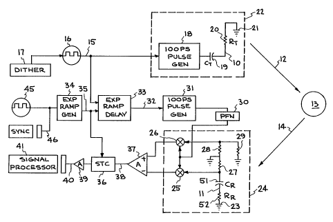
As can be seen in Fig. 1, the radar includes a one and one-quarter inch
monopole
antenna 10 for the transmitter, and a one and one-quarter inch monopole
antenna 11 for
the receiver. The transmit antenna is used to transmit a sequence of
electromagnetic
-5-
CA 02208070 1997-06-18
WO 96/19737 PCT/US95/16783
pulses. generally 12. Electromagnetic pulses echo off an object or target 13
within the
field of the sensor. The echoes, generally 14, are received by the receive
antenna 11.
The sequence of electromagnetic pulses are generated in response to a transmit
clock on line 15. The transmit clock is supplied by a pulse repetition
frequency generator 5 16, nominally at 2 megaHertz in this example. This pulse
repetition frequency generator
may be dithered using a dithering mechanism 17 if desired for noise immunity
in the =
sensor. The transmit clock on line 15 drives a 100 picosecond pulse generator
18 (e.g.
a transistor) which is coupled to the antenna 10 through a capacitor 19. The
antenna 10
is a resistively loaded monopole antenna, having a transmit load resistor 20
coupled to
a ground plane 21.
As schematically illustrated in the figure, the pulse generator 18 and antenna
10
are mounted within a waveguide cavity 22, providing shielding from other
components
on the sensor, and causing the electromagnetic pulses 12 to be issued in a
forward
direction, with limited back lobe generation.
The receive antenna 11 is coupled to a first high speed sample gate 25, and a
second high speed sample gate 26. The antenna is connected from the input of
the
sample gate 25 to ground across a resistor 27, and the input of sample gate 26
is
connected from ground across resistor 28. Also, a trim resistor RTR,M 29 is
connected
from the input of sample gate 26 to ground. Antenna 11 is a capacitively and
resistively
loaded monopole antenna, having a transmit load capacitor 51 and a series
transmit load
resistor 52 coupled to a ground plane 23. The antenna 11 and associated
components and
sample gates 25. 26 are mounted within a waveguide cavity 24.
The sample gates are strobed using a pulse forming network 30 driven by a 100
picosecond pulse generator 31 (e.g. transistor). The 100 picosecond pulse
generator is
controlled by a receive timing clock on line 32. The receive timing clock is
swept over
a range of delays by an exponential ramp delay circuit 33. The input to the
ramp delay
circuit is the transmit clock on line 15. The sweep of the ramp delay circuit
33 is
controlled by an exponential ramp generator 34 which is coupled across line 35
to the
ramp delay circuit 33. The ramp on line 35 also drives a sensitivity time
controller 36.
The sample gates 26 and 25 are coupled to differential amplifier 37. The
output
of the differential amplifier 37 is supplied on line 38 as an input to the
sensitivity time
-6-
CA 02208070 1997-06-18
WO 96/19737 PCT/US95/16783
controller. This sensitivity time controller compensates for the magnitude of
the echoes
received as the range of the echo increases.
The output of the sensitivity time controller is supplied to amplifier 39
which
supplies a range normalized equivalent time signal on line 40 representing the
echoes
being received. The sample signal on line 40 is supplied to a signal processor
41 for
indicating a characteristic of the target 13 in response to the sample signal.
The exponential ramp generator 34 is controlled by a range sweep generator 45,
nominally at 40Hertz in this example. Also, the 40Hertz range sweep generator
45 is
used to supply a sync signa146 which is used by the signal processor 41, and
otherwise
for control purposes in the network.
Thus, the pulse repetition frequency generator 16 drives a transmit pulse
generator
18 which supplies a 100 picosecond step to a resistively loaded, cavity
backed, monopole
antenna 10. The range delay path includes an exponential voltage ramp circuit
34
providing a real time range sweep circuit with, for example, a 0 to 10
nanosecond sweep
range. An equivalent time exponential ramp circuit 34 is used for reference,
such that the
two exponentials track, forming a range sweep that is very linear in time. The
exponential voltage ramp circuit is extremely simple, stable, and low cost,
providing
nanosecond speed sweep circuits. The range is swept at 40 Hertz in the
example, and the
40 Hertz sync pulse is provided to trigger a monitor scope or digitizer used
by the signal
processor 41. The delay circuit drives a fast transistor to provide a gate
pulse to the
receive sampler. The receive sampler has a transformerless differential input
with a high
common mode rejection. Differential operation is used to reduce ground
currents
coupled from the transmit pulse through the sheet inductance of the ground
plane. The
equivalent time exponential ramp also drives a sensitivity time control 36
that maintains
constant amplitude output pulses regardless of range to the target. The STC
circuit
employs FETs as attenuators that scale according to the range ramp voltage as
modified
by a range modelling circuit in the STC. A separate signal attenuator and
range
modelling attenuator FETs are forced to track with high precision through a
servo loop.
The absolute accuracy of the system is limited by drift in the gate delays and
the
= 30 components used to implement the radar. One source of such drift is the
ramp generator.
An alternative system for causing the swept delay could be based on tuned
quartz
oscillators. A first quartz oscillator used for the pulse repetition frequencv
generator is
-7-
CA 02208070 1997-06-18
WO 96/19737 PCTIUS95/16783
set at the desired frequency, such as 2 megaHertz. The second tuned quartz
oscillator
could be set at pulse repetition frequency less the sweep frequency of 40
Hertz (2
megaHertz - 40 Hertz). The second sample gate repetition frequency generator
would
drive the pulse generator in the pulse forming network to strobe the receive
sample gates.
The 40 Hertz oscillator for synchronizing the signal processor would be
triggered by
coincidence of the rising edge of the transmit pulse repetition frequency
generator, and
the receive pulse generator. Because of the stability possible for quartz
generators, the
drift in the receive and transmit timing signals could be precisely
controlled.
The dithering of the pulse repetition frequency generator provides noise
immunity
with similar systems in the same field. Thus, a number of systems could be
positioned
as desired at different spatial locations to provide imaging capabilities and
synthetic beam
forming for narrow beam applications.
Fig. 2 depicts the physical arrangement of the antennas and the differential
sampler. The transmit and receive antennas are enclosed in adjacent cavities,
the T cavity
60 and the R cavity 61. Thus, the monopole antenna 10, including the capacitor
19 and
load resistor 20 are mounted within a 1'/z inch high transmit cavity 60. Also,
the transmit
pulse generating transistor 18 is mounted within the cavity. A drive feed hole
64 is
formed in the transmit cavity 60 through which the electronics communicate.
The receive cavity 61 also includes a strobe feed hole 65 through which the
electronics are coupled to the pair of samplers 66 for the receiver. The
resistors 27 and
28 are mounted within the receive cavity. Also, the antenna consisting of the
load
resistor 52 and load capacitor 51 on the monopole 11 are mounted across the
1'/z inch
high receive cavity 61.
The transmit cavity and the receive cavity are mounted on a shielding box 70,
and
all circuitry except the items in the transmit and receive cavities are
mounted under the
shield.
The AC coupling of the resistively loaded monopole antennas 10 and 11 perform
different functions. For the transmit antenna 10, the capacitor 19 prevents
biasing on the
pulse generating transistor 18 from being shunted to ground. The capacitor 51
on the
receive antenna prevents residual low frequency currents from the transmit
pulse from
being coupled into the antenna 11 via the shield.
-8-
CA 02208070 1997-06-18
WO 96/19737 PCT/US95/16783
The transmit and receive cavities are all metal, or metal coated waveguide
cavities
with an enclosed back 71 which prevents back lobe creation by the transmit
antenna, and
improves the directional characteristic of the transmitter. With this
configuration, the
transmitted pulse will propagate with a field of view of about 1500 with less
than 3dB
attenuation relative to the main lobe. The back lobe generation will be much
smaller.
= As mentioned above, the cavities are waveguide cavities, and such are
preferably
designed with the center frequency of the pulses in mind, to operate as a
lossiess
waveguide. In the embodiment described, the approximate dimensions are 1%z
inches
high, 1'/z inches deep, and 1'/4 wide, for both the receive cavity 61 and the
transmit cavity
60. The base in the example illustrated is 3'/2 inches deep, '/z inch high,
and 3'/z inches
wide.
Note that the gate pulse generator is underneath the shielding base 70. rather
than
inside the strobe cavity, while the transmit pulse generating transistor is
mounted within
the transmit cavity.
- The sheet inductance of the radar cavities couples the transmit pulse to the
receiver, mostly through the ground plane. The differential input of the
amplifier cancels
out the ground plane noise. Also, the AC coupling on the receive antenna
limits the
amount of low frequency noise coupled into the receiver. The shielding
provided by the
transmit and receive cavities prevents direct coupling of the transmitter
pulse into the
receiver.
The waveguide launch type svstem implemented bv the waveguide cavity shown
in Fig. 2 can be improved using a horn or dielectric lens as described below
providing
gain for the receive signal and a narrow beam width.
Fig. 3 is a graph illustrating the signals generated using the radar of Fig.
2. The
plot is of the sample signal on line 40 from Fig. 1. Two traces are
illustrated, a first trace
100 showing the result of an echo at 30cm and a second trace 150 showing the
result of
an echo at 60cm. The signals include an initial pulse 101 which corresponds to
the signal
bang caused by the transmit pulse. In the trace 100, a pulse 102 is generated
from an
object at about 30cm. In trace 150, a pulse 103 is generated from an object at
about
60cm.- As can be seen, in the region between the pulse 101 and the pulse 102.
or the
pulse 101 and the pulse 103, there is verv little background noise or clutter.
The detected
-9-
CA 02208070 1997-06-18
WO 96/19737 PCT/US95/16783
echo has been measured, such that the background noise is about 30dB lower
than the
strong return echo.
The clutter in the region between the transmit bang 101 and the signal 103
comes
from a variety of sources, including ringing in the walls of the wave guide
cavities caused
by the transmit signal bang. A reduced signal to clutter ratio can be achieved
using
techniques described below with reference to Figs. 8 through 11. Further
improvements
can be achieved by suppressing clutter caused by phenomena other than antenna
cavity
ringing. In addition, digital background subtraction can be utilized, when
processing
resources are available to minimize interference form clutter. Also,
measurements
indicate that jitter of the return echo signals is very low, on the order of 1
picosecond, or
about 0.01 inches. Thus, the resolution of the sensor as configured is very
fine.
The initial pulses 101 in the traces 100 and 150 at the extreme left are
residuals
from the transmit "main bang" occurring at less than 4 inches of range.
Thereafter. slight
ripples seen in the traces going out to the echo represent ringing and clutter
that is about
30dB lower than the echoes 102 and 103 seen at 30cm and 60cm. These residuals
represent signals more than 1,000 times weaker than the transmit pulse
occurring only
a few nanoseconds earlier.
Fig. 4A illustrates two features which may be included with the radar
according
to the present invention. In Fig. 4A, the radar is represented by the symbol
200. The
radar emits a signal through a dielectric lens 201 which creates a directional
lobe 202,
improving the sensitivity and directional control of the radar.
Also, Fig. 4A illustrates use of a fiducial object 203 within the field of the
radar
200. The fiducial object may be used with or without the dielectric lens 201
as suits a
particular application. The purpose of the fiducial object is to provide
precise calibration
of the sample signal. Thus, a sample signal 204 is illustrated in Fig. 4B. It
includes the
initial bump 205, caused by the transmit pulse. An echo 206 is received from
the fiducial
object 203, and thereafter an echo 207 is received from the object 208 within
the field
202 of the radar 200. Because the fiducial object 203 is at a known position
relative to
the transmitter on the radar 200, any drift in the components of the radar
which might be
reflected in the distance between the initial pulse 205, and the echo 207 from
the object,
will be cancelled. This provides a better indication of the distance of the
object 208 from
the radar 200.
-10-
CA 02208070 1997-06-18
WO 96/19737 PCT/US95/16783
Fig. 5 illustrates yet another alternative configuration for the radar. In
particular,
Fig. 5 shows a radar 300 with an antenna horn 301 used for producing a
directional lobe
302 for the radar. As will be appreciated by those in the art, the directional
horn 301 is
another way of improving the sensitivity of the radar, and controlling the
directional
characteristics of it.
The dielectric lens of Fig. 4A, and the directional horn of Fig. 5 are
representative
of a wide variety of modifications of the antenna and cavity structure which
may be used
to control the characteristics of the field within which the sensor operates.
When using
a dielectric lens to narrow the radiation pattern and obtain antenna gain, it
is preferable
to use a low dielectric constant material such that Fabry-Perot resonances
with the
antenna cavities are reduced. For instance, a lens made of petroleum oil in a
plastic
container provides up to twenty dB gain without introducing ringing, where the
dielectric
constant e, equals 2.5 for the petroleum oil.
Fig. 6 illustrates one signal processing technique which may be used for
detecting
the distance of an object from the radar. In particular, the signal processor
in this
embodiment includes a range counter 600 which is driven by a 10 megaHertz
clock 601.
The 10 megaHertz clock 601 is enabled by gate 602. Gate 602 is turned on by
the output
of the binary element 603. The binary element is a flip-flop which is set by
the 40 Hertz
sweep generator sync signal on line 46, on each rising edge. It is reset by
output of a
comparator 604. The comparator 604 compares the sample signal from line 40
with a
threshold voltage on line 605. Also, a reset controller 606 is signalled by
the 40 Hertz
signal on line 46 to reset the range counter 600, and supplies a reset signal
on line 607
to a data processor which processes the data.
The system operates by enabling the range counter 600 at the beginning of each
sweep in response to the 40 Hertz signal on line 46. When the sample signal on
line 40
crosses the threshold, as indicated by the output of the comparator 604, the
binary
element 603 is reset, turning off the clock to the counter 600. The value of
the counter
600 is then read out, the value indicating the time between the beginning of a
range
sweep and the receiving of an echo with a sufficient magnitude.
The accuracy of the range counter 600 is determined by the drift in the timing
components, and the speed of the clock 601. With a 10 megaHertz clock, and a
40 Hertz
range sweep, the granularity of the range counter 600 is 250.000 levels per
sweep. This
-11-
CA 02208070 2005-07-20
provides highly accurate range data, which can be utilized by a signal
processing system
to indicate a variety of characteristics of the object.
Also, the 40 Hertz signal on line 46 may be replaced by a similar threshold
detector which is used to detect the initial pulse generated in the sample
signal. such as
the pulse 101, or a fiducial pulse, such as the pulse 206 using circuit
techniques known
in the art.
Figs. 7A-7G provide an electrical schematic diagram for the radar circuitry
implemented with the antenna structure shown in Fig. 2.
Fig. 7A shows the 2 megaHertz pulse repetition frequency generator which is
composed of inverter 700 in series with inverter 701. The output of inverter
700 is
connected to the input of inverter 701. A resistor 702 is connected from the
output of
inverter 700 to its input. Also, a capacitor 703 is connected from the output
of inverter
701 to the input of inverter 700.
Inverter 704 is connected from the output of inverter 700 to a charge pump
including capacitor 705 coupled to node 706. The anode of diode 707 is
connected to
node 706, and its cathode is connected to ground. The anode of diode 708 is
connected
to a-3 volt supply node 709, and its cathode is connected to node 706.
Capacitor 710 is
coupled from ground to the -3 volt supply node 709.
The pulse repetition frequency generator supplies its output on node 715. Node
715 is driven through trim resistor 716 to inverter 717. The output of
inverter 717 is
supplied to the pulse shaping circuitry described with reference to Fig. 7C
which will
ultimately drive the pulse generator.
Also, node 715 is connected through resistor 718 to node 719. Node 719 is
connected through a trim capacitor 720 to ground. Also, node 719 is the input
of inverter
721 which supplies a signal on line 722 which drives the receive timing signal
generator
circuitry of Fig. 7D.
Node 719 receives an exponential ramp through resistor 725 from the output of
op-amp 726. Op-amp 726 has its output connected to its inverting input, and
its positive
TM
input connected to node 727. Node 727 is coupled through a Mylar capacitor 728
to
ground. and to the collector of bipolar transistor 729. The collector of
transistor 729 is
also coupled through resistor 730 to a 5 volt supply. The emitter of
transistor 729 is
connected to ground. The base of transistor 729 is connected to node 731. Node
731 is
-12-
CA 02208070 2005-07-20
connected through resistor 732 to ground, and through resistor 733 and
capacitor 734 to
node 735. Node 735 is the output of a 40 Hertz scan oscillator implemented by
inverter
736 in series with inverter 737. Resistor 738 is connected from the output of
inverter 736
TM
to its input. Also, a Mylar capacitor 739 is connected from the output of
inverter 737 to
the input of inverter 736. The power supply on inverter 736 is fed by resistor
740 which
is connected to a 5 volt supply. Also, a capacitor 741 is connected from the
supplv input
of inverter 736 to ground.
Also, the output on node 735 of the 40 Hertz scan oscillator is supplied
through
resistor 745 to a sync output 746 which is used by the signal processor.
The signal on the output of op-amp 726 is an exponential ramp which is driven
through resistor 725 to the input of inverter 721.
The threshold of inverter 721 establishes an exponential delay characteristic
which balances the exponential ramp from op-amp 726 to provide a linear delay
sweep
for the signal on line 722.
The exponential ramp at the output of op-amp 726 is also connected through
resistor 750 to the inverting input of op-amp 751. Op-amp 751 has resistor 752
connected from its output to its inverting input. The positive input of op-amp
751 is
connected to ground. Also, the input of inverting op-amp 751 is connected
through
resistor 753 to a trim resistor 754 for trimming the gain of the STC. The
output of op-
amp 751 is connected on line 755 to the STC circuit of Fig. 7E.
The power supply voltages in this system as shown in Fig. 7B are supplied from
a 9 volt battery at input 756. A capacitor 757 is connected from node 756 to
ground. A
regulator 758 supplies a 5 volt output on line 759. Also, a capacitor 760 is
connected
from the output on line 759 of the regulator 758 to ground.
The signal from the output of inverter 717 of Fig. 7A is received on line 800
of
Fig. 7C. It is supplied to the input of inverter 801. Inverter 801 has its
supply input fed
by resistor 802 from a 5 volt supply. A capacitor 803 is connected from the
supply input
of inverter 801 to ground. The output of the inverter 801 is connected to the
input of
inverter 804. The output of inverter 804 is connected on line 805 to the
transmit pulse
generator shown in Fig. 7F.
Also. from Fig. 7A, the signal on line 722 is connected through capacitor 806
to
the input of inverter 807. Also, the input of inverter 807 is connected across
resistor 808
- 13 -
CA 02208070 1997-06-18
WO 96/19737 PCTIUS95/16783
to ground. The power supply input of inverter 807 is fed bv resistor 809
coupled to the
volt supply. Capacitor 810 is connected from the supply input of inverter 807
to
around. The output of inverter 807 is connected to the input of inverter 811.
The output
of inverter 811 is supplied on line 812 to the receive pulse generating
circuit in Fig. 7G.
5 Also in Fig. 7E. the signal on line 755 from op-amp 751 is received through
an
STC model circuit composed of resistor 820 in parallel with the series
connection of
resistor 821 and diode 822. This circuitry provides a model of the sensitivity
time
characteristic to be compensated for by the STC circuit to provide increasing
gain with
increasing range. The output of the STC model is connected to node 823. Node
823 is
connected to the positive input of op-amp 824. The inverting input is
connected to node
825. Node 825 is connected through resistor 826 to the 5 volt supply, and
through
capacitor 827 to the output of the op-amp 824. Also, a resistor 899 is
connected from
node 825 to ground. The output of op-amp 824 is also connected to the gate of
FET
transistor 830. The drain of FET transistor 830 is connected to node 823. The
source of
FET transistor 830 is connected to ground. Similarly, the output of the op-amp
824 is
connected to the gate of FET 831. The drain of FET 831 is connected to node
832. The
source of FET 831 is connected to ground. The FET 831 provides controlled
attenuation
of the signal at the node 832 for the STC compensation.
The output of the differential amplifier in the receiver is received on line
840 from
the circuitry of Fig. 7G. It is supplied through capacitor 841 to node 842.
Node 842 is
connected through resistor 843 to ground. and through resistor 844 to node
832. Node
832 is connected to the positive input of op-amp 845. The inverting input of
op-amp 845
is connected through resistor 846 in series with capacitor 847 to ground.
Also, a resistor
848 is connected from the output of op-amp 845 to its inverting input. The
output of the
op-amp 845 is supplied through a resistor 849 to a video output 850. Capacitor
851 is
also coupled between the video output 850 and ground. The video output 850
provides
the equivalent time sample signal as described above.
Figs. 7F and 7G illustrate the balance of the circuitry in the radar. The
transmit
timing clock on line 805 is coupled through a capacitor 900 to node 901. Node
901 is
connected through resistor 902 to ground and through resistor 903 to the base
of
transistor 904. The emitter of transistor 904 is connected to ground. The
collector of
transistor 904 is connected through resistor 905 to node 906. Node 906 is
connected
-14-
_
CA 02208070 1997-06-18
WO 96/19737 PCT/US95/16783
through a capacitor 907 to ground and through a resistor 908 to node 910. Node
910 is
connected through capacitor 911 to ground, and through resistor 912 to the 5
volt supply.
Also, the collector of transistor 904 is AC coupled through capacitor 920 to
the monopole
antenna 921 which is resistively loaded by resistor 922. The resistively
loaded monopole
antenna is about 1'/4 inches long in this embodiment. Also, the dashed lines
923 illustrate
the components which are mounted within the transmit cavity.
The receive timing signal is received on line 812, and coupled through
capacitor
930 to node 931. Node 931 is connected across resistor 932 to ground and
through
resistor 933 to the base of high speed bipolar transistor 934. The emitter of
transistor 934
is connected to ground. The collector of transistor 934 is connected through
resistor 935
to node 936. Node 936 is connected across resistor 937 to the 5 volt supply,
and across
capacitor 938 to ground. The collector of transistor 934 also supplies the
gate pulse
through capacitor 939 to strobe the sampling gates in the receive cavity. The
receive
cavity is outlined generally by dotted line 940.
A number of components are mounted within the receive cavity 940, including
the resistively loaded monopole antenna, capacitor 945, antenna 946, and
resistor 947.
The antenna is connected from node 948 through resistor 949 to ground, and
through a
capacitor 950 to the anode of sampling diode 951. A cathode of diode 951 is
connected
to receive the receive strobe pulse from line 952 through the capacitor 939.
Also, line
952 is connected through a resistor 953 to ground. The anode of diode 951 is
connected
through resistor 954 to node 955. Node 955 is connected across resistor 956 to
the
positive input of op-amp 957. Also, the positive input of op-amp 957 is
connected across
resistor 958 to ground. The negative power supply on op-amp 957 is coupled to
the -3
volt supply (from Fig. 7A), and across capacitor 960 to ground. The output of
op-amp
957 is connected to the inverting input, and through capacitor 961 and
resistor 962 to the
inverting input of op-amp 963. The inverting input of op-amp 963 is coupled
through
resistor 964 to its output. The positive power supply on the op-amp 963 is
coupled to the
5 volt supply.
The positive input of op-amp 763 is driven through a second sample gate which
is connected as follows. In particular, a sampling diode 970 has its cathode
connected
to line 952 to receive the gate pulse. The anode of diode 970 is connected
through
-15-
CA 02208070 2005-07-20
capacitor 971 to node 972. Node 972 is connected through resistor 973 to
ground. Also.
a trim resistor 974 may be included between node 972 and ground.
The anode of diode 970 is connected through resistor 980 and resistor 982 to
the
positive input of the op-amp 963. The node between resistor 980 and resistor
982 is
connected through capacitor 983 to ground. There is a similar capacitor 984
connected
between node 955 and ground. Resistor 985 is connected from the positive input
of the
op-amp 963 to ground.
In Figs. 7A-7G, inverters 700, 701, 704, 717, 721, 736 and 737 may be
implemented with 74HC04. The inverters 801, 804, 807 and 811 may be
implemented
with 74AC04. The op-amps 726, 751, 824, 845, 963, and 957 may be implemented
using
the component TLC272. The regulator 758 is implemented with a 812-50
manufactured
by Seiko. The transistors 830 and 831 are on a CD4007, with pin 14 at 5 volts
and pin
7 at ground. All the diodes are implemented with IN4148's unless noted in the
figure.
Transistors 904 and 934 are implemented using NE68533. Transistor 729 is
implemented using a 2N2222. Component values listed in the figure are
representative
of one implementation. They may be adjusted to suit the needs of a particular
application.
This circuitry provides a differential sampling structure with very high
common
mode rejection as discussed above. Alternative implementations of the
differential
receiver circuitry are described in United States Patent 5,345,471 issued
September 6,
1994, entitled Ultra-Wide Band Receiver.
Figs. 8, 9. 10, and 11 A through 11. C illustrate techniques for reducing
clutter, by
damping ringing in the transmit and receive cavities. Fig. 8 illustrates the
use of the
double wall structure between the cavities. Thus. a transmit cavity 1000 and a
receive
cavity 1001 are mounted on an electronics cavity 1002. A printed circuit board
1003
buffers the electronics cavity 1002 from the transmit cavity and receive
cavity 1001.
Within the transmit cavity, a leaf antenna 1004 is coupled to a transmit pulse
drive
transistor 1005, and to a series connection of resistor Rt (about 220 ohms)
and capacitor
Ct (about 2 picoFarads). This configuration makes a resistively loaded
monopole
antenna for transmitting the transmit pulse into the field. The transmit
cavity 1000 is
-16-
CA 02208070 1997-06-18
WO 96/19737 PCT/US95/16783
configured in a wave guide configuration having height of about 1.5 inches and
a width
of about 1.5 inches. The transmit cavity has back wall 1006, a side wall 1007,
a top wall
1008. and a bottom wall 1009. An interior wall 1010 encloses the cavity. The
walls of
the transmit cavity are made using brass in this embodiment.
The receive cavity similarly includes a leaf antenna 1015 mounted in a
resistively
coupled monopole configuration using a resistor Rt (about 220 ohms) and
capacitor Ct
(about 2 picoFarads) in series to connect it to the receive cavity 1001. The
sampling
electronics 1016 are located at a feed point and inside the electronics cavity
1002. The
receive cavity, also made of brass in this example. has a top wall 1017, a
side wall 1018,
a bottom wall 1019. and a back wall 1020. An interior wall 1021 encloses the
cavity.
The dimensions of the receive cavity are substantially the same as those of
the transmit
cavity. As shown in Fig. 8, the combination of the receive cavity 1001 and
transmit
cavity 1000 form a double wall structure by spacing apart the interior walls
1010 and
1021 of the respective cavities. The region 1022 between the walls 1010 and
1021 may
be filled with air, or another dielectric material, such as a printed circuit
board or the like.
This prevents the signal bang caused by the transmit pulse from being directly
coupled
into the receive cavity walls from the transmit cavitv, substantially reducing
ringing and
signal clutter. The top and bottom walls of the transmit and receive cavities
may be
metallically contiguous.
Fig. 9 illustrates another technique for reducing ringing based on a
conductive
damping element in the transmit and receive cavities. The transmit and receive
cavities
are configured in Fig. 9 just as they are in Fig. 8. The elements of these
cavities are not
redescribed herein. The additional feature shown in Fig. 9 is made up of the
conductive
damping elements 1030, 1031, 1032, and 1033. These damping elements each
consist
of a conductive element which is connected at two places to the perimeter of
the opening
of the cavities. Thus, the conductive damping element 1031 is connected to the
corner
1035 of the transmit cavity, and to one side of the perimeter of the opening
in the transmit
cavity, substantially near the center, such as at point 1036. The conductive
damping
elements include a resistor Rd which is about 100 ohms in this example. These
resistive
damping elements are preferably placed along the side walls of the cavity, and
flush with
the opening or extending out into the field slightly. These narrow band
dampers
eliminate long lasting, high Q ringing which results from the transmit bang
signal. The
-17-
CA 02208070 1997-06-18
WO 96/19737 PCT/US95/16783
triangular shape is not critical, but appears to be preferred based upon trial
and error (the
conductors could be, for instance, formed in a rectangular shape). The
orientation plane
in which these triangle sections lie is also not critical. The total length of
the conductor
is shown to approximate scale in the figure. There appears to be a narrow band
impedance transformation along the length of the conductor that aids in
ringing
suppression, so that conductor length needs to be approximately as shown. The
length
of the conductors and the resistance can be empirically determined based on a
particular
implementation and design of the transmit and receive cavities used.
Fig. 10 illustrates another technique for reducing clutter in the received
signal.
The transmit and receive cavities are configured substantiallv as shown in
Fig. 8 and are
not redescribed here. The feature illustrated in Fig. 10 is narrow band
radiative damping
elements 1040 and 1041. These elements comprise damping resistances of Rn of
about
100 ohms, and radiative conductors which extend approximately an inch out from
the
center of the opening of the transmit cavity and receive cavity on the
interior walls 1010
and 1019. Again, the length and resistances can be empirically determined
based on the
particular design of the transmit and receive cavities.
Fig. 11 A illustrates yet another alternative for reducing clutter. According
to the
alternative shown in Fig. 1 lA, triangular terminating plates are coupled to
the perimeter
of the opening of the transmit and receive cavities 1000 and 1001. Again, the
transmit
and receive cavities are configured as shown in Fig. 8 and are not redescribed
here. The
triangular plates include plate 1050 which is coupled to the perimeter of the
opening of
the transmit cavity 1000 along the top wall of the cavity. Triangular plate
1051 is
coupled to the perimeter of the opening of the receive cavity 1001 along the
top wall.
Triangular element 1052 is coupled to the perimeter of the opening of the
transmit cavity
1000 along the bottom wall, triangular element 1053 is coupled to the
perimeter of the
opening of the receive cavity 1001 along the bottom wall. Triangular element
1054 is
coupled to the perimeter of the opening of the transmit cavity 1000 along the
outside
wall. Triangular element 1055 is coupled to the perimeter of the receive
cavity 1001
along the outside wall. The plane in which the triangular elements 1054 and
1055 lie
substantially parallel to the plane of the openings 1057 and 1058. The
terminating
elements 1050, 1051. 1052, and 1053 are folded slightly toward the field being
sensed,
such as at a 45 angle. This supplies some antenna gain, damps residual
ringing, and
-18-
CA 02208070 1997-06-18
WO 96/19737 PCT/US95/16783
provides some side load suppression. Again, the dimensions of these plates are
substantially as illustrated in the figure, using triangular elements which
are equilateral
triangles having a peak of about one inch away from the plane of the openings
in the
transmit and receive cavities.
Fig. 11B illustrates how the triangular elements 1050, 1051, 1052, and 1053
are
folded into the field being sensed at an angles of about 45 . The triangular
element 1055,
however, lies substantially in the plane of the opening. Fig. 11 C illustrates
the
configuration of the triangular elements 1055 and 1054. Thus, the transmit
cavity 1000
and receive cavity 1001 are shown in top view. The triangular elements 1050
and 1051
can be seen leaning into the field being sensed. The triangular elements 1055
and 1054
extend substantially at right angles away from the side walls of the transmit
and receive
cavities. However, it may be desirable to flatten the triangular elements
1050, 1051,
1052, and 1053 so that the mechanism can be smoothly dragged along a surface
without
hanging on the triangular terminating plates.
The microradar rangefinder embodiments of Figures 2, 8-11 A all have a side-by-
side radiator configuration as generally shown in Figure 12. Each such ultra-
wideband
radar rangefinder has a transmit cavity 1100 and a receive cavity 1102
arranged side-by-
side with vertical internal radiator elements 1104, 1106 that are spaced apart
and parallel.
(The radiator elements include both a transmit radiator element 1104 and a
receive
radiator element 1106). These radiator elements 1104, 1106 can be wires or
metal strips
of about 1/4" width for a 2GHz center frequency system, and they are
terminated at their
far ends with resistors, typically RTI = RT, = 2000.
A primary problem with this side-by-side arrangement is that the E-fields 1108
from each cavity terminate on adjacent sides of a metal septum or dividing
wall 1110.
The septum 1110 is X/4 long, or.X/8 long from either end to the center. Thus,
the septum
1110 is isolated from the grounded end regions by X/8, thereby exhibiting a
non-zero
impedance to the E-fields 1108. As a consequence, coupling occurs between the
cavities
1100, 1102 that results in a substantial "main bang" pulse which obscures
reflections
from nearbv objects, e.g., from 0 to 6". In the embodiments of Figures 8-11A,
the
septum 1110 comprises two closely spaced metal plates, rather than one plate
as shown,
to help reduce this coupling.
-19-
CA 02208070 1997-06-18
WO 96/19737 PCT/US95/16783
A secondarv limitation to this side-by-side configuration is the difficulty in
assemblv of the metal cavities 1100, 1102 about the PCB 1112, which separates
the
cavities 1100, 1102 from shielded electronics cavity 1114.
Figure 13 shows an alternate antenna configuration where the E-fields do not
terminate on adjacent sides of a septum. Rather, they are far apart.
Additionally, the far
ends of the radiators, with termination resistors RT,, Rr, are at maximum
distance for best
T-R isolation. The UWB radar rangefinder comprises a transmit cavity 1120 and
a
receive cavity 1122, which are separated by an air gap 1121. The radiator
elements 1124,
1126 extend in opposed directions from near air gap 1121. The radiator
elements are
wires or metal strips which are generally coplanar but extend in opposed
directions. The
E-fields 1128, which extend from radiators 1124, 1126 thus do not terminate at
a
common plane between cavities 1120, 1122. Experiments show this configuration
to be
nearly lOx better than the side-by-side configuration regarding main bang
coupling.
Further, the horns (i.e., cavities 1120, 1122) need not be in metallic
contact, i.e.. they can
be separated by air gap 1121, and can be snapped onto the PCB using finger
stock to
retain them.
Figures 14A and 14B provide a front and side view of the transmit and receive
cavities 1130, 1132 to better illustrate the placement of the horns 1130, 1132
and their
internal radiators 1134, 1136. As in side-by-side embodiments, the radiator
may be a
wire, or it may be a metal strip of some experimentally determined width that
optimized
radiation efficiency and bandwidth. Horns 1130, 1132 are separated by an air
gap 1131
and are mounted on a PCB 1138 which separates horns 1130, 1132 from
electronics
cavity (shield) 1140 which contains the various rangefinder electronic
components 1142,
mounted on the reverse side of PCB 1138.
Transmit radiator (e.g., wire) 1134 extends from transmitter output T on PCB
1138 to a distal wall of horn 1130 through termination resistor RT,.
Similarly, receive
radiator (e.g., wire) 1136 extends from receiver input R to a distal wall of
horn 1132
through termination resistor RT2. Transmitter output T and receive input R are
located
inside horns 1130, 1132 near the air gap 1131 separating the horns 1130, 1132.
Thus.
radiators 1134, 1136 extend away from the interface between the two cavitites
1130,
1132. Cavity 1130 transmits a pulse towards an object, and cavity 1132
receives an echo
reflected back from the object.
-20-
CA 02208070 1997-06-18
WO 96/19737 PCT/US95/16783
Figure 14C depicts a more complex radiator configuration, a top-loaded
radiator
wherein the drive/pickoff is connected to the top, or high impedance end, of a
monopole
that is approximately 1/4 long at the radar's center frequency. Transmit
cavity/horn 1150
contains a transmit radiator 1152 which is formed of two sections 1154, 1156
which are
connected through a bend or hairpin turn 1158. Similarly receive cavity/horn
1160
contains a receive radiator 1162 which is formed of two sections 1164, 1166
which are
connected through a bend or hairpin turn 1168 . The horns 1150, 1160 are
mounted on
a PCB 1170 which has a shield or cavity 1172 mounted on the reverse side.
Radiators
1152, 1162 thus extend from output T, input R across the cavity and back,
terminating
at the distal walls in RTI, R. With this connection, both the transmit antenna
and the
receive antenna provide about 6dB gain over that of Figure 14B, which is
similar to the
embodiments of Figure 12. It is thought that radiation from sections 1154,
1156 are
additive when the distance between the centers of section 1154, 1156 are
separated by X/4
along the wire's hairpin turn 1158.
As a final improvement, the receive radiator 1162 is left unterminated on the
PCB
1170, at the receiver R input. This results in a doubling of the received
voltage and thus
an improvement in sensitivity. Far end termination resistors RTI, R-I-, reduce
or eliminate
ringing. In all, this configuration provides about 18dB more sensitivity over
the
configuration of Figure 12.
Thus the opposed radiator arrangement shown generally in Figure 13, and
illustrated more specifically in Figures 14A-C, significantly reduces main
bang coupling
between the cavities over the side-by-side configuration shown generally in
Figure 12
and illustrated more specifically in Figures 2, 8-11 A. In addition, the
conductive
damping elements shown in Figures 8-1 lA for the side-by-side arrangement are
not
generally required in the opposed radiator arrangement.
With the alternate antenna configuration of the opposed arrangement, main bang
coupling from the transmit antenna to the receive antenna are reduced so that
the radar
can operate at zero range, thus allowing the detection of near-surface objects
such as the
human heart or rebar in concrete. Uses include heart monitoring, wall
thickness
measurements, bridge deck imaging and radar altimeters. The lower cost and
simplified
assembly also provided by the opposed antenna configuration allow high volume
applications such as non-contact gas tank fill-level measurements.
-21 -
CA 02208070 1997-06-18
WO 96/19737 PCTIUS95/16783
Accordingly, a highly accurate, low cost. simple to implement wide band radar
sensor is provided with a swept range gate which provides an amplitude versus
time
sample signal making the radar useful as a radar range finder. The radar range
finder of
the present invention replaces ultrasound ranging sensors used in industry
which suffer
the variation in speed of sound over temperature and humidity, reflections off
foam in
vats giving false level measurements and the like, industrial environments
generating
ultrasonic interference, and the inability of ultrasound to penetrate panels.
or a dirt or
water overcoating blocking the transducer. All of these deficiencies are
solved by the
present invention, with a low cost, versatile, and highly accurate sensor.
Besides the fluid level measurement systems which have been primarily
implemented with ultrasound in the prior art, the present invention has other
immediate
uses in automotive parking assistance and cruise control radar. Yet another
use for this
sensor is hidden object location, such as finding and precisely ranging
between wall studs
and pipes, rebar in concrete, weapons in briefcases or mattresses, and buried
wires and
pipes. The range finding applications also have many uses in the robotics
field.
Although the embodiment described is based on a transmitter which issues a
sequence of single impulse RF signals by the transmitter, a similar system can
be
implemented using a sequence of bursts of RF energy of several cycles in
length. The
impulse transmission embodiment may have limited applications because of
Federal
Communications Commission Part 15 regulations over the transmission methods
allowed
for wide band pulses.
Another application of the present invention is an educational one. In
particular,
time domain electromagnetics can be studied using this simple radar with an
equivalent
time output signal. A student may, in real time, monitor the characteristics
of the field
of the radar in a manner to be studied, and watch the results on the echoed
pulses in the
sample signal.
Thus, the present invention has provided a low cost, high accuracy radar with
high
resolution swept range gate for close range applications. The uses include
automotive
parking assistance, curb sensing, active suspension system sensing, occupant
position
sensing, and other applications where the precise range of an object needs to
be
determined. The range finder also makes an excellent fluids and solids level
sensor for
petroleum storage tanks, industrial mixing vats, and grain silos. Its
amplitude scan
-22-
CA 02208070 2005-07-20
displav also indicates the presence or absence of objects behind barriers,
such as studs
behind walls and rebar in concrete. The device can also be used in medical
applications
to sense movement of organs such as the heart within the swept range.
The foregoing description of a preferred embodiment of the invention has been
presented for purposes of illustration and description. It is not intended to
be exhaustive
or to limit the invention to the precise forms disclosed. Obviously, many
modifications
and variations will be apparent to practitioners skilled in this art. It is
intended that the
scope of the invention be defined by the following claims and their
equivalents.
-23-