Note: Descriptions are shown in the official language in which they were submitted.
i CA 02208276 1997-06-09
A
' -1-
TITLE OF THE INVENTION
MULTIBAND MOBILE UNIT COMMUNICATION APPARATUS
BACKGROUND OF THE INVENTION
Z. Field of the Invention
This invention relates to a mobile unit
communication apparatus for communicating with at least a
mobile unit system.
2. Description of the Prior Art
A mobile unit communication apparatus for receiving
a radio wave signal transmitted from a mobile unit system
is known. Japanese patent application provisional
publication No. 6-132849 discloses such a mobile unit
communication apparatus. In this prior art mobile unit
communication apparatus, a smaller number of local
oscillators are used. To provide transmission and
reception through different frequencies respectively, a
local oscillator capable of directly or indirectly
oscillating a fundamental wave and its multiple wave is
used, and a local oscillator is used for transmission and
reception commonly.
SUMMARY OF THE INVENTION
The aim of the present invention is to provide an
improved mobile unit communication apparatus.
According to the present invention, a multiband
mobile unit communication apparatus is provided, which
CA 02208276 1997-06-09
-2-
comprises: an antenna portion for receiving a plurality of
radio wave signals respectively transmitted from a
plurality of mobile unit communication systems, the
plurality of radio wave signals having different carrier
frequencies respectively; a plurality of independent
circuits for generating a plurality of intermediate
frequency signals from the plurality of radio wave signals
from the antenna portion respectively; and a common circuit
including a receiving portion for receiving one of the
plurality of intermediate frequency signals in accordance
with a mode signal, a quadrature demodulation circuit for
directly converting one of the plurality of intermediate
frequency signals into I and Q baseband signals, and a
decoding circuit for outputting a decoding result from the
I and Q baseband signals.
In the multiband mobile unit communication apparatus,
the receiving portion may comprise a power supply control
portion for supplying a power to one of the independent
circuits in accordance with the mode signal.
In the multiband mobile unit communication apparatus,
the receiving portion may comprise a switch for supplying
one of the plurality of intermediate frequency signals to
the receiving portion in accordance with the mode signal.
In the multiband mobile unit communication apparatus,
the common circuit may further comprise a switchable
k
CA 02208276 1997-06-09
' -3-
frequency dividing circuit for selectively
frequency-dividing the second local oscillation signal in
response to the mode signal such that the frequency-divided
signal having frequencies corresponding to frequencies of
the plurality of intermediate frequency signals, the
frequency-divided signal being supplied to the quadrature
demodulation circuit.
In the multiband mobile unit communication apparatus,
the antenna portion may comprise first and second antennas,
a switch for selectively supplying outputs of the first and
second antennas to one of the plurality of independent
circuits, and the multiband mobile unit communication
portion may further comprise: a receiving level estimating
portion for estimating a level of one of the radio wave
signal from the converted I and Q baseband signals and an
antenna switching control portion for controlling the
switch in accordance with the level to provide a antenna
diversity receiving.
In the multiband mobile unit communication apparatus,
each of the plurality of independent circuits may comprise:
a first bandpass filter for bandpass-filtering each of the
plurality of radio wave signals from the antenna portion;
an amplifier for amplifying an output of the first bandpass
filter; a filter portion for filtering an output of the
amplifier; a mixer for mixing an output of the filtering
4
CA 02208276 1997-06-09
_4_
portion with a first local oscillation signal to generate
an intermediate frequency signal; a second bandpass filter
for bandpass-filtering the intermediate frequency signal
and the common circuit may further comprise: a variable
gain amplifying portion for amplifying one of the plurality
of intermediate frequency signal with a gain thereof
controlled in accordance with a gain control signal and
supplying the amplified intermediate frequency signal to
the quadrature demodulation circuit; a first a/d converter
for a/d converting the I baseband signal and supplying the
converted I baseband signal to the decoding circuit; a
second a/d converter for a/d converting the Q baseband
signal and supplying the converted Q baseband signal to the
decoding circuit; a level detection portion for detecting
levels of the converted I and Q baseband signals; a gain
control signal generation portion for generating the gain
control signal in accordance with the detected level; a
mode signal generation portion for generating the mode
signal; a first local oscillation signal generator for
generating the first local oscillation signal; and a second
local oscillation signal generator for generating the
second local oscillation signal.
In this case, the filtering portion may comprise a
bandpass filter.
Moreover, in this case, the filtering portion may
CA 02208276 1997-06-09
s
-5-
comprise a high-pass type of matching circuit.
Moreover, in this case, the mode signal generator
generates the mode signal in accordance with an operational
condition and a communication condition of the multiband
mobile unit communication apparatus.
Moreover, in this case, the variable gain amplifying
portion may comprise an analog gain control signal input
and the gain control signal generation portion may further
comprise a d/a converter and the gain control signal
generation portion generates data from the detected level
and the d/a-converts the data to supply the gain control
signal to the analog gain control signal input.
Moreover, in this case, the variable gain control
portion may comprise a digital gain control signal input
and the gain control signal generation portion generates
the gain control signal of digital data from the detected
level and supplies the gain control signal to the digital
gain control signal input.
Moreover, in this case, the variable gain amplifying
portion may comprise a plurality of amplifiers in series, a
switchable tuning circuit having a plurality of tuning
circuits having tuning frequencies corresponding to the
plurality of intermediate frequencies respectively, and a
switching portion for selecting one of the plurality of
tuning circuits in accordance with the mode signal.
c
CA 02208276 1997-06-09
' -6-
Moreover, in this case, the common circuit may
further comprise a f_Crst switchable low-pass filter for
low-pass-filtering the I baseband signal with a first
cutoff frequency controlled in accordance with the mode
signal such that the first cutoff corresponds to a
transmission rate of the I baseband signal and a second
switchable low-pass filter for low-pass-filtering the Q
baseband signal with a second cutoff frequency controlled
in accordance with the mode signal such that the second
cutoff corresponds to a transmission rate of the Q baseband
signal.
Moreover, in this case, the common circuit may
further comprise a high isolation amplifier for amplifying
an output of the switch with a relatively high isolation
characteristic.
BRIEF DESCRIPTION OF THE DRAWINGS
The object and features of the present invention
will become more readily apparent from the following
a_~_s,_a a_ -__~~_ _,___ ,_
uc~ixlleu uesCry~l~u tatcen in conjunction Wlth Lhe
accompanying drawings in which:
Fig. 1 is a block diagram of a multiband mobile unit
communication apparatus of a first embodiment;
Fig. 2 is a block diagram of a multiband mobile unit
communication apparatus of a second embodiment;
Fig. 3 is a block diagram of a multiband mobile unit
CA 02208276 1997-06-09
x
r
_7_
communication apparatus of a third embodiment;
Fig. 4 is a block diagram of a multiband mobile unit
communication apparatus of a fourth embodiment;
Fig. 5 is a schematic circuit diagram of the fourth
embodiment showing the switchable tuning circuit and the
variable gain amplifier in Fig. 4;
Fig. 6 is a block diagram of a multiband mobile unit
communication apparatus of a fifth embodiment;
Fig. 7 is a block diagram of a multiband mobile unit
communication apparatus of a sixth embodiment;
Fig. 8A is a block diagram of a multiband mobile
unit communication apparatus of a seventh embodiment;
Fig. 8B is a block diagram of the seventh embodiment
showing the high-pass type of matching circuits 111 and 112;
Fig. 8C is a graphical drawing of the seventh
embodiment;
Fig. 9 is a block diagram of a multiband mobile unit
communication apparatus of an eighth embodiment; and
Fig. 10 is a block diagram of a multiband mobile
unit communication apparatus of a ninth embodiment.
The same or corresponding elements or parts are
designated with like references throughout the drawings.
DETAILED DESCRIPTION OF THE INVENTION
<FIRST EMBODIMENT>
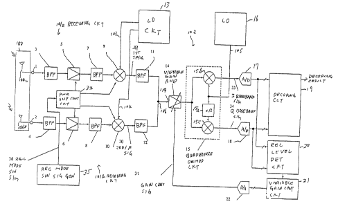
Fig. 1 is a block diagram of a multiband mobile unit
CA 02208276 1997-06-09
1
communication apparatus of a first embodiment.
The multiband mobile unit communication apparatus of
the first embodiment comprises an antenna portion 100 for
receiving first and second radio wave signals transmitted
from first and second mobile unit communication systems,
said first and second radio wave signals having first and
second carrier frequencies respectively, first and second
receiving circuits (independent circuits) 101a and lOlb, as
independent circuits, for generating first and second
intermediate frequency signals from said first and second
radio wave signals from the antenna portion 100 in first
and second modes, respectively; and a common circuit 102
for directly converting the first intermediate frequency
signal 29 into first I and Q baseband signals in said first
mode and directly converting said second intermediate
frequency signal 30 into second I and Q baseband signals in
said second mode, for decoding from the I and Q baseband
signals in the first and second modes, and for generating
the mode signal. The common circuit 102 has an input 106
for receiving either of the first or second intermediate
frequency signal from the bandpass filter 11 or 12.
The antenna portion 100 comprises first and second
antenna 100a and 100b for receiving first and second radio
wave signals respectively. The antenna may comprise a
single antenna for receiving first and second radio wave
CA 02208276 1997-06-09
signals and a separator (not shown) for separating the
first and second radio wave signals and distributing the
received first and second radio wave signals to the
bandpass filters 3 and 4 respectively.
The first and second receiving circuits lOla and
lOlb are independently used for receiving the first and
second radio wave signals transmitted from first and second
mobile unit communication systems. On the other hand, the
common circuit 102 is commonly used for processing the
first and second radio wave signals.
The first receiving circuit lOla comprises a
bandpass filter 3 for bandpass-filtering the first radio
wave signal from the antenna 100a to suppress unnecessary
components, an amplifier 5 for amplifying an output of the
bandpass filter 3, a bandpass filter 7 for
bandpass-filtering an output of the amplifier 5 to suppress
unnecessary components, a mixer 9 for mixing an output of
the bandpass filter 7 with a first oscillation signal 103
to generate a first intermediate frequency signal 29, a
bandpass filter 11 for bandpass-filtering the first
intermediate frequency signal 29.
Similarly, the second receiving circuit 101b
comprises a bandpass filter 4 for bandpass-filtering the
second radio wave signal from the antenna 100b to suppress
unnecessary components, an amplifier 6 for amplifying an
CA 02208276 1997-06-09
~ -10-
output of the bandpass filter 4, a bandpass filter 8 for
bandpass-filtering an output of the amplifier 6 to suppress
unnecessary components, a mixer 10 for mixing an output of
the bandpass filter 8 with a second oscillation signal 104
to generate a second intermediate frequency signal 30, a
bandpass filter 12 for bandpass-filtering the second
intermediate frequency signal.
A local oscillation circuit 13 generates first and
second local oscillation signals.
ZO The common 102 comprises a variable gain amplifier
14 for respectively amplifying the first and second
intermediate frequency signals 29 and 30 in first and
second modes with gains controlled, a quadrature
demodulation circuit 15 for directly converting an output
signal from the variable gain amplifier 14 into I and Q
baseband signals into I and Q baseband signals 33 and 34
using a third local oscillation signal 105, an a/d
converter 17 for converting the I baseband signal 33 into a
digital I baseband signal, an a/d converter 18 for
converting the Q baseband signal 33 into a digital Q
baseband signal, a decoding circuit 19 for decoding the
digital I and Q baseband signals to output a decoding
result, a receiving level detection circuit 20 for
detecting levels of the digital I and Q baseband signals, a
variable gain amplifier control circuit 21 for generating
CA 02208276 1997-06-09
-11-
gain control data in accordance with the detected levels
from the receiving level detection circuit 20, a d/a
converter 22 for converting the gain control data to
generate a gain control signal 31. The gain of the
variable gain amplifier 14 is controlled in accordance with
the gain control signal 31.
The quadrature demodulation circuit 15 comprises a
phase shifter 15a for phase-shifting the third local
oscillation signal by 1/2 n and mixers 15b and 15c for
mixing the output of the variable gain amplifier 14 with
the third local oscillation signal and 1/2 ~ -phase shifted
local oscillation signal.
The common circuit 102 of the multiband mobile unit
communication apparatus further comprises a receiving mode
switching signal generation circuit 35 for generating a
receiving mode switching signal 36 and a supply power
control circuit 32 for supplying a supply power to the
amplifier 5 and the mixer 9 in the first mode and the
supply power to the amplifier 6 and the mixer 10 in the
second mode.
An operation of the multiband mobile unit
communication apparatus of the first embodiment will be
described.
The antenna portion 100 receives first and second
radio wave signals having different frequency bands
CA 02208276 1997-06-09
-12-
transmitted from different mobile unit base stations.
In this multiband mobile unit communication
apparatus, the radio wave frequency band is selected in
accordance with the receiving mode switching signal 36. In
response to this receiving mode switching signal 36, the
power supply control circuit 32 supplies the power to the
receiving circuit selected and stops supplying the power to
the receiving circuit not selected.
The bandpass filter 3 suppresses unnecessary
components other than the first radio wave signal in the
received radio signal components from the antenna portion
100. The amplifier 5 amplifies the output of the bandpass
filter 3. The bandpass filter 7 suppresses unnecessary
components other than the first radio wave signal in the
output of the amplifier 5, particularly suppresses an image
frequency with respect to the local oscillation signal 103
and the first radio wave signal inputted into the amplifier
5. The mixer 9 mixes the output of the bandpass filter 7
with the first oscillation signal to generate the first
intermediate frequency signal 29. The local oscillation
signal generation circuit 13 generates the first and second
local oscillation signals.
The bandpass filter 11 performs bandpass-filtering
to suppress unnecessary components generated by the mixing
in the mixer 9 to selectively output the first intermediate
CA 02208276 1997-06-09
' -13-
frequency signal.
The variable gain amplifier 14 amplifies the first
intermediate frequency signal 29 in the first mode with its
gain controlled in accordance with the gain control signal
31. The quadrature demodulation circuit 15 directly
converts the output signal from the variable gain amplifier
14 into I and Q baseband signals 33 and 34 using the third
local oscillation signal 105.
The local oscillator 16 supplies the third local
oscillation signal 105 having a local oscillation frequency
determined by the intermediate frequencies of the first and
second intermediate frequency signals 29 and 30.
The a/d converters 17 and 18 convert the I baseband
signal 33 and Q baseband signal 34 into the digital I
baseband signal and the digital Q baseband signal.
The decoding circuit 19 decodes the digital I and Q
baseband signals to output the decoding result. The
receiving level detection circuit 20 detects levels of the
digital I and Q baseband signals. The variable gain
amplifier control circuit 21 generates the gain control
data in accordance with the detected levels from the
receiving level detection circuit 20. The d/a converter 22
converts the gain control data into the gain control signal
31. The gain of the variable gain amplifier 14 is
controlled in accordance with the gain control signal 31.
CA 02208276 1997-06-09
4
-14-
The receiving mode switching signal generation
circuit 35 generates the receiving mode switching signal 36
in accordance with the condition of the mobile unit
communication apparatus, that is, an operation to an
operation panel (not shown) and a call from either of the
first and second mobile unit communication systems. The
supply power control circuit 32 supplies the power to the
amplifier 5 and the mixer 9 in the first mode and to the
amplifier 6 and the mixer 10 in the second made to
selectively supplying the first or the second intermediate
frequency signal to the variable gain amplifier, to save a
power consumption, to suppress noises and to selectively
supply the intermediate frequency signal to the variable
gain amplifier 14.
In the second mode, the receiving circuit 101b
receives the second radio wave signal and supplies the
second intermediate frequency signal to the variable gain
amplifier 14. During this, the power is supplied to the
amplifier 6 and the mixer 10, and the common circuit 102
outputs the decode result by the decoding circuit 19 from
the second radio wave signal as similar to the first mode.
The variable gain amplifier 14 respectively
amplifies the first and second intermediate frequency
signals 29 and 30 via an analog input 114 in the first and
second modes with gains controlled in accordance with the
CA 02208276 1997-06-09
-15-
gain control signal 31 from the variable gain control
circuit 21 via the d/a converter 22. The quadrature
demodulation circuit 15 directly converts the output signal
from the variable gain amplifier 14 into I and Q baseband
signals 33 and 34 using the third local oscillation signal
105. The a/d converter 17 converts the I baseband signal
33 into a digital I baseband signal. The a/d converter 18
converts the Q baseband signal 33 into a digital Q baseband
signal. The decoding circuit 19 decodes the digital I and
Q baseband signals to output the decoding result.
The receiving level detection circuit 20 detects the
levels of the digital I and Q baseband signals. The
variable gain amplifier control circuit 21 generates gain
control data in accordance with the detected levels from
the receiving level detection circuit 20. The d/a
converter 22 converts the gain control data to supply the
gain control signal 31 to the variable gain amplifier 14,
so that the gain of the variable gain amplifier l4 is
controlled in accordance with the gain control signal 31,
that is, the detected receiving level.
In the quadrature demodulation circuit 15, the phase
shifter phase-shifts the third local oscillation signal by
1/2 n and mixers 15b and 15c mixes the output of the
variable gain amplifier 14 with the third local oscillation
signal and 1/2 n -phase shifted local oscillation signal.
CA 02208276 1997-06-09
-16-
The receiving mode switching signal generation
circuit 35 generates the receiving mode switching signal 36
in accordance with an operation to an operation panel (not
shown) or a call from either of the mobile unit
communication base stations. The supply power control
circuit 32 supplies the power to the amplifier 5 and the
mixer 9 in the first mode and the supply power to the
amplifier 6 and the mixer 10 in the second mode.
As mentioned, the receiving circuits from the input
band pass filter 3 or 4 to the bandpass filter 9 or 10 for
intermediate frequency signal are independently provided
for each frequency band. On the other hand, the common
h
circuit 102 is commonly used between both frequency bands.
<SECOND EMBODIMENT>
Fig. 2 is a block diagram of a multiband mobile unit
communication apparatus of a second embodiment. The
multiband mobile unit communication apparatus of the second
embodiment has substantially the same structure as that of
the first embodiment. The difference is that a switch 23
is further provided.
The switch 23 supplies the intermediate frequency
signal from the bandpass filter 11 in the first mode and
the bandpass filter 12 in the second mode in accordance
with the receiving mode switching signal 36. Addition of
the switch 23 removes an affection by the receiving circuit
CA 02208276 1997-06-09
-17-
not selected to the selected receiving circuit, so that
matching circuits included in the bandpass filters 11 and
12 and the variable gain amplifier 14 can be readily
designed. Therefore, the receiving characteristic is
stable.
<THIRD EMBODIMENT>
Fig. 3 is a block diagram of a multiband mobile unit
communication apparatus of a third embodiment. The
receiver of the third embodiment has substantially the same
structure as that of the second embodiment. The difference
is that a switchable frequency divider 24 is further
provided.
The switchable frequency divider 24 changes its
frequency dividing ratio in accordance with the receiving
mode switchable signal 36. That is. the switchahiP
frequency divider frequency-divides the local oscillation
signal 105 from the local oscillator 16 in accordance with
the receiving mode switching signal 36 to generate another
local oscillation signal 105' of which frequency is changed
between the first and second modes in accordance with the
frequencies of the first and second intermediate frequency
signals 29 and 30.
<FOURTH EMBODIMENT>
Fig. 4 is a block diagram of a multiband mobile unit
communication apparatus of a fourth embodiment. The
CA 02208276 1997-06-09
-18-
multiband mobile unit communication apparatus of the fourth
embodiment has substantially the same structure as that of
the third embodiment. The difference is that a switchable
tuning circuit 25 is further provided. Fig. 5 is a
schematic circuit diagram of the fourth embodiment showing
the switchable tuning circuit 25 and the variable gain
amplifier 14 in Fig. 4.
The switchable tuning circuit 25 comprises first and
second tuning circuits 25a and 25b, and switches SW1 and
SW2 connecting the first tuning circuit 25a to the variable
gain amplifying circuit 14 in the first mode and connecting
the second tuning circuit 25b to the variable gain
amplifying circuit 14 in the second mode in response to the
receiving mode switching signal via a receiving mode
switching signal input 25c. The variable gain amplifying
circuit 14 comprises a balanced circuit including
amplifiers 14a to 14c connected in series, each amplifying
inputs) with its gain controlled in accordance with the
gain control signal 31.. Balance outputs of the amplifier
14a are coupled through either of the first or the second
tuning circuit 25a or 25b in accordance with the receiving
mode switching signal, so that at the output of the
variable gain amplifying circuit 14, components other than
the intermediate frequency of either of the first or the
second intermediate frequency signal 29 or 30 are
CA 02208276 1997-06-09
-1s-
suppressed.
The first tuning circuit 25a comprises a capacitor
C1 and a coil L1 connected in parallel to the capacitor C1.
Similarly, the second tuning circuit 25b comprises a
capacitor C2 and a coil L2 connected in parallel to the
capacitor C2. In this embodiment, there are three stages
of amplifiers 14a to 14c in the variable gain amplifying
circuit 14 and the switchable tuning circuit 25 is
connected to the balance outputs of the amplifier 14a.
However, it is also possible to provide more than three
stages of the amplifiers in the variable gain amplifying
circuit 14 and the tuning circuit 25 is coupled to balance
outputs of one of amplifiers other than the amplifier 14a.
<FIFTH EMBODIMENT>
Fig. 6 is a block diagram of a multiband mobile unit
communication apparatus of a fifth embodiment. The
multiband mobile unit communication apparatus of the fifth
embodiment has substantially the same structure as that of
the fourth embodiment. The difference is that a switchable
low-pass filters 26 and 27 are further provided between the
mixer 15b in the quadrature demodulation circuit 15 and the
a/d converter 17 and between the mixer 15c and the a/d
converter 18.
The switchable low-pass filters 26 and 27 remove
unnecessary high frequency components with cutoff
CA 02208276 1997-06-09
-20-
frequencies switched in accordance with transmission rates
in the first and second modes in response to the receiving
mode switching signal 36. Moreover, noise components into
the a/d converters 17 and 18 are reduced, so that dynamic
ranges of the a/d converters Z7 and 18 are relatively
expanded. Moreover, because the cutoff frequency can be
changed more precisely, a margin in the cutoff frequency
can be reduced compared with the margin which was commonly
determined for both of the first and second modes, so that
the switchable low-pass filters 26 and 27 can perform
interference suppression from the adjacent frequency which
was singly provided by the bandpass filters 11 and 12.
<SIXTH EMBODIMENT>
Fig. 7 is a block diagram of a multiband mobile unit
communication apparatus of a sixth embodiment. The
multiband mobile unit communication apparatus of the sixth
embodiment has substantially the same structure as that of
the fifth embodiment. The difference is that a variable
gain amplifier 14', having a digital input 214, for
amplifying the output of the switch 23 with its gain
digitally controlled. That is, the gain of the variable
gain amplifier 14' is controlled in accordance with the
gain control data 131 directly supplied from the variable
gain control circuit 21. The variable gain amplifier
includes a switch (not shown) for switching gain
CA 02208276 2001-11-09
-21-
determining elements such as feedback resistors (not shown)
to change the gain in ;accordance with the gain control data.
<SEVENTH EMBODIMENT>
Fig. 8A is a block diagram of a multiband mobile
unit communication apparatus of a seventh embodiment. The
receiver of the seventh embodiment has substantially the
same structure as that of the sixth embodiment. The
difference is that high-pass type of matching circuits 111
and 112 replaces the bandpass filters 7 and 8.
Fig. 8B is a block diagram of the seventh embodiment
showing the high-pass type of matching circuits 111 and 112.
The high-pass type of matching circuit 111 or 112 comprises
a capacitorC3 connected between the output of the amplifier
5 or 6 and the mixer 9 or 10 and a reactor L3 connected
1.5 between the coupling pcaint between the capacitor C3 and the
ground.
Fig. 8C is a graphical drawing of the seventh
embodiment. The high-pass type of matching circuits 111
and 112 have a frequency characteristic 201. Therefore,
20 the image frequency fIM with respect to the frequency fR of
the received radio wave frequency and the local oscillation
frequency fL0 is suppressed. Reference 202 shows a
frequency characteristic of the bandpass filters 7 and 8
for reference. Moreover, the amplifiers 5 and 6 and the
25 mixers 9 and 10 are structured using GaAs elements having
CA 02208276 1997-06-09
-22-
narrow band characteristics, so that the component of the
image frequency is further suppressed.
<EIGHTH EMBODIMENT>
Fig. 9 is a block diagram of a multiband mobile unit
communication apparatus of an eighth embodiment. The
multiband mobile unit communication apparatus of the eighth
embodiment has substantially the same structure as that of
the seventh embodiment. The difference is that an
isolation amplifier 28 is further provided between the
switch 23 and the variable gain amplifier 14'.
Receiving circuits used in the multiband mobile unit
communication systems may receive a strong electromagnetic
field in accordance with a location of the multiband mobile
unit communication apparatus. In the multiband mobile unit
communication apparatus according to this invention, the
receiving levels are detected and the level of input signal
to the a/d converter 17 and 18 are adjusted to be constant
by the variable gain amplifier 14 or 14'. However. if the
receiving level exceeds the controllable dynamic range, the
circuits after the variable gain amplifier 14 or 14' may be
saturates, so that impedances of the circuits may change.
Particularly, if an input impedance of the variable
gain amplifier 14 or 14' changes, loads of the bandpass
filters 11 and 12 change, so that characteristics of the
bandpass filters 11 and 12 vary and a receiving
CA 02208276 1997-06-09
-23-
characteristic may be deteriorated.
In order to reduce this affection, the isolation
amplifier 28 having a high isolation characteristic is
provided between the switch 23 and the variable gain
amplifier 14. Then, though the input impedance of the
variable gain amplifier 14 changes, the variation in the
loads of the bandpass filters 11 and 12 can be prevented,
so that if the multiband mobile unit communication
apparatus is exposed to a strong electromagnetic field, the
variation in the loads of the bandpass filters 11 and 12 do
not occur.
<NINTH EMBODIMENT>
Fig. 10 is a block diagram of a multiband mobile
unit communication apparatus of a ninth embodiment. The
l5 multiband mobile unit communication apparatus of the ninth
embodiment has substantially the same structure as that of
the eighth embodiment. The difference is that an antenna
100c, a switch 38 for outputting either of an output of the
antenna 100b or an output of the antenna 100c, an antenna
switching control circuit 39 for controlling the switch 38
are further provided.
The multiband mobile unit communication apparatus of
the ninth embodiment is capable of a diversity receiving by
effecting switching between the antennas 100b and 100c.
The antenna switching control circuit 39 generates an
CA 02208276 1997-06-09
-24-
antenna switching signal 40 in accordance with the
receiving levels detected by the receiving level detection
circuit 20. That is, for example, if the receiving levels
is insufficient, i.e., less than a reference level, the
antenna switch control circuit 39 generates the antenna
switching signal 40. In response to this, the switch 38
changes the antenna used, so that an antenna diversity
receiving structure is provided. As the result, a
favorable receiving characteristic is provided even in a
phasing condition. The switch 38 may be provided between
the antenna 100a and the bandpass filter 3 or may be
provided to both receiving circuits.
20