Note: Descriptions are shown in the official language in which they were submitted.
CA 02208576 1997-06-23
PCT/US95/169 1 1
WO 96/20412
-1 -
SE~CONDUCTOR GAMMA-RAY CAMERA
AND MEDICAL IMAGlNG SYSTEM
BACKGROUND OF T~ INVENl~ON
1. Field of the Invennon
5 This invention relates to the general field of radiation ;, n~ with ~mph~is on medical
applie~hon~ in radiology and esper;.~lly in nuclear me~i~in~o. In parhcular the invention
provides an improved ~alalus and method for detecting radiation and constructing an
image colrl ~onding to the spatial distribution of its source for nuclear medicine and
other applic~hon~
10 2. Description of Related Art
Medical ~ anos~ic im~eine began with the discovery of x rays by W. C. Roentgen in
1895 and today includes radiography, nuclear medicine im~g,ina, ulLlasOulld im~aine,
co~uled tomographic im~ein~, and magnetic reson~ce im~gine. In general the goal
of each type of me~ic~l im~ine is to provide a spatial mapping of a parameter, feature,
15 or process within a patient.
ID radiology and co~ uLed tomography, a source of x rays is beamed through the patient
onto a suitable detector such as a film or a plate. The detector measures the ill~c.~iLy
distribution of the inrid~nt beam of x rays and provides an image 1~ ples~ ..t;l-a the
;on of the radiation resulting from the absorption and sc~ e within the
20 patient's body.
Nuclear me~iicine involves injection of a radiopk~ JI;cal into a patient and
me~u~ ,llc,lt of the intellsiLy distribution of gamrna radiation e_itted from t~h-e patient's
CA 02208576 1997-06-23
W O96/20412 PCTrUS9~116911
-2-
body. Radioph~ c~ ~l;c~ls are formed by ~ll;.r ~ g a r~ oactive tracer to a ph~ r~,.
tical that is known to ~.ef~ ~ially ~rcllm~ te in the organ of interest. Thus, the
radiation pattern is a measure of blood fiow, metabolism, or recc~lor density within the
organ of interest and provides ~., . ,~3t;on about the fimrtion of the organ. Either a single
S projection image of the radiation pattern may be taken (planar im~inp) or many
projection images may be acquired from different directions and used to coml ~Le the
three ~im~n~ional emission distribunon (single photon emission co~ cd tomography,
or SPECT). Radiation-im~ginP systerns used in nuclear m~icine are often referred to as
"gamma" carneras.
Pioneer nuclear medicine im~ainP systems used sC~nnin~a~ methods to generate images.
Such pioneer systems generally used a srint~ tion-type gamma-ray detector equipped
with a focusing collimator which moved continuously in selçcted coor lil~ate directions,
i.e., in a series of parallel sweeps, to scan regions of interest. A disadvantage of these
early im~ginP systems was the lengthy exposure t~nes that were required to derive an
irnage of the system or organ under test. In ~jnon, dynamic studies of such organs were
often dif Eicult to obtain.
Another type of prior art r~ tion ~etrction system utilizes an "Anger" type gamma
scintillation camera (narned after its inventor H.O. Anger, see "A ~ew Ins~ument for
Mapping ('T~mm~ Ray Ernitters," Biology and Medicine Quarterly Report, U.C.R.L.-3653, 1957), for ~te. ".i~;n,, the r~ tion pattem emitted from a patient's body. These
nuclear medicine imagers use large sodium iodide scinhll~tin,a, crystals in conjunction
with a banlc of photomnltlrlier tubes (PMTs). A collim~tinP a~c~Lule in front ofthe scin-
tillation crystal focuses the garnrna rays on the crystal, and g~mma rays ~om a
radio~h~ reutical injected into the patient produce light flashes (scintillations) in the
crystal which are converted into electrical signals by the PMTs. High density shielding
material, typically lead, is used to cover the sides and back of the radiation detection
assembly to prevent radiation from ent~ring the detector by any path other than through
CA 02208576 1997-06-23
W O96/20412 PCTrUS95/16911
-3-
t_e collim~tor. A co~l,ul", locates each flash from the relative m~ des of the PMT
signals. Crystals are typically 200 to 400 s~uare i~ches in area
T imit~tions in the Anger camera stem from the process of converting srintill~tions into
electri~l signals. Sources of distortion in~lu~le: l) variation ofthe acce~ ce field-of-
5 view angle ofthe PM tubes with ~ict~nre from the scintill~tion event, 2) refraction andlight guiding due to index of refi~r,tion micm~trhrs, 3) unavoidable dead regions between
PMTs, 4) higher effective density (hence, heavier weighting) of distant PMTs, 5) non-
ullifollll spatial ~ ,ollse of individual PMTs, 6) variation in le~l,ollse from one PMT to
another, 7) te~pol~l variation of PMT response, and 8) an unavoidable dead margin
10 several c~Li~cters wide around the perimeter related to the inability of ~ ",lin;l.g
positions outside the rniddle of the outer PMTs. Other errors stem from instabilities in
the PMTs and the fragility and hy~uscopic nature of the srintill~tiQn crystal.
Disadvantageously, because of the large size of the detection assembly that results from
the combination of srintill~tor, light pipe, and photomnltirlier tubes, the lead shielding
15 dramatically increases the weight and cost of Anger c~me~ Furthermore, the non-
sensitive (dead) margin around the p. . ;- - ~t?tF I of the Anger camera makes it difficult to
adequately image small organs and some body parts (the breast, for example). In
addition, the large size of the Anger ca_era and its weight prevent it from being used
effectively in locations such as in o~ g rooms, intensive care units, or at the patient's
20 bedside.
Inherent to the Anger camera design, the scin~ tor detection element is formed in a
plane. There could be sigIlificant advantage for some applications of formina the
detection elements in a shape that conforms more closely to that of an object to be
imaged.
CA 02208576 1997-06-23
PCTrUS95/16911
W O 96/20412
Sernicon~lurtor detector-array i~age~ have been proposed for solving problems with
Anger c~rne~c e.g., see U.S. Patent No. 4,292,645; U.S. Patent No. 5,132,542; EEE
Tr~n~açtionc onNuclear Science, Vol. NS-27, No. 3, June 1980, "Semicon~ ctor Gamma
C~m~ in Nuclear Medicine;" and EEE Tr~ne~rtion~ on Nuclear Science, Vol. NS-25,
S No. 1, Feb 1978, "Two-Detector, SI2-F.I~m~ nt Hig~ Purit,v C.,~dl~i~ Camera Proto-
type." It has long been recognized that semicon~ rtor detector arrays are potentially
attractive for nuclear medicine im~ing because of their very small size and weight,
excellent spatial resolution, direct conversion of gamma photons into electrical signals,
capability of on-board signal procPs~ing~ high stability, and reliability. Using this
10 technique, gamma-ray rarii~tion absorbed in a semicon~ o~ detector produces holes and
electrons within the detector m~t~on~l which, due to the influence of a bias voltage,
se~ and move toward opposite surfaces ofthe slomicondllctQr m~t~ri~l in accordance
with their L~ e~ e electrical charge polarities. The electron and hole ~ LL~ are then
~mplified and conditioned by electronic CLL''~iLI~ to produce electrical signals which are
15 plocessed to in~icate the location and iLLtl .~iLy ofthe corresponding inci(lent ga~na-ray
radiation.
Plololy~e semiconductor detector-array cameras embodying these princirles have been
developed with varying degrees of s~ccess. For example, alL~ L~ at using two-
~im~oncional detector arrays of cryogenically-cooled-germanium ~etectQrs and room-
20 t~ f ~ e HgI2 detectr,rs have generally been lirnited to the sci~ntific laboldtul ~ due tothè problems associated with cryogenic cooling and practical difficulties with HgI~
technology. An early feasibility study of an im~ging system based on a rotating linear
array of cadmium telluride (CdTe) ~ietectors has similarly not proven to be a satisfactory
solution and has a~aLe~lly been ab~n~one~l
25 One exarnple of a prior art serniconductor garnma camera is described in U.S. Pat. No.
4,292,645, to S~lossP~, et al. Schlosser teaches an improved technique for providing the
n~cess~ry electrical contact to doped regions of a semiconductor garnrna detector
CA 02208576 1997-06-23
PCTnUS9S/16911
W O 96/20412
S
principally compnced of geTTn~nil~m A layer of resistive m~tf~1 makes contact with
conductive strips on the detector s~lrfarç, and two readout contacts at the sides of the
resistive layer, parallel to the strips and co.~.-f~ d to two ampLifiersl allow identification
of the strip where a gamma ray is absorbed. The o~osi~ side of the ~f tf ctor is arranged
5 the same except that the strips are orthogonal to those on the top. The spatial position of
an event is the ;l~tf..se~l ;on ofthe iderltified orthogonal strips. Two arnplifiers for the top
surface and two amplifiers for the bottom surface handle all events in the entire imager.
Though this keeps the electronic colllpollent count small, it is a disadvantage to use the
entire crystal for detectiorl of each gamma ray. As a result of this, the resolution gets
10 worse and the achievable count rate decreases as the size of the detector is increased.
Another example of a prior-art gamma-ray-im~gina system using a semiconductor
~t~Pctor array is described in ~ri~lc Research Society Syrnposil~m Procee~ling~, Vol.
302 (hl~tPri~c Research Society, Pi~ LLgll, 1993), pp. 43-54, "Multi-~ement MercuTy
Iodide Detector Systems for X-Ray and (~mm~-Ray Tm~ging," by Bradley E. Patt. Patt
15 teaches the use of orthogonal strips on opposite sides of the sernicon~ tor crystal to
define the serniconductor detector array pixels, with one amplifier being used for each
strip. The coincidton.~e of signals from orthogonal strips is used to define the position at
which a gamma ray is absorbed within the crystal. Disadvantageously, as the area of the
detector gets larger and the length of the strips iacL~ases, the c~p~cit~n~e associated with
20 the strip and the leakage current in the strip from the ~letect~r ~ClC;dSe. Both c~p~it~n~e
and leakage current reduce the pulse energy resolution which degrades the imagerp~r~
The prior art lacks a semicon~-lctor detector array that is large enough to satisfy nuclear
medicine applications or that op~ .dLes at room te~ c~dL-ILe. Therefore, there is a need for
25 a detector which overcomes the disadvantages of the Anger camera, has an active area
ap~loyl;ate for medical im~gin~ application, has negligible dead region around the
CA 02208576 1997-06-23
WO 96t20412 PCT/US95/16911
-6-
p. . ;~ r, and Op~dl~ ~ at room te.ll~ ~e. There is a need for a cost-effective mean~
of m~nl~f~chlring such de~ u~ for nuclear mP~icine and other applic~tion~
A sPmi~on~ ctor detector array may be realized by combining together many individual
detector ~l~nPnt~ However, when the individual detPctor cle,~ are made sllfficiPntly
S small to meet spatial resolution l~lUil CllL-.llL ~, the number of amplifiers needed to amplify
the signals becoLucs very large. For infrared and lo~v-eL.. .~y x-ray applications, prior art
focal-plane arrays and silicon-strip detectors combine amplifiers for each element and a
multiplexer that provides a single output for the large nurnber of inputs (see Nuclear
InsLlul~t~t~ and Methods in Physics Research, Vol. 226, 1984, pp. 200-203; and EEE
transactions on Nuclear Science, Vol. NS-32, No. 1, February 1985, p 417). These prior
art readout circuits are not adequate for h~n~llinE signals produced by gamma-ray
d~ ol~ such as CZT detector arrays required for nuclear merlicine im~ging
In addition, because of variations in response between individuaI detector elements and
bet~veen individual amplifiers, a need exists for a method to norm~li7~o the gain and
15 efficiency of each ~etechon çlement and its associated amplifier.
The present invention provides such a semiconductor gamrna-ray camera and im~ging
system wherein both planar images and SPECT images may be obtained. The im~ging
system includes a ~1etector for sensing radiation emitted from a subject under test,
electronics for conrlitioning and processing the detected radiation ~i~n~l~ a CO~yult,r for
20 controlling the detection process and of forming and displaying images based upon the
signals ge ~e.~ted by the detectors, and output devices for displaying the images and
providing data to a user.
CA 02208576 1997-06-23
WO 96/20412 PCT/US95/16911
-7-
S~lblM~RY OF 1~ INVENl~ON
An im~gin~ system inclll~ing an im~in~ head, a signal processor, a data acquisition
system and an irnage processin~ coml,~t~. is described. The im~in~ head preferably
incllldf s an x-ray or gamma-ray detector and an e.lL~ce a~ ure such as a collimator or
5 pinhole for directing the rays to the detector. I~ the p~r,,.l~;1 embodiment, the detector
compricfs a plurality of closely-paclced detection modules. Each detection module
compri~Ps a plurality of detection elements mounted to a circ ut carner. The detection
elements produce electrical pulses having ~mplihlde5 indicative of the m~gnih~e of
radiation absorbed by the detection f lemf ntc In the plefe.~1 embo~iment, the detection
10 eleTnent$ are coupled to a circuit carrier contained withill the im~ging head. The circuit
carrier includes ci.c~iL,y for conditioning and processing the signals generated by the
detection elf mf ntc and for plep~lL~g the processed signals for further procf~csing by the
signal processor. Each ~etection el~ ment has a collesluonding conditioning and
procf c$in~ ~h~nnf l The clf tection e1L ..~ plcr~Lably comrrice c~millm-zinc-telluride
15 m~teri~l
In accoLd~ce with the present invention, each conditioning and processing channel stores
the amplitudes of the detection f If' ~ Ilf.- It electrical pulses which exceed a predetf rmined
threshold. When a df tection f'lf ~ . lf.~ l~ absorbs sllfficipnt radiation to produce an electrical
pulse having an ~mplitll~e which ~;~cee~s the threshold, the rh~nnf,l associated with the
20 detection elemfnt records a valid detection ~ll ~Il~lt "event". The detection modules
employ a falI-through circuitwhich ~ulo.~ l;e~lly finds only those detection elemf ntc that
have recorded a valid hit. When ylul~pted by the signal processor, the fall-through circu~t
searches for the next detection clemc.~t and associated channel having a valid event.
Upon finding the next recorded event, the detection module produces the address of the
25 element and the arnplitude of the electrical pulse which produced the valid event. The
address of each detection element and p~se amplitude is provided to the signal processor
for further procescing
CA 02208~76 1997-06-23
W O 96t20412 PCTnUS95/16911
-8-
The signal ~ùce~s~r ac.lLLu~s data from the con~ oning and proc~ccing rh~nnPlc,
no~n~li7Ps and formats the data, and stores it in memory bloclcs for access by the data
acquisition CU111~Ut~ L. In addition, the signal processor provides a bias voltage for the
detector and provides the event threshold voltage that is used by the detection modules
5 for riicl;.;"~ g valid events. The signal processor pe rùllllc diagnostics, gain
no~n~li7~tion, and re."uûrlse efficiency norrn~li7~tion fi~nrtionc
The data acquisition system includes hardware and software which co..".,l",i~t~ with the
signal processor and the image l,lucessi~lg co",~.ul~ system. The data acquisition system
controls acquisition and processing of data received from the conditioning and processing
10 ch~nn~c, produces image data based upon the event data in a format that is compatible
with existing im~ing ca~n~,.aS, and l~, --'.--liL~; the data to the im ge processing computer.
The data acquisition system also provides a mt~fh~;c... for ...~;..I; ;.~;~g detectjon elem~nt
event histograms and pulse-height distribution data. The data acquisition sy tem can
produce images in a ~L~d~d format to allow images to be displayed using co~n~Lcially
15 available im~ging systems.
The image ~loc~;llg co~u~. . displays images based upon the signals generated by the
detection elem~ntc The image ~Locess;.-g cou~ulc~ form~ t~s irnages based upon the
processed signals and displays the formlll~t~ images on a display device. The image
processing coL~puh~ provides an int~rf~re with an o~.aLor, controls data acquisition
20 modes, receives image data from the data acquisition system, displays i ages in real tirne
on a display device, and col~icates with display and other readout devices. The
image processing colll~ule. also provides a mech~nicm for ad~usting operational
parameters used within the im~ging system.
The details of the preferred embodiment of the present invention are set forth in the
25 acco~ ying drawings and the description below. Once the details of the invention are
CA 02208576 1997-06-23
WO 96/20412 PCT/US9S/16911
known, IlUll~. .uus ~d~ihon~l ~o~ions and c]-~ ~g~ ~ will be~o~c ob~ious to one skilled
in the art.
CA 02208576 1997-06-23
WO 96/20412 PCT/US95/16911
-10-
BRIEF DESCRIPTIO~ OF T~IE DRAWINGS
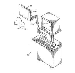
FIGURE 1 shows the camera and im~in~ system of the present invention.
FIGURE 2 shows the camera and im~E~in~ system of FIGURE 1, showing the detector,signal p,ocessol, data acquisition system, and image processing col~yu~ system of the
5 present invention.
FIGURE 3a shows an exploded ~ ec~ive view of a detection module used in the
detector shown in FIGURE 2.
FIGURE 3b shows an exploded pc.:,~e~ e view of an altemative embodiment of the
detection module shown in FIGURE 2.
10 FIGURE 4 shows a block diagram ofthe detection module board shown in FIGURE 2.
FIGURE 5a is a block ~ gr~m of the detection modules used in the detection module
board shown in FIGI)RE 4 showing the il,t~rconn~c';on of signals between analog and
digital ASICs used to implement the detection module functions.
FIGURE Sb is a simplified bloclc diagram of a fall-through circuit used to read valid
15 events recorded in the detection tolt-m~ont conditioning and p~oces~ g ch~nnçlc of the
present invention.
FIGURE 6 shows a bloclc diagram of the analog ASIC shown in FIGURE Sa.
FIGURE 7 shows a block diagram of the digital ASIC shown in FIGURE Sa
CA 02208576 1997-06-23
WO 96/20412 PCT/US95/16911
FIGURE 8 shows a fim~l n~l block ~iagr~rn of the signal ~.~,ce~so~ shown in FIGURE
2.
FIGURE 9 shows additional details of the signal ~OCeSSOI of FIGURE 8.
Like ~ef ~ nce numbers and ~esi~T ~tions in the various drawings refer to Iike e~ ont.~.
CA 02208576 1997-06-23
W O 96/20412 PCTrUS95/16911
-12-
DETAILED DESCRIPTION OF THE INVENlION
Throughout this description, the ~Lcfell~d embodiment and examples shown should be
considered as exemplars, rather t~lar as limit~tion~ on the present invention. The
following d~s~ption ~esr~ib~s ~etection of gamma rays, however, the detection of x rays
5 can be equally con~id~red. Many x-ray applications would require dirr~.e.lt ~im~n~ions
of the sub-coLuponc~L~.
The semicon~ctor-based garnrna-ray camera and m~lic~l im~ging system of the present
invention, he.e;~LI~ referred to as a "camera," is shown in FIGURE 1 and referred to by
~cf~ ce nnm~l 100. Reft ~ing simlllt~n~-ously to FIGURES I and 2, the camera 100
10 ofthe present invention compri~ps a gamrna-ray detector 200, an entrance apelLulc such
as a colIimator or pinhole 205 for directing the gamrna rays to the detector, a signal
processor 300, a data acquisition COLU~U~,r 400, an irnage proc~s~ing co~ uLel system
450, and a gantry 500 for positioning the camera adjacent to a patient7 an organ, or other
object 102. The ~letPctor 200 is used to sense r~ rion e_itted from the object 102. The
signals ge .~ rd by the detector 200 are ~ d to the signal processor 300 using any
convenient means, preferably a digital communications link 202.
As shown in FIGURE 2, the camera 100 also preferably int~ s a pluTality of
input/output devices for 1.,~ ...;LI;.~g and displaying derived images of the object 102 to
both on-site and remote users ofthe present invention. For example, the present camera
20 100 preferably includes, at a minimum, an input from a device such as an
ele~;hoca~ liograph and a display device 604 for displaying images ofthe object 102 to on-
site users (not shown). However, images can also be tr~n~m~ to off-site or remote
users via a teleco., l. "u.~ic~ions L~. .wo~h 616 using a f~c~imile m~chine 600 or a modem
602 or direct digital r.elwu~k (not shown). The camera 100 can produce "hard copies" of
25 images using a plurality of paper display de~ices. For example, the camera 100 can
include a laser printer 606, a dot-matrix printer 608, and a plotter 610 for providing paper
CA 02208576 1997-06-23
PCT~US95/16911
W 096/20412
-13-
or filrn copies of an irnage. The carnera 100 can also store ~igiti7~d irnages of the object
102 in a magnetic data storage device 614 and/or an optical data storage device 612.
Both planar and single photon ernission coLu~uLed tomographic (SPECI ) irnages of the
ernission of radiation from radioisotopes are obtainable using the present camera 100.
5 The camera 100 is ~ci~ne~l to provide images of areas that are difflcult to access and
image using COll~ ;on~l garnma cameras. The camera 100 is also r~ecign~rl to provide
images that are coLI~nLionally obtained in nuclear medicine. As shown in FIGURE 2,
the gamma-ray detector 200 preferably comrric~s an array 204 of detection modules 206
mounted upon a module board 208. The module board 208 transmits the signals
10 generated by the detection modules to the signal processor 300 for procescing. As
described in more detail below with leftl~ nce to FIGURES 3-4, each of the detection
modules 206 includes detection elem~ont array 212 which comprise semiconductor
m~t~ri~l that can detect gamma radiation with acceptable p~lrullllance at room t~LU~ld-
ture. In addition, each tletec~ion module 206 includes ulL~dted circuits (ICs) in a carrier
214, o~ Livdy coupled to the detection elements 212, that amplify, condition, and
process the electrical signals g~ ,,t~d by the detection elements for tr~ncmiccion to the
sig~al processor 300. The sig~al processor 300 ac.luu~ the signals from the gamma-ray
detector 200, makes corrections to the data, and places the data into memory for use by
the data acquisition coLul.uL~ 400 for fu- 111 ;n~ images of the object 102. The irnages are
displayed on the display 604 and stored, printed, or LI~L liLLed using the other output
devices shown in FIGURE 2. The sig~ificant coLu~olle,.L~ of the camera 100 are
described below in respective sub-sections.
G~mm~-Rav Detector
The gamma-ray detector 200 of the present invention comprises an array of closely-
packed detecion modules 206 mounted upon the module board 208. The module board
208 routes the signals generated by the detection modules 206 to the signal processor 300.
The detector 200 preferably includes an 8X8 array of detection modules 206. For
-
CA 02208576 1997-06-23
PCTrUS95/16911
W 096/20412
-1
conve~ience of ples~ AI ;on, FIGURE 2 shows a 4xj array of ~tection mod~es 206.
The ~etection modules 206 are preferably ~im~n~ion~ 1-inch by 1-inch square.
Therefore, the ~efe,L~d embodiment of the gamma-ray detector 200 has an "active"sensing area of 64 square inches.
5 Another embodiment of the present invention mounts the detection modules 206 in a
shape other than a plane to form a detectinn surface that is more a~pro~liate for imAging
some objects. Also, although the illustrated embodiments desrribe a detector 200 having
detection modules 206 arranged in an array format, the present invention con~ plates
detectors 200 including detection modules 206 a~Tanged in other configurations. For
10 example, the modules 206 can be arranged linearly, or in a circle, or in any other
convenient configuration.
The module board 208 and the ~tection modules 206 of the ~etector 200 are housedwithin a light-tight housing. Shi~l~ing mAt~ri~l preferably lead, is positioned behind and
on the sides of the module board 208 and detection modules 206 to prevent stray rArliAtion
15 fiom adversely affecting the acquired image. The shields are Al~ A~;~/ely made of
tungsten carbide or other high-density m~tPriAI and have sufficient mass to block
ullw~Llt~d stray r~iAtion from reaching the detection ~ --f .I~'i and thereby degrading the
quality of the images produced by the camera 100. The housing (not shown) also
preferably includes a thin ~ lll window which is positioned over the face of the20 detection modules 206. The window prote~ the detection modules from light andphysical damage yet allows gamma rays emitted from the object 102 under test to
penetrate the window and to be absorbed in the detection elements 212. Alternatively,
the window can be made from any low Z mAt~riAI which does not absorb an appreciable
amount of the radiation being imaged.
The housing is secured around the module board 208, detection elements 206, and
shielding mAt~ri~l using screws or other ~llArh",~ ~I means. The digital co~ ications
CA 02208576 1997-06-23
W O 96/20412 PCTrUS95/16911
-15-
link 202 enters the housing L~o~ a hole or slot (not shown) formed at one end. The
slot a~d the housing edges are preferably made light-tight. The housing is preferably
su~polled to the gantry 500 using vibration isolation techniques. In one l~cf~ dembo-limPnt the t~ e within the housing is controlled by a cooling system which
S removes heat from the housing.
The dead region around the active surface at the detector is small. It is made up of the
5hiPlrling m~te~i~l on the sides of the detector and the support housing, and it is typically
less than 0.5 inch.
Detection Modules~0 FIGURE 3a shows an exploded pe ~ .e~ e view of one detection module 206 of the
Sc~ll invention. As depicted in FIGURE 3a, the detection module 206 c~.,.l,. ;~es an
il,tc~ated circuit mounted within a l-inch square ceramic or plastic carrier. The
semiconductor ~etection m~tPri~l, sub-com~o~1c.lt 210, of the detection module 206
incln~s an array of detection çlPm~ntc 212. The detrction elements 212 are preferably
15 configured in an 8x8 array. In the prcfc.,cd embodiment of the present invention, the
detection elements 212 comrriee a plurality of c~l~iu~-zinc-telluride (CZT) garnma-ray
detection areas formed on the lower surface of sub-colllpo~ent 210. The crystals can
~ltprn~tively c~mrrieP c~millm tell-lrid~P, mercuric iodide, g~ .., silicon, or other
x-ray or gamma-ray se~lsi~vc m~teri~le As is known in the art, CZT crystals provide
20 good energy and spatial resolution, can operate at room tc~. ~al~c, and can be m~nllf~r-
tured in large volurnes in a variety of ~imeneions. The CZT crystals convert gamma rays
received from an object under test 102 (FIGURE 1) into electrical charge pulses. The
~mplit~ ç ofthe electrical pulses are indicative ofthe energy ofthe gamma rays absorbed.
The clet~ection modules 206 shown in FIGURE 3a is assembled with thin plates positioned
25 on both the top and bottom s~lrf~res of the sub-component 210. The upper plate (not
sho~,vn) provides a means for applying a bias voltage to the detection modules 206,
CA 02208576 1997-06-23
PCT/US95/1691 1
WO 96~ 12
-16-
in~ tl-s the bias voltage from the detector housing, and provides physical prol~clion for
the CZT crystals. The upper plate is d~ci~n~d to allow the gamma rays ernitted from the
object 102 to ~ ' h~t~ the plate and to be absorbed in the detection Clt .~.lt~ 212. In the
y~fi ~l~d embo-iimtont the plates are made from 0.5 rnm thick ~lumin~ ~It~m~tively, the
5 upper and/or lower plates are made from glass epoxy circuit board or other inc~ tin~
m~tPri~l A lower plate 230 provides the means for con~ g the detection çl~ 212
to the circuit carrier 214. The lower plate 230 includes a plu~ality of contact pads 232
which co.l~y.~ud in position to the positions ofthe detection elements 212. The plurality
of contact pads 232 provide electrical connection for each detection element to a
10 coll~yo~ g input contact pad on the top surface of the circuit carrier 214. The contact
pads 232 are electricalIy isolated from each other.
The circuit carrier 214 houses the ICs and passive co,~ o~ ;, and provides illL~;u~ec-
tions from the ICs to the detection elements 212 and to the module board 300. The circuit
carrier 214 preferably comrricçs ceramic or plastic. In the preferred embodiment, thick-
15 film resistors and ~ p~cil~ in the circuit carrier ~ 14 couple the signals from the detectionelements 212 to the inputs ofthe ICs and shunt detector leakage current to ground.
In the ~le~ ;d embodirnent of the present invention, the electrodes of sub-coll~onent
210 are formed by a gold layer on the CZT. ~lt~ tively, pl~tinllm, carbon, or other
conductive m~teri~lc can be used. The rl~tection ~ om~ontc 212 are formed by an array of
20 electrodes on the lower surface of the sub-component 210. The spatial resolution of the
gamma-ray detector 200 (FIGURE 1) is det~ d in large part by the size of the
detection elements 212. ~e. r~ e and long-term stability are enhanced by passivating
the areas of CZT crystal between the electrodes.
In an ~It~n~tive enviru--, ., It, the array of detection elpm~tc 212 fo~ned in the detection
25 module 206 compric.oc sep~ CZT cIystals, shown in FIGURE 3a as four CZT crystals
218, 220, 222, and 224. The cryst Is shown are preferably 12.7 mit~imeters by 12.7
CA 02208576 1997-06-23
WO 96/20412 PCItUS95tl6911
-17-
millimet~r_ by 3 millim~t.ors thick, comrncing spec~al grade CZT. Gold contact films
or layers are affixed to top and bottom ~uLf~es of each crystal 218-224. The electrodes
on the bottom surface of each crystal form a pattern of gold squares, one square for each
detection ele n~nt In the ~ d emborlimpnt~ the gold squares are approximately 3
S millimeters on a side. The lines of separation 216 h .~. n the squares are preferably
passivated, thereby, producing greater than 100 megohms isolation between detection
el.om~ntc
In the pl~f~.led embodiment, conductive epoxy is used to bond the electrodes of the
det~ c~on ~1~ ml~ntc 212 to the contact pads ofthe lower plate and the co~ of the lower
10 plate to the input contact pads of the circuit carrier 214. ~ ItPrn~tively, other conductive
bonding means may be uced such as indium-bump bonding.
Thus, the detector inputs are conn~cte~ to the ICs in the circuit carrier 214 via the upper
surface of the carrier 214. Other inputs and outputs are connected to the ICs via a
plurality of pins 240 on the bottom surface ofthe circuit carrier 214. The plurality of pins
15 240 are ~eci~n~ ~ to mate with insertion or socket CQ.~I-P~ aff~xed to the module board
208 (FTGURE 2). As described above, prior art assemblies of semiCon~ r~tQr radiation
dclcclol~ typically ;--~t;, r~re with conrli~oning electronic circuits in a manner that allows
the assemblies to be butted on, at most, three sides. The configuration of the detection
module 206 shown in FIGURE 2 advantageously allows the detection module 206 to be
20 butted on all four sides. Th~.efole, the present detection module 206 advantageously
provides a modular el~rn~nt which can be combined in a number of ways with otherdetection modules 206 to produce a nuclear medicine imager having a desired configura-
tion.
",.I;~ely, FIGURE 3b depicts the same detection module 206 but with the array of25 semiconductor de~ection elements 213 formed by orthogonal strips on the upper and
lower ~". r~ s of sub-co.llpone.lt 210. An advantage of using orthogonal strips is that the
CA 02208576 1997-06-23
WO 96/20412 PCT/US95/16911
nurnber of ~h~....~lC of signal con~itioning is less for the same spatial resolution or the
spatial resolution can be made finer with the same number of ~h~nnt~lc of signalcon~ oning In this embodiment, the signals from the upper surface are cQ....~cl~d to the
inputs of the ;.~ d circuits via a capacitor and resistor network. The ~ e
5 embodiment shown in FIGURE 3b preferably has 32 upper strips and 32 lower strips on
1 mm centers in a module that has outer ~im~ncions of a~lo~ cly 32 mrn by 34 mm.The module has a small dead space at only one edge and is constructed to ~ i7e that
dead space to allow the module to be fully buttable on 3 sides and buttable on 4 sides with
a small dead space on only one side. The semiconductor m~tt~ri~l is made up of one or
10 more elements with strips formed on the ~... ri~ es and ~t~.co...~l-cte~l as required to form
the total array.
CZT crystals have been comm~rcially available from Aurora Technologies Col~olalion
of San Diego, C~lifomi~ since the late 1980's and from eV Products of SaYonburg,Pe~sylv~ia since 1993. Cadmiurn telluride is available from vendors in the U.S.A.,
15 Asia, and Europe.
Pasaiv~tion of CZT Dclcclula
In the prcf~lcd embodiment of the present invention, the areas of passivation on the
~ r~ s ofthe CZT su~co~ on~ ~l 210 are created by for~ung an insulating film on the
CZT. In the plcf~"~d embodiment, a native oxide film is grown from a substrate of
20 cadmium zinc telluride after the metal layer has been deposited upon the substrate
~ ri1c~s Growing a native oxide film provides a means for ~oncl-ring that the resict~nce
between metal pads or lines formed in the sub-ct~t~ is increased and m~int~in~(l at a high
value.
The inclll~ting film layer 216 (FIGURE 2) is formed in a CZT surface by treating the CZT
25 surface with a hydrogen peroxide solution at low te~l.pe.~ cs. After the metal layer is
deposited, a native oxide layer is grown by subjecting the CZT substrate to an aqueous
CA 02208576 1997-06-23
PCTrUS95/16911
W 096/20412
-19-
hy~oge.l peroxide solution of aE~lu~ ely 3% to 30% conce.lL aLiorl at te~ dLu~S
of ap~l~x;. ~ ly 20 ~C to 60 ~C for a~l.lu~ rly tvvo secon~c to an hour depending upon
e. For example, the CZT ~etec~ion t?lern~nt array is preferably first m~t~lli7~dand ~ ;l before being c~ osed to the aqueous hydrogen peroxide solution.
S Typically, the CZT sub-co~ollent 210 is placed in an aqueous hydrogen peroxidesolution of a~p~u~ately ;% conc~ontr~tion for a~lu~ately 30 mim~tes at 60~C.
However, the Lr~ ~ ~p~ ~1l l l. e may vary depending upon the desired depth of the ûxide layer
and the speed at which the oxide layer is to be grown. After exposing the CZT substrate
as described, a black, highly-resistive oxide film is produced upon the surface of the CZT
10 substrate which sllbst~n~i~lly decleases surface leakage ~ le~lts between the detection
elements 212. The leakage current can be further decreased by baking the passivated
detection elements 212 in an oxygen-nitrogen en~ u~ cnt at relatively low te~ .dlul. s.
For e~mple, the passivdted detection elementc are typically baked in air for approxi-
mately 30 " li-,~ s at a t. ,llp~dlure of appro~cim~tely 60~C.
The oxide film 216 between the detection elem~ntc 212 is soluble in hydrogen chloride
solutions. The film may also be dissolved in an acidic aqueous HAuC14 electrolytic
plating solution typically used for contact metallization. It is i~luoll~t to be able to
dissolve the oxide fiIm when the CZT detectors are fabricated by pas~iva~ing the CZT
wafers before m~t~lli7~tion. In addition, dissolving the oxide fiLm is helpful when
20 selectively removing the oxide layer for metal deposition, and in a combined oxide-
etch/metal plating process.
The present method of passivating the surface of the CZT detection crystals resolves
known problems associaL~d with photûlithography for a number of reasons. Monolithic
array structures produced by phûtolithography suffer frûm low surface re~ nre between
25 metallized contacts, a~patenLly due to an alteration of the stoichiometry and other
chemical effects. Surface effects produced by photolithography are troublesome in
monolithic array devices. Also, passivation of the edges enhances the capability of a
CA 02208576 1997-06-23
PCTrUS95/16911
W O 96/20412
-20-
single c1~ detector or of an array detector to operate at high voltages, and de~ lcases
leakage .;u..~ . The problems produced by photolithography are alleviated by thechernical passivalion method dçscribe~ above. By l~hPmi~11y passivating the CZT
surface, the present invention offers signific~nt ad/~es over the prior art. For5 exarnple, a native grown in~ ting layer elimin~tl-s the problems associated with
depositing an oxide layer upon the CZT substrate. In addition, CZT crystals having a
native oxide layer can be easily and iue~e~iv~ely m~n~1f~ct lred. The oxide layers
provide high resistivity and decreased surface leakage c~rent between the detection
elements 212. In addition, the native oxide is chemically co...~ ;ble with the CZT
I 0 substrate.
Detection Module Board
FIGURE 4 shows a block ~ ~ m of the ~etPction module board 208 shown in FIGURE
2. The detection module board co~La~s an array of socket con"~clol~ into which each
detection module 206 shown in FIGURE 2 is inserted. ~1t~m~tively, the modules can be
15 soldered into the module board. FIGURE 4 shows the illh.co~uection of the detection
module input/output pins. In one embodirnent, the gamma-ray detector 200co~lises35 detection modules arranged in a 5x7 array. However, the array size used in the
ill~L aLed embodiment is exemplary only, and should not be taken as a limitation of the
present invention. The gamma-ray detector 200 of the present invention may comprise
20 X detection modules 206, arranged as an NxM array or as any shape or size. The only
dif~erence between such an NxM array camera and the ill~hdtt;d embodiment example
is the way the modules are mapped in the image and the number of address lines required.
For example, in one embodiment, six address lines specify the location of sixty-four
detection modules 206 ~ ged in a square pattem. The same sixty-four elements could
25 also be arranged in any other desired shape, such as rectangular, circular, as an angular
ring or a cross. In an embodiment having a 16X16 array of detection modules, eight
active lines are required on the module address bus 256.
CA 02208576 1997-06-23
WO 96t20412 PCTIUS95/16911
Each ~etec~ion moduIe 206 shown in FIGURE 4 is mated to a co~ ,o~ding socket
co~e~ilor (not shown) soldered or otherwise affixed and electrically coupled to the
moduIe board 208. The sockets are closely packed together on the moduIe board 208
with the detection modules 206 butted against each other on all four sides when the
5 modules are fulIy engaged and mated with the 5O~ PtC The module board preferably
includes "push holes" (not shown) at each module location which allow a technician to
instalI or remove the modules 206 from the sockets without damage during testing and
servicing.
Both digit 1 and analog signals are routed in a known fashion to each socket via traces in
10 the module board 208 as s~h~o~n~tically shown in FIGURE 4. The digital signals and
supply lines are provided to the module board 208 via input and output ports that are
co.-nP~-~e~l to the digital cou~u~cations link 202 (FIGURE 2). As shown in FIGURE
2 and described below in more detail with refe ~ --ce to FIGURE 8, the digital commllniç~-
tions link 202 is connected to the signal processor 300. The analog sign~lc, output by
each detection module 206, are bussed together on the module board 208 and routed via
linear buffers 250, 252 to the signal processor 300 (FIGURE 2) via an analog link 203,
preferably a twin-axial cable. The cross-talk between the analog and digital signals is
thereby greatly reduced by conditioning and chiekling the analog output signals and by
L~ g the analog and digital signals over s~&dte cornrnunication Links 202, 203.
20 In the embodiment shown in FIGURE 4, the detection modules have a plurality of
input/output pins 240 (FIGURE 3a) which mate with corresponding insertion connectors
in the module sockets affixed to the module board 208. The pin-fimction list for each
module socket of the illustrated embodiment is given below in Table 1. Pins and
functions listed below have co~le~olldi.lg integrated circuit inputloutput fimctionality as
- 25 is described below with .~r. ~ nce to FIGURE 4.
CA 02208576 1997-06-23
PCTrUS95/16911
W 096/20412
-22-
Ground co... ~l ;onc~ bias signals, and supply voltages are routed to the detection m~ s
206 via internal layers of the ~letection module board 208. Power pins are col---e~-led to
bypass capacitors (not shown) which bypass the power supplies to les~c.,Li~e ground
planes. Digital and linear signals are l,u~ d on both the module board 208 and on the
5 signal processor 300 (FIGURE 2). Table 2 shows the pin function list for the digital
cc~ tionc ~nk202 which couples the module board 208 with the si~ processor
300.
CA 02208576 1997-06-23
W O 96/20412 PCTAUS95/16911
-23-
P~ NCTION
¦ INPUT/OUTPUT ¦
1-6 Element Address Output
7 FallIn Input
8 FalI Out Output
9 Valid Output
Address Enable Output
I l Advarlce Input
12 Linear Reference Output
13 Linear Ou~:put Output
14 Threshold Input
Threshold Re~.e.lce Input
16 Analog Power #1 n/a
17 Analog Ground #l n/a
18 AnalogPower#2 n/a
19 Analog Ground #2 n/a
Digital Power #2 nla
21 Digital Ground #2 n/a
22 Test Signal (Linear) Input
23 Test Shift Register CLK Input
24 Test Shift Register Data In Input
Test Shift Register Data Out Output
TABLE 1 - Detection Module Pinout Function List
CA 02208576 1997-06-23
PCTrUS95/16911
W 096/20412
-24-
F~CTION INPUT/OUTP-
1-6F.lemen~ Address Output
7-14Module Address Output
Valid Output
16 Advance Input
17 Threshold I~put
18Bias Voltage n/a
19Analog Power n/a
20Analog Ground n/a
21Digital Power n/a
22Digital Ground n/a
23Buffer Power n/a
24Buffer Power n/a
25Buffer Ground n/a
26Chassis Ground n/a
27Test Signal input
28 Test Data input
29Shift Register ~1 input
30Shift Register t~2 input
TABLE 2 - Wire List for Link 202
CA 02208576 1997-06-23
WO 96J20412 PCT/US95/16911
In the plef;,l~1 embodiment, tne signals provided from the signal ~lucesso~ 300 to the
detection module board 208 include voltage and ground refere~ces and the "advance"
signal. As desrnbe~ below in more detail, the address and "valid" signals and the analog
outputs are provided from the detecion module board 208 to the signal processor 300
S when a fall-through addressing id~nhfi~s a valid event in a detection el~mPnt 212. These
signals are bussed to every detection module 206 on the module board 208. For eY~mrle
all of the valid lines of the detection modules 206 are bussed together on line 260. The
bias voltage (preferably 200-500 volts) is connPcted to the top surface of each detection
module and excites the detection elements 212 during camera operation.
10 Both module and element addresses are supplied to the signal processor 300 via comrnon
address lines 256, 262 co~ ected from each detection module location on the module
board 208. The module address bus 256 and the elem~nt address bus 262 are logically
combined to create an n-bit wide address bus. In the p.c;f:_,.ed embodiment, the address
bus I ~ to the signal processor 300 is l~bits wide. In the ~refe~.~d embo~lim~?nt,
the module address lines 256 are treated by the signal processor 300 as the most-signifi-
cant-address bits, and the element address lines 262 are treated as the least-significant-
address bits. The address busses 256, 262 are driven by tri-state buffers at each detection
module loc~non Only one detection module 206 asserts an address on the address busses
256, 262 at a given time.
20 In the ~lcfe,l~d embodiment, the module address of each detection module 206 is "hard-
wired" into a tri-state ~scei~er located at each module on the module board 208. That
is, the binary address for each module socket is pre-wired by connecting the apyl~pliate
bits to digital ground and power. As described below in more detail with reference to
FIGURES 5-7, when the fall-through addressing arrives at a detection module with valid
25 data, that module outputs an analog signal (via a linear signal out line 270), a "valid"
signal, an "address enable" signal, and the address which uniquely id~nt-ifi~s the detection
~l~m~nt 212. The digital IC in the detection module 206 asserts the detection element
CA 02208576 1997-06-23
WO 96/20412 PCI~/US95/16911
address on the address bus 256, and a tri-state address buffer at that module location
asserts the detection module address on the bus 262 when an "address enable" signal is
asserted true. The detection modules 206 are the.efo,e ~esign~ to be completely
interchangeable. The detection modules 206 the.~fc"~c are not "addressed" by the data
S acquisition co~uull-~ 400 in a conventional sense. Rather, as described below in more
detail with lcf~ ce to FIGIJRES 5-~, the modules 206 initiate the address when an event
occurs. As shown in FIGURE 4, the detection modules 206 are linked together in a"daisy-chain" configuration by couplLng the "fall-out" output signal from one module
(e.g., fall-out signal 280) to the "fall-in" input signal of a successive module (e.g., fall-in
10 signal 282). As described below, the "fall-in" and "fall-out" signals are used to implement
the "fall-throu~h" data scheme of the present Lnvention.
As ~esrribed below in more detail, when a detection module 206 asserts a valid signal on
line 260, the signal processor 300 reads and plocesses that detection element's address on
the "address" lines and analog signal on the "linear output" line. The signal p~cessor 300
15 then re-init.~tt s the fall-through adL~s~g and data acquisition process by generating and
s~n~linP an "advance" signal overthe digital c~.. ,.. "ications link202.
~etection Modules ~ o~ ection of the An~log ~nd Di~ital Tnt~rated Circuits
The circuit carrier 214 preferably co~ c three ;..t~.,.t~ ci~ two identical analog
application specific integrated circuits (ASICs) and one digital ASIC. The two analog
20 ASICs arnplify and shape the analog signals for processing by the digital ASIC. The
digital ASIC co~, es the analog signals ge .~ ~r~ by the analog ASICs with a reference
or threshold voltage. If the signal is greater than the threshold (a "valid hit"), a latch is
set which causes the analog value to be stored in a peak detection circuit. When enabled
by a fall-through signal, the digital ASIC generates a "valid" signal and an "address
25 enable" signal. L~ ,conl~;~ions within the detection module 206 between the two analog
ASICs 700 and a digital ASIC 800 are shown in the block tli~ m of FIGURE ja. The64 signals from the detection elements 212 are connPctPd to the inputs of the analog
CA 02208576 1997-06-23
W O 96/20412 PCTrUS95/16911
ASICs via thick-film r~ JIS in camer 214. The leakage current from each ~letection
ele~c.lL 212 is routed to ground via thick-film resistors so litho~Qph~d on the carrier
214.
Although the present invention is shown having t~vo analog ASICs 700 in each detection
module 206, one skilled in the art will ay~fe-e;ate that the signal conditioning functions
p~,lru~ ed by the analog ASICs 700 can be irnplemented in an QltemQtive embodiment
within one ASIC 700 and that the number of analog chan-lels in one ASIC 700 couId be
either greater or less than 32. Further, the present invention co~Lc;.,lplates combining the
analog and digital processing fiml~hon~ on a single ~te~ated circuit.
Because the detection elem~ntc 212 produce low Qmplit~ e electrical pulses when
irr~-liQtç~ any noise created during the proc~csing of these signals can adversely affect
the resultant image. The present invention ~ignifiçQntly reduces crosstaLk and noise by
se~Lil~g the analog and digital ciLc~iL~ y into sep~ nte ASICs.
Some prior art imQging devices use ASICs that re~uire that the preQmplifier associated
with each detechon element 212 be reset periodically to coLu~e~sale for detector and
~mrlifiPr input ~ . This resetting is typically acco. . ,pli~h~d with an analog switch
co~lne~;t~d across the preQmplifier fee~bQ~k path. The operation of the switch causes
large, spurious signals and mo."P .I~. ;ly in~QpacitQtes the amplifier. Passive fee~lbQck
n~ olks are difficult to implement bec~.~se high re~i~tQnce values must be used to
effectively reduce the noise levels. The pro~llction of such high-value resistors is not
c~ ly possible. As shown in FIGURE 5a, the present invention el;lll;l~tes the detector
current portion of this problem by placing a resistor/capacitor network 702 be~veen an
input port 704 and its associated input pad 706 on each input of the an~og ASIC 700.
The resistorlcQrQcitor ne~wulh702 shunts leakage current from the ~etec~ion element 212
to ~ anlog ground 712 on the module board 208 before the leakage current enters the
analog ASIC 700. Typical values for the resistor 708 and the capacitor 710 of the
CA 02208F776 1997-06-23
WO 96/20412 PCTrUS95/16911
-28-
~eji~Lol/c~p~--iLo. n~.w~lL 702 are 200MQ and 100 pF, re~,uc~;Li~ely. The amplifier input
current is co~ ed by using a high output iu~pcdallce arnplifier as the feedb~rk
element around the preamplifier. Each detection el~mtont 212 of the 8x8 array of each
detection module 206 iS electrically coupled to an input port 704 on the circuit carrier
214. The signals g~ ~d by the ~1P ~ch~n elf~fn~8ntc 2l2 and t~ .c.~.iLll~d to the 64 input
ports 704 are relatively low-level signals ranging in values from 6000 to 60,000 electrorls.
Assertion of the valid line 260 by one of the detection modules 206 indicates that at least
one of its detection elements 212 has received a hit that ~ uucs processing and that it
was selected by the fall-through addressing. Following a valid hit and after waiting a
short time period which is sufficient to allow the linear signal to stabilize within the peak
detector, the digital ASIC 800 enables an intf m~l gate and waits to be enabled by a fall-
through signal which is described below in more detail. Valid hits can be con.;ul~ y
stored for all detection elements 212 in the ~f~tecrion module 206 by the digital ASIC.
After a detection element 212 receives a valid hit, it waits to be enabled by a fall-through
signal. The ASIC 800 then asserts a "valid" signal on output line 260 and an address
enable signal on output pad 831. As described above and shown in FIGURE 4, the valid
lines 260 of all of the detection modules 206 are electrically coupled together and the
valid signal is ~ ed to the signal processor 300 over the digital coll~ullica~ons
link 202.
Thus, if any of the ~etech~n ek ~ ; in the gamma-ray detector 200 produce a valid hit,
the valid and address enable signals are asserted for that detection element when it is
enabled by the fall-through signal. A peak detector in each ch~nnf l of the digital ASIC
800 stores the amplitude ofthe charge pulse received from the detection çl~m~nt 212 until
it is read by the signal ~lucessor 300. As shown in FIGURE ~a, the stored analog signal
is provided to the signal ulucesso~ 300 through an analog pad 817 which is coupled with
the linear bus 270. The hit is held within the digital ASIC 800 untiI it is read, processed,
and cleared by an advance signal 258 produced by the signal processor 300. Each peak
CA 02208576 1997-06-23
W O96/20412 PCTrUS9~/16911
-29-
detector within the digital ASIC 800 stores the ~mplit~lde of the highest amplitude of
sl~ccessive hits generated by a detection el~m~nt 212 until it is reset by the signal
processor 300. The "hold droop" of the peak detector is preferably apl,lo~ately no
greater than 0.0001 % per microsecond.
5 When the signal processor 300 completes processing the event, it asserts an "advance"
signal on advance signal line 258. As shown in FIGURE 4, the advance signal line 258
of each module 206 is electrically coupled together. When the advance line 258 is
asserted true, the active detection module 206 (i.e., the detection module which ~lesellLly
has control of the address busses 256, 262 and the linear bus 270) clears the active output
10 lines (valid line, address lines, and linear signals) and allows the fall-through signal to
advance to the next latched detection elt?mPnS
Fall-shrollph Circuit
A fall-throug_ circuit is included in ASIC 800 for each detection element. A simplified
block diagram of the fall-through circuit is shown in FIGURE 5b as a series of logical
15 "AND" and "OR" gates coupled together. This depiction of the fall-through circuit is
given simply to describe its function. Each detection elt m~ns 212 has a colL~onding
latch within the ASIC 800 for storing valid hits received by the detection element 212.
For example, as shown in FIGURE 5b, latch 808 stores a hit received by the firstdetection çll nl ,l (DE 0), latch 810 stores a hit received by the second detection ele~nPnt
20 in the 8x8 ~Tay (DE 1), and so on. The latch outputs are coupled to co~ onding fall-
through blocks 812, 814. Block 812 has a first input of its OR gate 816 coupled to the
fall-in signal line 282. The fall-in and fall-out signal lines of the detec~ion modules 266
on the board 208 are "daisy-chained" together (FIGURE 4). For example, the fall-out
signal line 280 of detection module 266 is coupled to the fall-in input 282 of the next
detection module 268. The last detection module 284 of the a~ray of detection modules
206 has its fall-out line 280 coupled to a NOR gate 286. The output of the NOR gate 286
is coupled to the fall-in input 282 of the first detection module 266.
CA 02208576 1997-06-23
WO 96/20412 PCT/US95/16911
-30-
Therefore, the fall-through circuits within each detection module 206 of the garnma-ray
detector 200 are a~l tied together, forrnin~ one circular fall-through loop. The NOR gate
286 allows the fall-through system to be initi~li7~1 during a power-up sequence. For
example, at power up, a PWR UP signal 288 is asserted high which causes a one-shot
multivibrator 290 to de-assert a logical 0 pulse on the fall-in signal line 282 of the first
detection module 266. Refi ~ring again to FIGURE 5b, if the first detection element latch
808 of the first detection module 266 is not set (i.e., the first detection element 212
associated with the latch 808 has not received a valid hit), the OR gate 816 will output a
logical low value. The logical low is input into an OR gate 818 of the next fall-through
block 814 which is associated with the next detection element 212 of the 8x8 array of
detection elements 212 (e.g., "DE 1 "). If the next detection element latch 810 is not set
(i.e., the second detection element 212 associated with the latch 810 has not received a
valid hit), the OR gate 818 will also output a logical low value. The subsequent fall-
through blocks will similarly continue to produce a logical low value which progresses
through the chain of fall-through blocks until a detection element is found which has
received a hit and has thereby set its colfe~onding latch. If no detection element 212
within a ~etection module 266 received a valid hit, that is, if the digital ASIC 800 of
detection module 266 does not have a latch set, the detection module outputs a logical low
from its fall-out signal line 280. The low value is input to the fall-in input line 282 of the
next module 268. Thus, the logical low progresses through the OR gates of each
sl.fcee~;..g module until an el~-m.ont that has an event ready for procPs~ing is encou~ ~d
or the signal passes out of the last module and back into the first.
A logical high input to any OR gate (i.e., OR gates 816, 818, and so on) stops the fall-
through process. When an event is found, the digital ASIC 800 activates tri-state buffers
25 (not shown) which allows the ASIC to take control of both the digital address busses 256,
262 and the linear signal line 270 (FIGURE 4). The address of the detection element 212
which received the hit and which subsequently caused the fall-through circuit to halt is
output onto the element address bus lines 262 by the ASIC 800. The address of the
CA 02208576 1997-06-23
WO 96/20412 PCT/US9S/16911
ASIC's detection module 206 is also ass~ d from the ~ ccciver onto the module
- address lines 256 by the address enable line 832. As described above, the module address
is hard-wired on the module board 208 into an 8-bit ha~sceiver that is enabled by the
address enable signal. The analog signal ofthe detection Pl.oment 212 which caused the
5 fall-~.,~ process to halt is sPlected using the ~etPction element address output 262 of
the digital ASIC 800.
The valid signal resulting from a hit causes the signal processor 300 to read and process
the address and the analog signal. No other detection module can access the bus lines
because the fall-through configuration ensures that only one detection module 206 is
10 enabled at a time. The fall-through process remains halted until the signal processor 300
completes proce~sing the event and asserts an "advance" signal over the advance signal
line 258 which is shared by every detPction module. When the active ~letection module
receives the advance signal, it ~l r~.".,~ the following functions in se~lu~lce: resets the
peak detector which is ~;u~ Lly addressed; it de-asserts the valid signal causing the valid
15 signal line 260 to assume a logical low value; it de-asserts the address enable signal; it
disables its tri-state buffers, thereby, relP~ing the address and signal busses; and it asserts
a logical low pulse over its fall-out line. The fall-through process resumes with the next
fall-through bloclc in the digital ASIC 800.
Because the fall-through scheme scans detection element~ in a sequential manner, one
20 Ple ~ at a time, ~etection r.l~ . "~. ,t i 212 that receive a valid hit cannot affect or illh.~ ulJt
the sc~nning of other detec~ion elPmPnt~ All elements are "1atched-out" or inhibited until
they are read during a subsequent fall-through scan. Thus, each detection element 212
of each module 206 is given an e~ual oppo~ ~u.~y to be serviced by the signal processor
300.
CA 02208576 1997-06-23
W O 96/20412 PCTnUS95/16911
-32-
Tn~ d~c:d cirr~litc acs)
FIGURE 6 shows a block diagram of t_e analog ASIC 700 of FIGURE Sa. Preferably,
each analog ASIC 700 in~ os thirty-two ch~nnelc Each ~h~nnçl preferably has an input
pad 706 for rece;v~g and con~litioning the analog signal produced by its associated
5 detection elernent 212 when a garnrna-ray is absorbed. Each ~h~nnel includes a charge
amplifier 718 and a ch~ping arnplifier 720. The prearnplifier inco~ dLes a current-
sourcing ~mp1ifier (inrli~tl d by resistor 738 in FIGURE 6) to m~int~in the DC stability
of the circuit. The rise and fall times of the shaping amplifier are set via resistors external
to the ASIC 700.
10 The ~lef~ d value of the c~p~citor 740 is selecte~l to provide a desired delay time. The
amplifiers 718 are ~ecign~l to amplify the pulses g~ 1led by the detection ~ e..~ 212
to levels which can trigger CO-~p~o~la within the digital ASIC 800. Preferably, the
~mplifierc 718 amplif,v the ~nalog signals to levels ~p~o~ately equal to one volt.
The peaking and fall times of the ch~ring ~mplifier 720 is chosen to . .~ white and
15 1/F noise contributions and to obtain good b~celinP recovery. Preferably the peaking time
is 0.1 to 1.0 microsecond with fall times of 1 to 10 microseco~1c~ The outputs of the
shaping amplifiers 720 are coupled to the inputs of col~,J~onding peak deteclola in the
digital ASIC 800.
As shown in FIGURE 7, the digital ASIC 800 preferably includes sixty-four parallel
20 çh~nnelc coll~Jl,onding to the sixty-four detection elPmentc 212 asso~ d with each
detec~ion module 206. Each channel includes a peak detector 820, a colllpdldlor 822, an
event latch 824, AND gates 826, 828, a fall-through block 830, and an address encoder
832.
As described above with reference to FIGURE 5a, the peak detectors 820 p.,lrO~ an
25 analog peak detection function by storing the highest of successive pulses gen~.dted by
CA 02208576 1997-06-23
WO 96/20412 PCT/US9S/16911
the detection elements 212 until a valid signal "locks out" any subsequently generated
pulses. The ~ubse~ Lly g~ tr~l pulses are "locked out" untiI the peak value is read.
The switch 814 allows the analog signal from the selected peak ~et~ctor to be t~ d
to the signal processor 300 via the linear out sig line 817 when that detection element
5 address is valid.
As shown in FIGURE 7, the peak detectors 820 include control lines 833 coupled from
the fall-through blocks (830,836, 838) to the ~wit~,hcs 814. The switches 814 couple the
OUtpUt of a s~lected peak detector 820 to the signal buffer 812 when act~l~ted by a control
line 833. The an~log voltage stored by any one peak detector 820 is reset by the advance
10 signal 842 if and only if the address of that element is enabled. That is, when a switch
814 is activated by a fall-through block (e.g., 830), the peak detector connected to the
activated switch 814 is reset when the advance signal 842 is asserted. Thus, after the
signal processor 300 processes an event stored by a peak detector, it clears the selected
peak detector 820 to allow it to begin ~c~ ting subsequent hits.
The buffer/driver 812 is coupled to switch 810. The switch 810 is controlled by an
address valid signal line 848. The address valid signal line 848 is described below in
more detail with ~efe~nce to the fall-through blocks enable signals. The output of the
buffer/driver 812 is coupled to the out sig output pad 817 which is connected to the
signal processor 300 via the Linear out signal Line 270 (FIGURES 4 and 5).
20 As shown in FIGURE 7, a first input to the co~pdldtor 822 is provided via the input pad
802. A second input to the co~ d~atur 822 is provided via a threshold voltage (V~ input
line 804 which is cornmon to all modules in the system. If the detection element signal
arnplitude has a voltage that is lower than the threshold voltage, the event is not recorded.
However, if the detection-element-signal amplitude is greater than the threshold (V~,
2~ the co~paLator 822 asserts its output (preferably by asserting a logical high value at its
output) to set the co~ ,onding latch 824. The signal remains recorded in the event latch
CA 02208576 l997-06-23
W O96/20412 PCTrUS95/16911
-34-
824 until it is processed and reset by t_e signal processor 300 as ~esrnbed below in more
detail.
The AND gates 826,828 serve two di~ t timing functions. The AND gate 826iS usedto ensure t_at the pulse g. ..~ .aLed by a detection elemçnt 212is allowed to stabilize within
S t_e peak detector 820 (FIGURE 7)~ccori~t~1 with that detection element 212 before t_e
valid signal is gene~aLed. The logical one is inverted before it is input to the AND gate
826, which causes the output of the AND gate to transition to a logical low value. The
AND gate 826 output will co.,~ .o to be m~ .;n~d at a logical low value until the pulse
received by the input 802 transitions below the threshold voltage. The AND gate 826
the,c:folc pl~ the output of the event latch 824 from passing though it to the AND
gate 828 input until the pulse returns to a level below the threshold voltage. This delay
ensures that the peak detector 820iS allowed to stabilize before a hit is passed on to the
fall-through block 830. This ensures that the analog signal ~ e~l by the peak dotector
820 via out_sig pad 817 co~ o~lds to the peak arnplitude of the pulse.
The AND gate 828iS used in conjunction with the fall-through block 830 to facilitate the
fall-through scheme described above. As described below in more detail, the AND gate
828 prevents a detection element 212 which .eceives a hit from i~L~-u~L~g the fall-
through process until the detection el~m~ont is sc~nnçd by the fall-through circuit. The
AND gate 828, together with the fall-through blocks, ensures that every event latch 824
issc~nnP(l in se~ù~Lial order and that every detection element has an equal op~olluui
to be serv-iced by the signal processor 300.
As described above with reference to FIGURE Sa when the "advance" signal 258 iS
asserted on advance input pad 842, the sc~nn~od event latch 824iS reset via reset line 844.
As shown in FIGURE 7, the reset line 844 of the enabled latch 824iS coupled to the
priorit,v-select/fall-through block 830. When a selected block 830 receives an advance
sigIlal 842, the block 830 resets the latch 824 via the reset line 844.
CA 02208576 1997-06-23
W O96/20412 PCTrUS9S/16911
-35-
The fall-through blocks include "enable" outputs which are coupled to a plurality of
address en- odPrs (i.e., 832, $70, 890, etc.). AI1 enable output of a selected fall-through
block is asserted ~l~e.~ . the event latch 824 which is coupled to the sPlectPcl priority
select block co~ an event and the selected priority select block is ~ Lly being
5 sc~ (i.e., the fall-through process has reached the s~le~Lecl priority select block). The
enable outputs thereby cause one of the address encoders (e.g., 832) to present an address
on an internal address bus 846 which is indicative of the selected detecion elPment 212
co."i.,.,;.,g a valid hit. A valid address signal 848 is then as~c.lc~d which causes an analog
switch 850 to close. The detection elemPnt address is then asserted on the detection
element address bus 262 and LL~ I;LIe~-1 to the signal processor 300.
As described above with reference to FIGURES 5-7, each ~etechon module 206 has an
analog ASIC 700 which ~mplifies the analog sign~s produced by the detection ele.~eu
212 and which CO111~LC3 the analog signals with an event threshold voltage which is
commc)~ to all of the detection modules 206. The event threshold voltage is preferably
15 established above noise level. When the analog signal produced by a detection element
212 PYI~ee~1s the event threshold voltage and that detection element is "addressed" via the
fall-through scheme as described above, the digital ASIC 800 g~,dtes a valid signal 260
which infnrmc the cOlll~u~, signal plocess()r 300 that at least one detection ele,lle.lt 212
has lcceivcd a hit ~. 4u~ g p~cej~;r-g The digital ASIC 800 takes control of the linear
20 and address busses and outputs both the address of the detection elPmPn~ 212 and the
m~gnit~ e of the amplified signal. The ASICs 700, 800 clear the flag and the linear
signal produced by the addressed detection ele..lc.lt 212 once the signal processor reads
and processes the event. As described below in more detail, the signal processor 300
inflic~teS when it has ~,cessed an event by assc. Ling the "advance" signal via the advance
25 signal line 258.
Ihus, the gamrna-ray detector 200 and, more specific~lly, the module board 208 appears
to the signal processor 300 as a very simple analog/digital input device compn~ing an
CA 02208576 1997-06-23
WO 96/20412 PCT/US95/16911
-36-
array of det~tJ., which produce pulse-height and address ;.lru....AI;on and which store
this ;- fU- . I-A~ ;on until a read completion acknowledgement (via the adv~ce sig~al 258)
is provided by the signal pluccssor 300. When the signal processûr 300 has comple~cl
plOC~;"g a ~etec~ on çl~mPnt's address and reading the elc.llc.lL's linear signal, the
5 system g. ..l ,.t. ', an advance signal 258, thus allowing the next pending ~letPct on cl( mYnt
to be addressed. The next ell~mPnt in the ~etection module array which has a hit pending
will g. ~ e its address, its analog signal, and a valid flag. The signal processor 300 is
thereby freed ofthe tirne-intensive task of polling each detection element 212, including
detPCt;OnCIL~ which do not have pending hits. In fact, using the fall-through scheme
10 described above with reference to FIGURES 5-î, the addressing of detection el~m~n
occurs indepen~Pntly ofthe proc~ing p~ rO. ",rtl by the signal processor 300. The signal
processor 300 simply pulses its advance signal line 258 when it has read the detection
element event data. As shown in FIGURE 2, the signal plocessor 300 is housed on a
circuit board that ;llt~ . r;~L~S with the data acquisition co~ ,uL., 400. All co~ llullication
b~,lwcc~ the signal processor 300 and the detector 200 occurs through the
co.. ~-.. ;c~tion~ links 202 and 203.
Sun~l Processor 300
The signal pl~ce~or 300 ac.luilcs data from the gamma-ray detector 200, norrn~li7Ps and
fo----AI~ the data, and stores it in IllLJ~llol~ blocks for access by the data acquisition
CO~ uk,, 400. In additio~, the signal p~cei~ol 300 provides the bias voltage for the
~letector 200 and provides the event threshold voltage that is used by the ~e~ction module
206 for fli~ ;..g valid gamma-ray pulses.
FIGURE 8 is a func~onal block diagrarn of the signal processor 300. The sigrlal
~lucessor 300 preferably compri~Ps a field pro?~,A",-"~ble gate aIray (FPGA) 302; a flash
analog-to-digital cûn~ (ADC) 304; a fast digital-to-analog converter (DAC) 306 used
for ga~n n~rm~li7~tion; a threshold DAC 316 for setting the event threshold voltage; an
input/output port 318 for cu~ with the data ~~luisilion col~ul~ l 400; a gated
CA 02208576 1997-06-23
Wo s6/20412 PCT~US95/16911
-37-
cc~ er 314; a digital window block 322, having a low port 324 and a high port 326;
a latch 328; a test signal ge~.f ~tol 370; a one-milli~econd clock 372; and a bias voltage
supply 254. As described below in more detail, the signal processor 300 also includes
random access memory (RAM) which is allocated into several blocks: a gain memoryS block 308, a h~lù~a~ Lu~,LIuly block 310, and a pulse-height distribution memorv block
312 which are named for the type of illfo~Lu~Lion stored therein. As described below in
more detail with reference to FIGURE 9, the signal processor 300 also includes two
"ping-pong" buffers 346,348, which store addresses used in the "~ d~g mode" of data
storage.
10 All commnnir~tion signals and power b~ n the signal processor 300 and the module
board are via c~...,...~...;cations links 202 and 203. For exarnple, as shown in FIGURE 8,
the linear input line 270 is connecte~l to the linear outputs of all detection modules 206
via analog co.. ".. ;~ ;on~ link 203. The address inputs to the FPGA 302 are provided
via address lines 256 and 262; the valid line is coupled to the valid signal line 260; the
15 advance signal is provided over the advance signal line 258; the threshold voltage is
l"..l~lll;urA over the threshold signal line 272; the test signals are provided on test signal
lines 274; and the bias voltage is provided over the bias signal line 254, all via the analog
~nk 203.
The FPGA 302 allows the fimrhom of the si~al processor 300 to be controllable via
20 sGn~e. Upon initi~l;7~hon~ the data ac~uisiLion co~,~ulcl 400 Ll~ iL~ configuIation
inforrnation to the signal processor 300 via the parallel input/output port 318. This
configuration information design~tes the mode of data acquisition. For example, the
signal processor 300 can configure the FPGA 302 to store event data which exceeds a
software controlled threshold voltage in the histogram memory block 310. ~lt.orn~tively,
2S several pulse-height windows can be specified and a St~dtt: histogram can be
t~ in the histogram memûry blûck 310 for each window. Additionally, a pulse-
height distribution or s~,e~ rece;~red from each detection element 212 can be stored
CA 02208F776 1997-06-23
WO 96t20412 PCr/US95/16911
-38-
in the pulse-height memory block 312. Each of these modes can be sepA._lely specified
upon initiAIi7A~ion of the FPGA 302.
When the valid signal line 260 bf comt~s true, the detection elem~nt address is read from
the address lines 256, 262. This address is used to address a ~e~uo. y location COII~A;I~ g
5 the gain n~trrnAli7Ation factor for the cle .\f ~-t This ir.fo. ,--AI;on is l-A--~ir . .~1 to the DAC
306 that outputs a voltage ~lO~OlL onal to the element gain. The voltage output by the
DAC 306 is used by the ADC 304 in nt7rTnAIi7in~ and conver~ing the analog signalproduced by the selected proc~ccing chAnn~l and provided on line 270.
The element address is also used to map the pulse-height Amplitlldç into the histogram
memory block 310 or, Alt~rnAtely, into the pulse-height distribution memory block 312.
During an initial measul.~ent, the gain nonnAli7Ation factors are set to unity and an
isotopic source is used to measure the respollse-s of the individual elementc. These
responces are then analyzed by the host col~ er to obtain the gain factors that will be
used during imA~ing In this way vAriAnses in elem~nt ~es~ollses are eli~inA~ thus
greatly improving image quality. When the event has been acquired, normAIi7~l and
stored, an advance signal is gene,aLed on line 258 which Allows the garnma-ray detector
200 to advance to the next detection element that has a valid hit.
As described above, one important function ~ . rv.,.,to~l by the signal processor 300 is
~etection-element-gain nt rTnAIi7,ltion The sig~al processor uses the gain memory block
308 to p~.rO.~. this gain nonnAIi7Ation function. The gain memory block 308 cont~inc
a gain normAli7Ation factor for each of the detection elements in the gamma-ray detector
200. In the ~ef. ,l~d embodiment, there are as many as 256 detection modules 206 and
sixty-four detection elements 212 per module. Each pulse-height distribution comprises
128 chAnnels with a depth of two bytes. Therefore, in that example, the gain memory
block 308 has 2S6x64 x 128 x 2, or 4,194,304 memory byte locations. When an event
occurs, the gain memory 308 is addressed and the data is LLa~r~ d to the gain
CA 02208576 1997-06-23
W O96/20412 PCTrUS9S/16911
-39-
norm~li7~tiQn DAC 306. This in turn controls the; ~ f~Ous full-scale range of the
ADC 304. The output of the ADC 304 is thus "gain nl~lm~li7e~ The ADC "done"
signal 344 causes the data storage operation to proceed.
The gain nonn~li7~tion factors are initialIy obtained by first setting the factors to unity.
5 The signal ~ucessol 300 then accnm~ tes a pulse-height distribution of each ~çtection
el~Tnf nt in the pulse-height ~elllol.~ block 312. The pulse-height distnbution is analyzed
by the data acquisition co~ ul~i. 400 to obtain the relative gain for each element, a
number l,iopollional to this value is stored as a gain no~li7~tion factor for each
detection f~lP.,.~ ,I in the gain memory block 308. The gain norrn~li7~hon factors thereby
10 obtained are used to nt~ li7lo the analog signals subsequently received from each
detection ~If m~nt 212 during data acqllicition
In pulse-height mode, the element addresses and the ADC output are used to address the
pulse-height memory block 312 via address lines 340 and output lines 338 in building a
pulse-height ~ecchulll of each detection element 212. Thus, each el~m~nt address is
15 ~co~ with a 128-location histogram. The upper seven bits of the ADC specify the
"adcllcs~e~" of these 128 loc~tionc Each location in the histog~arn is incrf mentf~d by one
when its address appears on the ADC. More than one byte of memory at each location
can be spe-ifi~l for improving st~ti~tiç~l accuracy. Thus, the pulse-height memory 312
~ccl~m~ tes a pulse-height ~c~ llu~ for each of the detection elements 212 in the
20 gamma-ray ~-tecto- 200. This spe ~ Lu can be analyzed by the data ac.luisilion c~ u
400 by ~cf~ g the pulse-height memory 312.
In the image-collection modes, each detection f lf ment address is four bytes of memory
deep and is incl~ "f .~tf ~1 by one each time that address is ~l~sP"ted on the address lines
and the ADC output is of the proper amplitude. Thus, histograms of the incoming data
25 can be created accoldil~ to gamma-ray energy detecte~1 As shown in FIGURE 8, the
addresses and the event ~mplihl~s are ~ d via the address signal lines 340 and 338
CA 02208576 1997-06-23
WO 96120412 PCT/US95116911
40-
to the digital window block 322. The digital window block has a high port 326 and a low
port 324. The data ac~lui~ilion col.~ 400 establishes the va~ues provided to these
ports by wnting via the colll~ , bus 320 a low and high amplitude value into the low
and high ports 324, 326. The output of the ADC 304 is cvm~ed with the value stored
in the low and high ports 324, 326. If tbe value on the ~mpli~ldf~ lines 338 falls b~ L~
the low and bigh values stored in the digital window's low and high ports 324, 326, the
~ok~mf~nt address provided on address lines 340 is used to address the histogram memory
310. The value in the histogram memory 310 at the element address is incremente~ by
one and ~ at that address.
In "list" mode, each event is "time-tagged." Address inforrnation is combined with the
eight bits from the ADC and three bits from a clock and placed in one of a ping-pong
memory buffer pair. These buffers are sized to allow eacy data L d.,sr~r at high rates of
data acq~lici*on When a buffer fills, data transfer is switched to the other buffer and an
i~ttlLU~l is generated which sets up a DMA ~re- of the full buffer to a hard disk
optionally coupled to either the data acquisition colllpul~r 400 or the image proc~ossin~
com~ul~ system 450. An output from a port will force flushing of the buffers at the
tf "~ ;on of data acql-icition
For 256 mo~ s addressable via eight address lines in the gamma-ray detector 200, each
image histograrn requires a block of 65,536 bytes of memory (256x64x4). The signal
~locessor employs dual-ported memo~y so that both the FPGA 302 and the data
acquisition co.ll~utc~ 400 CPU can access the gain memory simnlt~neously.
Once the memories 310, 312 are written with detection element data, the FPGA 302asserts the advance signal over advance signal line 258 which allows the next event to be
L~d on the event address lines 256, 262 and the linear input line 270. As described
above with .~,ence to FIGURES 5-7, the detection modules 206 are se~uentially
scanned until a module is found having a valid hit. The signaL processor 300 reads the
CA 02208576 1997-06-23
W O 96/20412 PCT~US95/16911
-41-
valid hit address and linear data. In the ~rc,.l~d emboriimpnt~ it takes ~.o~alely 2.5
rnic~secol--ls to scan Lh~ugh all of the detçc~i~n modlllçs 206 when there is no valid hit,
and it t~kes approxirnately 2 microsecon~ls to process each detector element hit. At
a~p~o~;."A~ly 220,000 counts per second, the signal processor 300 will read an average
S of one data point per entire scan, and its IIIA~C;III~I.II read rate is a~o~lely 500,000
counts per second.
The imA~in~ system 450 can produce live displays of g~mma-ray pulse-height
distributions or histograrns of events which occur between pre-defined pulse-height
levels. In addition, the data acquisition cO~ . 400 can pe.ro~ iAgnostic functions
based on the data in the memory blocks 310, 312. For example, in a prelim;n~rv
~e~u~ ent, the imager is exposed to a ....; rO. ", field of r~iAtion from the isotope to be
used in the imA~ing The data rate is recorded for each element in the system, and the
relative count rate in each çlem~nt iS used to obtain a detection efficiency factor for that
element. Subsequent analysis of the image employs these factors to correct incidental
15 vA~Ances in el~rnent detection efficiencies.
As shown in FIGURE 8, the signal processor 300 also includes a threshold DAC 316which allows the threshold voltage provided to the detection modules 206 over threshold
voltage line 272 to be adjusted under software control. The input to the threshold DAC
316 is provided via the CCil~ul~,- bus 320.
20 In the plefe.l~d embodiment, the signal ~locejsor 300 also includes the blocks shown in
FIGURE 9. The signal processor 300 includes two memory address buffers 346, 348, a
buffer pointer 350, and a 1-m~ econ~l clock 352. Using the haldw~e shown in FIGURE
9, the signal processor 300 can store address information in the memory address buffers
346, 348, in addition to creating histograms and storing histograrn data in the histo~ram
25 memory block 310 as described above. The address information is stored within the
memory address buffers 346,348 together with timing i.~Çul 11 lA~iOn geric._~d by the clock
CA 02208576 1997-06-23
W O 96/20412 PCTrUS95/16911
42-
352. When the first memory buffer 346 becomes full, the addresses are routed by the
buffer pointer 350 to the second memory buffer 348. When the first buffer 346 becomes
full, the buffer pointer 3SO also g. .1~ .al~s a disk write i~L~luyL signal to the data acquisi-
tion computer 400 via the control line 362. As shown in FIGURE 9, tne control line 362
S is coupled with the COLU~Uh~ bus 320. When the buffer pointer asserts the l-lh.~ u~t signal
on the control line 362, the data acquisition COulyulc~ 400 begins ~xec~ g a first
Luh ~uyL routine to tTansfer the data from the first memory buffer 346 to a data disk (e.g.,
data storage device 614,FIGURE 1). When the second memory buffer 348 becomes full,
the buffer pointer 350 g~on~r~t~oS a second disk write i~ yt which causes the data
10 acquisition COLUYUL~400 to execute a second ~L.~l u~t routine to transfer the data from
the second buffer 348 to the data disk. Address infor nation is subsequently loaded into
the first buffer 346. This ''~L c;,~,,,;l~g mode" of storage of address and tirning information
is controlled by the data acquisition COLuyuLe~ 400 via software ~ g on the CPU.
To synchronize the address and data with the occurrence of ext~rn~l events, the signal
15 processor 300 f~cilit~t~s tagging the event with the address inform~tion stored in the
memor,v address buffers 346,348. For example, to s~--c~onize the addresses stored in
the memory buffers 346,348 with an event such as a heart colllLacLion~ an input signal
from a heart mo~itoring sensor is provided. The logic level input signal is provided over
signal line 364. When an ~rn~l event occurs, the signal line 364 is asserted, which
20 causes a special tag to be i~ d within the address data stream input into the buffers
346,348. For elc~rnrl~, an event can cause one of the address bits to be set or cleared and
can thus be used as a flag. When the data is processed into time divisions, the tag time
events will allow the data to be subdivided into phased time slices. In an alternative
embo-iim~nt, memory buffers 346,348 shown in FIGURE 9 can accommodate address,
25 pulse-height data, and timing info.",~tion
Such streaming data can then be read back f~om the hard disk and sorted into time bins
related to the e~ct~rn~l event flag. Thus it is possible to form a time historv of the
CA 02208576 1997-06-23
WO 96/20412 PCT/US95/16911
13-
contractions of the heart or other l~ LiLive oc"~ nces. /~lL~ l~n~;vGly~ the clock
;nro. I..nl;on can be l~,laced with pulses from an PytPm~l position encoder that wilI aIlow
position-d~PpPn-lPnt images to be accnml-l~tpd for tomographic applications.
The DAC 356 works together with the regulator 358 and the DC/DC conv~llG. 360 toprovide a regulated voltage source for the bias voltage 254. The input to the DAC 356
is provided via sonwal~ control over the COl~ bus 320. A fraction of the converter
output voltage is used as a co~ya~ison input to a high-gain operational amplifier. The
amplifier controls the drive signal to the converter to m~int~in the ope.~Lil g bias at the
desired value.
When an event occurs, the address of the detection element 212 which caused the event
is used to address the gain memory block 308 via the gain address bus lines 332. In the
ill--ctr~ted embodiment, the FPGA 302 combines the module address bus 356 with the
~etect on çlPmPnt address bus 262 to produce the gain address bus 332. As described
above, the FPGA 302 treats the module address as the most significant address bits and
the element address as the least ciEnifi~nt address bits. When the gain memory block
308 is addressed by the FPGA 302 via the gain address lines 332, the pre-calculated gain
nonn~li7~tion factor for the pending detection element 212 is yl~ sellt~d on the gain
nn~n~ tion signal lines 334. The pre-stored gain noTTn~li7~tion factor for the pending
~et~Pction ~IPTnPnt 212 is then latched into the gain nor~n~1i7~tion latch 328. In the
~ ted embodiment, the signal processor 300 uses an 8-bit DAC 306 which accepts
the 8-bit gain norm~li7~tion factor from the latch 328. When the selected gain
norm~li7~tion factor is latched into the latch 328, an analog reference value is produced
by the DAC 306 co.l~*,ondiug to the 8-bit gain nonn~li7~tion factor. The gain reference
voltage is output on ~fe.~,lce voltage line 336, which is coupled to the flash ADC 304.
- 25 The l~f~ .~;nce output voltage produced by the DAC 306 is used as a lefe.ence to the flash
ADC 304. The input voltage to the flash ADC 304 is provided ~om the linear output line
270 of the ~etection module board 208. Because the flash ADC 304 is a ratio-me~ic type
CA 02208576 1997-06-23
W O 96/20412 PCTnUS95/16911
14
analog-to~igital converter, the output ofthe ADC 304 is l.lo~ollional to the ratio ofthe
input signal ~ce;ved on the linear input line 2 î0 and the reference voltage provided by
the DAC 306 via ~ef,.~.lce voltage line 336. Thus, the fiash ADC 304 produces a digital
le~.cs~ ;on of the ~mplitu(1e of the linear input signal gen~ .~kd by the ~etechon
S cl~ .l (which l~ c~;ved the hit) modified by the gain norrn~li7~tion factor stored in the
gain memor,v 308 (for that clçtection ele. .~. ~ ~1 212). The ADC 304 therefore produces an
8-bit output on ~mplihl~ie line 338 which is independent of particular gain variations in
each ofthe detection elemlontc 212 and v~n~tionc in the corresponding amplification and
conditioning ci~;uilry.
The FPGA 302 waits a short time for the gating transient of the latch 328 and the DAC
306 output to settle before issuing a convert signal to the flash ADC 304. The convert
signal is provided over convert signal line 342 and causes the flash ADC 304 to gene~ale
a digital output on the amplitude line 338. The flash ADC 304 p. .r~l~s the analog-to-
digital co~ ,aion in a~lo,~ ly 50 n~n~ secont1c or less, and the total conversion tirne
from the assertion of the convert signal on signal line 342 to the gene.d~on of an output
on amplitude lines 338 is ~plox;~ ly 300 n~noseconds. The flash ADC 304 asserts
an ADC done signal over the signal line 344 to inform the FPGA 302 when the
conversion is completP~ When the ADC done signal is asserted on signal line 344, the
FPGA 302 asserts the advance signal on advance signal line 258 which frees the active
c1etection module 206 to proceed with finding the next pending detection elçment event.
The histogram memory 310 can be llp-l~t~ while the processing of the next detection
element event is ini~i~t~
Data Acquisition Co~ ul~,
The data acquisition co~h. 400 incln~les h~dwi ~ e and software which coll~ Picate
with the signal plocessor 300 and with the image processing co~~ . system 450. The
data acquisition computer 400 controls acquisition and processing of data received from
the array of detection mo~llles 206, produces irnage data based upon the event data in a
CA 02208576 1997-06-23
WO 96/20412 PCT/US95/16911
45-
format that is co."~ l;ble with f~ nE im~.Ein~ c ~ , c, and l~ -..iL~i tnat data to the
irnage ~luCf j~ CO~ JI~ system 450. The data acquisition co.n~ r 400 also provides
a m~chani~m for ~ ;"E ~etection element event histograms and pulse-height distri-
bution data and can produce images in a standard forrnat to allow the irnages to be
S displayed using coll,ule.~;ially available ;m~EinE systems for the image proc~ssinE
CO~u~ L~ 450. For ~yample~, in one plef~ ;d embo~iml~nt~ the data acquisition com~ul~
400 delivers i_age hi~lu~s to an image-processing co~uL.,. over a fast data link. In
a second embodiment the relative location of each event and the signal amplitude are
rtl to the image proc~os~;nE Colll~Ultl via a parallel link In this later embodiment
10 the image proces~ing cûm~ul~r would assume the task of producing histograms.
Images can be time-tagged at any desired rate that can be resolved by the clock. In one
cfc~red embodirnent the data are tagged at a rate of 30 frames per second. Thc.e~ule,
if data is collected at ay~lox;..,~tely 300,000 counts per second, each tirne-tagged frame
conPins approximately 10,000 data points.
The data ac.l-.isiLion colll,uuL-,. 400, together with the signal processor 300, increases tne
llexibility and reduces the cost of the rletector 200 by pc fi~ E detection-element-gain
and ~et~ction ~ -f!ffioi~ncy n-~n,.li~ation functions. This benefit results from less
stringent le~ue..lc~hL~ on the quality of the detection el~m~nt~ and from elimina*ng the
need for rl l~t~ hiilg the gainc ofthe detection ~1~ . .f .~plification/peak~ietpction strings.
20 The data acquisition co~l~utl . 400 analyzes the relative ef~iciency of each detection
element 212 and pc.rolms a no~.~nali7~tion function on the received data to ensure that a
u~lirullll radiation exposure produces an image having a ullirUllll hltf;~ily (i.e., equally
irradiated detection elements produce the same shade of gray for every pixel). Thus, after
initializa*on, the signal processor 300 and data acquisition colll~u~ 400 ensure that,
25 when equally i~ liatf~l, each detection element 212 produces an identically displayed
~sponae which is independent ofthe actual lc;a~Jonâe produced by the detection element
CA 02208576 1997-06-23
W O96/20412 PCTrUS95/16911
16-
212. This nonnAIi7Ation feature reduces the costs associated with producing detect on
Pk .,~ i 212 and detection modules 206 having !~..;fc.~ c~.~OLISc and gain çhA.~ , ;e-
tics. This feature eI;III;IIA~S the need to adjust the gains of each detection element 212
and its Associ~rd AmrlifirAtion and signal conditioning Cucuilly. This feature also
5 allows i~loved energy r~sollltion of each detection el~ .t 212 and irnproved rejection
of Compton-scALl~,ed events. It also improves the long term stability of the imAging
system. These fc~Lu cs are achieved without a cignifis~nt reduction of data throughput:
total count rates of 500,000 counts per second can be processed by the present data
acquisition co u~uk,- 400.
rhe signal processor 300 and data acquisitiosl col~uLcl 400 also provide increased
flexibility by allowing fimrtione to be changed under software control, thereby avoiding
costly board redesigne when a~litionAl functionality is required or desired.
Tm~e Proce~ein~ Co~ ,ul~ l SysteTn
The image processing co~ UL~ system 450 provides an intrrf~re with the o~ Lor,
15 governs data acquisition modes, lec~ cs image data from the data acquisition col~yuL~.
400, displays images in real tirne on the display 604, and co.~ ..ic~tes with display and
readout devices. It also provides a facility for adjustiIlg operational pa~..ct~rs~ such as,
the gamma-ray energy bounds and calibration PA.AIII~ t. .s used by the system. The
co~ irAt on with the data acquisition COLU~lL~,- 400 is via a standard i"l~. rAce such
20 as Fth~.ot or SCSI-2 using a data protocol plcrt:~Lcd by the particular image procee~ing
computer system 450 being used. The image plOCeaaLIlg CoLupuLt~L system provides image
display, rotation, slicing, region-of-interest highligh~in~, etc. under o~ Lol control.
As shown in FIGURE 2, the image proces~;-,g coll~uLc,. system 450 can also display
images on any of the other display devices coupled to it. This system includes both
25 software and hardw~e to control the input and output devices shown in FIGURE 2.
CA 02208F776 1997-06-23
WO 96120412 PCT/US95116911
17-
Thus, a nuclear mr~irin~ im~ging system has been described wherein the im~gin~ system
includes an im~ ing head 200, signal processor 300, and a data acquisition colll~uh.~ 400.
The im~in~ head inr~ çs an array of closely-packed ~etection morl-lles Each ~etection
module comprices an array of semiconductor detection elements mounted to a circuit
S carrier, wL~.~in the circuit carrier inrlu~s cil~.uiLl.y to condition and process the signals
gellc.ated by the detection elements and to prepare the processed signals for further
proceccing by the signal processor. The im~ing system form~ tes images based upon
the processed signals and displays the formulated images on a display. The detection
modules preferably comprise cadmium-~nc-telluride material. The address of each
10 detection module and element is provided to the signal processor when the cletection
element absorbs a gam~na ray of energy greater that a threshold controlled by the signal
processor (a valid hit). The detection modules employ a fall-through scheme to
~lltom~tir~lly read only those detection çlc "~ , in sequence, that have l~ceived a valid
hit and to produce the address of those elements and the m~anit~lde of the absorbed
15 photon. The signal processorp. (;J".~C rli~gnostics~ gain nnrm~li7~tion, r~JlJonse efficien-
cy norm~li7~tion, and data acquisition functions. The im~gin~ system displays images
based upon the signals g- ll. ,dled by the detection elementc.
A number of embo~; . "~ of the present invention have been described. Nevertheless,
it will be understood that various mo~lifir~tions may be made without departing from the
20 spirit and scope of the invention. For example, other buttable shapes could be used for
the detection modules 206, such as triangular, rectangular or hexagonal. Similarly, the
detection elementc 212 could have other shapes besides square. Also, as described above,
the two analog ASICs of each detection module can be combined into a single ASIC.
Sirnilarly, both the digital and analog functions can be irnplernentP~ using one ASIC. In
25 addition, the method of gain norrn~li7~tion could be pc ~r~lllled completely in software
after the analog values are converted to digital. Accordingly, it is to be understood that
the invention is not to be limited by the specific illustrated embo~1imentc~ but only by the
scope of the appended claims.