Note: Descriptions are shown in the official language in which they were submitted.
,, CA 02208842 1997-06-26
-1-
SPECIFICATION
BOOSTER SYSTEM
TECHNICAL FIELD
The present invention relates to a booster system that is
used to improve the reception in areas of weak radio waves,
in a mobile communication system such as a radio paging
system, in particular.
In mobile communication systems, communication quality
declines in areas where radio waves from the base station are
weak, for example, around zone edges (cell edges).
Furthermore, since radio waves from the base station do not
reach the back of a mountain, there are areas where no
services can be provided because of some particular
geographical features. Even in such areas high quality
services could be offered by increasing the number of base
stations, but tr~is inevitably leads to the defect of
increased costs for services.
As a solution to this problem there has been used a
booster system capable of easily relaying radio waves. The
booster system receives a desired signal, then amplifies the
received signal, and sends radio waves of high intensity
toward an object area at the same frequency as that of the
received signal. However, that the booster system has to
clear some conditions. One of the most important issues is
mutual coupling between a transmitting and a receiving
antenna, resulting in amplified radio waves of high
intensity, emitted from the transmitting antenna, getting
CA 02208842 1997-06-26
-2-
mixed into signals received originally by the receiving
antenna. The interference waves thus mixed in the received
signals act as interference waves and make the booster
operation unstable. As a solution to this problem, it is
customary to space the both antennas sufficiently far apart
so as to loosen the mutual coupling between them. In recent
years, however, there is a need of downsizing the whole
apparatus to reduce the cost for installation of the booster
system--this makes it difficult to reduce the mutual coupling
l0 between the transmitting and receiving antennas by spatially
separating them.
To meet the :requirement, there have been proposed methods
that the booster system is equipped with an interference
canceling function as described below.
A first method is to superimpose a pilot signal on the
send signal. With this method, as shown in Fig. 1, a
received signal, which is the input into a receiving antenna
11, is combined by a combiner 12 with a feedback signal, then
the combined signal from the combiner 12 is subjected to
processing for the removal of out-band signals by band-pass
filters 13 and 14 and is properly amplified by an amplifier
15, then the amplified signal is~combined by a combiner 17
with a pilot signal from a pilot signal generator 16, and the
combined signal is sent as the send signal via a transmitting
antenna 18. On the other hand, the output send signal from
the combiner 17 is branched by a coupler 19 and the branched
signal is adjusted by an amplitude/phase controller 21 in
CA 02208842 1997-06-26
-3-
amplitude and in phase, thereafter being fed as a feedback
signal to the combiner 12. The combined signal from the
combiner 12 is branched by a coupler 22, then a pilot signal
is extracted by a filter 23 from the branched output, then
the extracted signal and the pilot signal from the generator
16 are compared by a comparator 24, and the amplitude and
phase of the feedback signal are controlled ,by the
amplitude/phase controller 21 with the output from the
comparator 24 so that the pilot signal component is reduced
to zero in the combined signal from the combiner 12.
This method has a shortcoming that the send signal is
disturbed by the addition thereto of the pilot signal.
A second method is to amplify the received signal after
modulating it by a modulating signal. According to this
method, as shown in Fig. 2, the combined signal from the
combiner 12 is branched by the coupler 22 and is then
demodulated by a demodulator 26 to obtain a modulated signal
component, which is correlated by a correlator 28 with a
modulating.signal from a modulating signal generator 27, and
the amplitude/phase controller 21 is controlled so that the
correlation becomes zero. After having its out-band
component rejected by the band-pass filter 13, the combined
signal from the combiner 12 is modulated by the modulating
signal from the modulating signal generator 27, and the
modulated output is amplified by the amplifier 15 and
provided via the :band-pass filter 14 to the transmitting
antenna 18.
CA 02208842 1997-06-26
-4-
In this prior art method, there is not any concrete
amplitude/phase control algorithms that make the correlated
output become zero. In addition, the method has a defect
that the transmission wave differs from the original send
signal because oj° a disturbance by its modulation.
As described above, the conventional interference
canceling methods have a common defect that the signal is
disturbed. Furthermore, since the disturbance is made a
fluctuation component small enough not to affect the inherent
signal transmission characteristics, a signal for forming an
interference canceling loop is so weak that it is difficult
to cancel interference with high accuracy.
It is therefore an object of the present invention to
provide a booster system with which it is possible to cancel
interference without superimposing a pilot signal on the
transmission wave or modulating it and which permits accurate
cancellation control.
DISCLOSURE OF THE INVENTION
The booster system according to the present invention
comprises a receiving antenna section, a carrier combining
section, a transmitting section, a transmitting antenna
section and a parameter control section. The carrier
combining section multiplies a canceling signal by a cancel
parameter to obtain a replica signal, then combines it with a
received signal in at least one of the radio frequency band,
the intermediate frequency band and the base band, and
derives a combined base band signal from the combined signal.
CA 02208842 1997-06-26
-5-
The transmitting section generates a send signal and a
canceling signal by using a signal demodulated through the
demodulation of the combined base band signal. Based on the
combined base band signal and the canceling signal, the
parameter control. section determines a canceling parameter
such that the power of the combined base band signal is
reduced, the parameter being provided to the carrier
combining section.
Since the prE~sent invention cancels the interference
l0 component without insertion of a pilot signal into the send
signal or its additional modulation as mentioned above, the
send signal is free from disturbance and the interference
cancellation performance is significantly excellent because
of adaptive signal processing by an error detection in the
base band.
BRIEF DESCRIPTION OF THE DRAWINGS
Fig. 1 is a block diagram showing a conventional booster
system that uses a pilot signal to cancel interference;
Fig. 2 is a b:Lock diagram showing a conventional booster
system that performs a particular modulation to cancel
interference;
Fig. 3 is a block diagram illustrating an example of the
basic configuration of the booster system according to the
present invention;
Fig. 4 is a block diagram showing a concrete example of a
carrier combining section 31 in Fig. 3;
Fig. 5 is a block diagram showing a concrete example of a
CA 02208842 1997-06-26
-6-
transmitting section 32 in Fig. 3; and
Fig. 6 is a block diagram illustrating an example that
controls transmitting power.
BEST MODE FOR CARRYING OUT THE INVENTION
The receiving antenna section receives a signal from the
base station as a desired wave, while at the same time the
received signal contains, as an interference wave mixed
therein, a send signal emitted from the transmitting antenna
section.
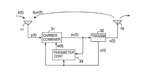
In Fig. 3 there is illustrated the basic configuration of
the present invention. Assume that every signal mentioned
below is represented by a complex envelope. That is, a
signal of a real number is represented by a complex envelope
x(t) such as xr(t)=Re~x(t)exp(j2nft)}. A carrier combining
section 31 combines a received signal y(t) and a canceling
signal u(t) and derives a combined base band signal y~(t) from
the combined signal as a complex envelope signal. The both
signals may be combined in any stages of the radio frequency
band, the intermediate frequency band and the base band, or
in a desired combination of such frequency bands.
A transmitting section 32 generates a send signal and a
erI ~~~~~ll~g ~Zgnal through u~lli~~~iQ~ Qt ~ ~~~~ ~Zg~~l ~h~~,~~~
obtained by demodulating the combined base band signal. The
canceling signal is generated from a signal in a desired
stage from the generation of a base band signal ub(t) by re-
modulating the demodulated version of the received signal to
the generation of a radio frequency signal ur(t). Since the
CA 02208842 2000-02-29
-7-
send signal is produced merely by multiplying the canceling
signal by a certain complex number, the send signal and the
canceling signal will hereinafter be represented by u(t). A
parameter control section 33 calculates a cancel parameter
w(t) from the combined base band signal and the canceling
signal and outputs it to the carrier combining section.
A detailed description will be given of the operation of
each section. As referred to above, a real number signal
will be represented by the complex envelope x(t) like xr
(t)=Re{x(t)exp(j2nft)}. Accordingly, the real part Re{x(t)}
represents the amplitude of an in-phase component and the
imaginary part Im{x(t)} the amplitude of the quadrature
component. The carrier frequency f will be represented by fr
in the RF band (the radio frequency band), fIF in the IF band
(the intermediate frequency band) and 0 in the base band.
The description with the complex envelope allows ease in
representing similar processing in the RF band, the IF band
and the base band.
Superimposed on the received signal complex envelope y(t)
received by a receiving antenna 11 are a desired wave complex
envelope s(t), an interference wave complex envelope qou(t)
that is a leakage of a send signal complex envelope u(t)
emitted from a transmitting antenna 18 and received by the
receiving antenna, and a noise complex envelope n(t). The
signal complex envelope y(t) is expressed by the following
equation:
y(t) - s(t)+qau(t)+n(t) (1)
CA 02208842 1997-06-26
w
-g-
where qo is a complex coupling coefficient between the
transmitting and receiving antennas 11 and 18. The send
signal u(t) is produced by delaying a demodulated signal for
a time id, then modulating it again to obtain a signal s(t-
id), and amplifying it by a complex gain G with respect to the
input level. The send signal is expressed by the following
equation:
u(t) - Gs (t-~;d)
(2)
The carrier combining section 31 multiplies the canceling
signal u(t) by tree cancel parameter w(t) to generate a
replica signal complex envelope r(t)=w(t)u(t) and utilizes
the difference between the received signal y(t) and the
replica signal r(t) to generate a combined signal complex
envelope yo(t).
~ yo(t) - y(t)-r(t) - y(t)-w(t)u(t) (3)
As described later on with reference to Fig. 4, the
carrier combining section 31 further processes the combined
signal yo(t) by amplification, frequency conversion and band-
pass filtering and outputs it as the combined base band
signal y~(t). The combined base band signal y~(t) thus
produced by amplification, frequency conversion and band-pass
filtering is the came as a signal that is obtained by
multiplying the combined signal yo(t) by a certain complex.
The combined base band signal y~(t) is produced by the IQ
detection of the <:ombined signal yo(t), that is, by
multiplying the input modulated signal by in-phase and
quadrature carriez: signals and eliminating harmonic
, CA 02208842 1997-06-26
K
-9-
components with a low-pass filter, and the real part Re~y~(t)}
and the imaginary part Imfy~(t)} are output as two base band
signals. These signals will hereinafter be identified intact
by the complex number y~(t). Incidentally, the combined
signals yo(t) in the RF band, the IF band and the base band
differ in magnitude and in phase, but since their variations
are each a merely fixed multiple of the complex number, they
will be identified by ye(t)=yo(t) in common to them for the
sake of simplicity.
In the present invention, the interference signal may be
canceled in the IZF' band, in the IF band, in the base band, or
in an arbitrary r_ombination thereof. In the case of
canceling the interference signal in the base band, the
canceling signal u(t) in the base band is multiplied by the
cancel parameter w(t) to generate the replica signal r(t)=w
(t)u(t) in the base band and the difference between the
received signal y(t) and the replica signal r(t) is used to
directly generate the combined base band signal y~(t) by Eq.
(3).
The combined base band signal y~(t) from the carrier
combining section 31 is demodulated in the transmitting
section 32 to obtain a demodulated data signal, which is
again subjected to demodulation similar to that of the
received signal, by which a send signal ur(t)=s(t-id) is
generated. The send signal s(t-id) is a radio wave of exactly
the same type as the signal transmitted from the base station
and a pilot signal is not superimposed on the send signal nor
CA 02208842 2000-02-29
-10-
is its carrier modulated. The send signal s(t-id) is
transmitted from the transmitting antenna 18, while at the
same time the canceling signal u(t) is generated from the
send signal and fed to the carrier combining section 31. In
the parameter control section 33 the parameter w(t) is
controlled to be optimum so that the component of the send
signal s(t--cd) is not contained in the combined base band
s ignal y~ ( t ) .
A variety of methods can be used to calculate the
parameter in the parameter control section 33 of the above
booster system. A concrete example will be described below.
Assuming that the coupling coefficient qa between the
transmitting and receiving antennas 18 and 11 does not
fluctuate, the cancel parameter w(t) naturally ought to
remain unchanged and hence it will be identified by w(t)=w.
The power of the combined base band signal y~(t) is the sum of
the powers of a desired wave, an interference wave and noise
when the interference wave is left unremoved. As the
interference wave is removed using the replica signal r(t),
the power of the combined base band signal y~(t) gradually
decreases and when the interference wave is completely
removed, the power of the combined signal y~(t) is minimum.
Hence, in the case of using the power of the combined base
band signal y~(t) as an evaluation function J, control
expressed by the following equation is effected:
J = IY~(t)IZ
<,J> _ < I y ( t ) -wu ( t ) I 2> --~ minimum power ( 4 )
CA 02208842 2000-02-29
-11-
where ~z~ represents the absolute value of z and <> a set
mean, which is a time mean in practice. The interference
cancellation can be performed in any of the RF band, the IF
band and the base band. Letting the cancellation in all of
the three bands by y(t)-wu(t) and setting y(t)=s(t)+qou(t)+n
(t), the evaluation function ,7 can be modified as follows:
<J> _ <~s(t)+qou(t~~+n(t)-wu(t) (2>
- <~S(t) ~Z>+<~qo-w~z~u(t) ~Z'~'~~n(t) ~2>
+2Re[<s*(t)(qo-w)u(t)>+<s*(t)n(t)+<qo-w)u*(t)n(t)>1
(5-1)
where a9==< ~ s ( t ) ~ Z>; ~z=< ~ a ( t ) ~ 2> and Qn2=< ~ n ( t ) ( 2> and
A*
represents a complex conjugate of A. Since noise is utterly
random and has no correlation with the signals s(t) and u(t),
<s*(t)n(t)>=0 and <u*(t)n(t)>=0.
Further, set <s*(t)u(t)>=asor"p, where p is a correlation
coefficient between the signals s(t) and u(t). By such
setting, Eq. (5-1) becomes as follows:
<J> = as2+ ~ qo-w ~ 2~2+~2+2as~ ( qo-w ) Re [ P J ( 5-2 )
Since the received signal is modulated after being
demodulated, the delay time ~ from the reception of the
received signal to the generation of the modulated signal
after the demodulation is sufficiently longer than the symbol
period T9.and the delay time id can be regarded to be much
greater than T9. In this instance, the signals S*(t) and u(t)
at time t are modulated differently, and since a mean value
of their product, <S*(~t)u(t)>, is substantially zero, the
correlation coefficient p can be regarded to be approximately
CA 02208842 1997-06-26
-12-
equal to zero. Hence, Eq. (5-2) becomes as follows:
<J> = 6S2+6n2+ I qo-w ~ 2~u2 (
As will be seen from the above equation, under the
condition that the interference can completely be canceled,
that is, when w=qo, the evaluation function J is minimized.
In practice, howEwer, since the value of the coupling
coefficient qo is unknown, it is necessary to calculate its
value by one algorithm or another. Now, let w at the sample
point kTs be represented by w(k), omitting TS, and consider
iterative updating of the parameter w(k) by the steepest
descent method (s.Haykin, Adaptive Filter theory, 2nd
edition, Prentice-Hall, 1991) as follows:
w(k) - w(k-1)-(u/2)aJ/aw~t = kT (7)
where a is a step size. Partial differentiation of Eq. (4)
gives
8J/c~w = -2y(t)u*(t)+2u(t)u*(t)w = -2y~(t)u*(t) (8)
(see the above-mentioned literature). Substitution of this
into Eq. (7) gives such an algorithm as follows:
W(k) - w(k-1)+uY~(k)u*(k) (9)
As described above, the coefficient can be updated by
multiplying the combined base band signal y~(t) by the
conjugate complex number of the complex envelope of the
canceling signal u(t) and the step size fir. In other words,
uY~(k)u(k) is fed back to the preceding cancel parameter w(k-
1), by which the cancel parameter is updated.
Fig. 4 illustrates in more detail an embodiment of the
carrier combining section 31, in which signals are combined
CA 02208842 1997-06-26
1
-13-
in each of the RF stage, the IF stage and the base band stage
for cancellation of the interference signal. Three canceling
signals ur(t), u~(t) and ub(t) are input from the transmitting
section 32 in Fig. 3 (described later on with reference to
Fig. 5) into the RF band, IF band and the base band stages,
respectively. The parameter control section 33 (Fig. 3) is
supplied with the base band combined signal y~(t) and the
canceling signals ur(t), ui(t) and ub(t) from the transmitting
section in Fig. 5 and creates cancel parameters wr(k), wi(k)
and wb(k) for the RF band, the IF band and the base band,
respectively, by the following equations:
wz.(k) - wr(k-1)+urYa(k)ur*(k) (10)
wi(k) _ wi.(k-'1)+uiYc(k)ui*(k) (11)
wb(k) _ wb(k_.1)+l~bYc(k)ub*(k) (12)
where ur, u1 and ub represent correcting step sizes in the RF
band, the IF band and the base band, respectively.
An RF complex envelope converter 35, made up of two
multipliers and a rr/2 phase shifter, complex-multiplies the
RF canceling signal ur(t) by the parameter wr to generate an
RF-band replica signal rr(t). Similarly, an IF complex
envelope converter 36, formed by two multipliers and a rc/2
phase shifter, generates an IF-band replica signal ri(t), and
a base band complex multiplier 37 complex-multiplies the
canceling signal ub(t) and the parameter wt to generate a
base-band replica signal rb(t).
In a combines 38 the received signal y(t) from the
receiving antenna 11 and the replica signal rr(t) are
CA 02208842 1997-06-26
-14-
combined, that is, the replica signal rr(t) is subtracted from
the received signal y(t), thereby obtaining a composite
signal yor(t) processed for interference cancellation in the
RF band. The signal yor(t) is amplified by a low noise
amplifier 39. The amplified output is fed to a frequency
converter 42, wherein it is converted to an IF band signal by
a local signal o:E a frequency fL from a local oscillator 41,
then the converted output is filtered by a band-pass filter
43 and combined with the replica signal rift) in a combiner
44, that is, the replica signal rift) is subtracted from the
filtered output, whereby the residual component of the
interference signal in the IF band is canceled. The combined
signal yor(t) processed for interference cancellation in the
IF band is amplified by an AGC amplifier 45 and then fed to
an IQ detector (a quadrature detector) 46, wherein the
amplitudes of its in-phase and quadrature components are
extracted. The quadrature detected output signal and the
replica signal rb(t) are fed to a combiner 47, wherein the
latter is subtracted from the former and from which a
combined signal y~b(t) processed for interference cancellation
in the base band is output as the combined base band signal
Y~(t)-
By canceling the interference wave in three steps as
described above, an optimum amount of cancellation can be set
in hardware in each stage--this provides a merit that
excessively high accuracy is not required in each section.
In Fig. 3, the power level of the signal qou(t) that leaks
CA 02208842 2000-02-29
-15-
from the transmitting antenna 18 to the receiving antenna 11
is usually about 30 to 40 dB higher than the power level of
the desired signal s(t) at the receiving antenna 11, so that
the interference cancellation processing by the RF-band
combiner 38 using the RF-band replica signal r=(t) enables the
maximum gain for the desired signal to be increased within
the range over which the operation of the low noise amplifier
39 remains unsaturated. Resides, when the signal processing
by the complex multiplier 37, the quadrature detector 46 and
the combiner 47 in the base band is performed as digital
processing, processing accuracy can be increased as compared
with that of analog processing.
Fig. 5 illustrates in detail an embodiment of the
transmitting section 32 in Fig. 3. The combined base band
signal yob(t) or y~(t) in Fig. 4 is demodulated by a
demodulator 51 into a data signal and a modulation is carried
out again based on the data signal. This modulation is
performed in two steps. In the first place, a base band
modulated wave complex envelope (a base band modulated
signal) ub(t) is generated by a modulator 52 using the data
signal sequence, then this signal is fed to a quadrature
modulator 53 composed of two multiplier, a n/2 phase shifter
and an adder, wherein it is frequency converted by a local
signal fIF from a local oscillator 54 into an
IF-band modulated signal. The IF-band modulated signal ui(t)
thus obtained is fed to a frequency converter 55, wherein it
is further frequency converted by a local signal from a local
CA 02208842 1997-06-26
-16-
oscillator 56 to an RF band signal, and the frequency
converted signal is output as the send signal ur(t) via a
band-pass filter 57 and the transmitting amplifier 15. The
output from the modulator 52 is provided as the base-band
canceling signal ub(t) to the multiplier 37 in Fig. 4, the
output from the quadrature modulator 53 as the IF-band
canceling signal ui(t) to the complex envelope converter 36
and the send signal ur(t) as the RF-band canceling signal
ur(t) to the complex envelope converter 35 from the coupler
19.
In the Fig. ~4 configuration the IF amplifier (the AGC
amplifier) 45 is used as a level detector. More
specifically, the output from a logarithmic amplifier serving
as the level detector 45 or a gain control signal of an
automatic gain control amplifier as the level detector 45 can
be used as a level signal. The observation of a mean level
by such a level detector permits calculation of the cancel
parameters as described below.
When interference has not ever been canceled, the level
is the combined power of the desired wave, the interference
wave, noise and the replica as indicated by Eq. (6). By
adjusting the amplitude and phase of the replica so that it
cancels the interference wave with each other, the composite
level ought to drop. When the interference wave is canceled
with the highest degree of accuracy, the output from the
level detector 45 indicates the combined power level of the
desired wave and noise and the power is minimum. Therefore,
CA 02208842 1997-06-26
-17-
it is also possible to control the parameters wr and wi to
minimize the detected level of the level detector 45 while
observing the level. The parameters for adjusting the
amplitude and phase are iteratively calculated by trial and
error. However, this method is effective in the cancellation
only in the RF band and the IF band since the cancellation
must be done before processing proceeds to the level detector
45. Furthermore, no phase information is available and only
the level is utilized for adjustment, so that there are Cases
where accuracy is not so high. Hence, this method is
suitable to coarse adjustment. The parameter wb is adjusted
using Eq. (9).
Fig. 6 illustrates a modified form of the transmitting
section 32, in which an attenuator 58 is provided as a level
controller to control the transmission output. Immediately
after the start of operation of the booster system the cancel
parameters wr, wi and wb do not yet converge to optimum values
and a signal from which the interference wave has not
sufficiently been removed is input into the demodulator 51.
As a result, the demodulated data becomes completely random
and the send signal is also modulated completely randomly.
To avoid this, the output is held at a level at which the
desired wave can be demodulated satisfactorily even if the
interference wave is not canceled at the beginning and the
output is gradual7_y increased to such an extent that the
cancel parameters can be obtained. The attenuator 58 is
placed under the control of the parameter control section 33.
CA 02208842 1997-06-26
-18-
The receiving circuit of Fig. 4 and the transmitting
circuit of Fig_ 5 use many local oscillators. If thP;r
frequency accuracy is low, the phase of the complex envelope
of the interference component, when observed in the base
band, rotates with respect to the desired wave by a frequency
setting error for each local oscillator. When the cancel
parameters sufficiently follow the phase rotation, the
interference can be canceled, but in practice, a steady phase
error inevitably occurs due to the follow, deteriorating the
parameter estimation accuracy. To avoid this, these local
oscillators are synchronized by a phase lock loop with the
output phase of one reference oscillator, by which the phases
of the local oscillator outputs as well as their frequencies
are synchronized.. With the use of this method, the parameter
control section 33 needs not to follow the phase rotation of
the interference wave, so that the cancel parameters can be
obtained with high accuracy.
The above description has been given on the assumption
that the approximation pC0 holds in Eq. (5-2). To implement
this,' it is necessary that id»TS and that <s*(t)u(t)>=<s
*(t)s(t-id)>C0. When the desired wave signal has its spectrum
limited in a narrow band, long inter-symbol interference
occurs with respect to the symbol period Ts, incurring the
possibility of preventing the above-said approximation from
holding. This problem can be overcome by setting the carrier
frequency of the send signal u(t) slightly off the carrier
frequency of the received desired wave signal s(t). Now, let
, CA 02208842 1997-06-26
-19-
fr represent the carrier frequency of the received wave from
the base station that is the desired wave s(t) for the
booster system and fr' the sending carrier frequency of the
booster system. The send signal u(t) can be expressed by the
following equation using the send signal uo(t) in the case of
no frequency offset being provided:
u(t) - ua(t)exp(j2n~ft) (13)
~f = fr'-fr (14)
When ~f=0, u(t) becomes ua(t). The frequency offset Of is
chosen such that the signal spectrum of the send signal u(t)
falls within a px-edetermined band. By this, even if the
requirement for Fq. (6), <s*(t)uo(t)>C0, is not satisfied,
that is, even if the correlation between the signals s(t) and
uo(t) becomes zero, a mean of exp(j2n~ft) becomes zero after
the elapse of time sufficiently longer than a time constant
1/df, and the following equation can be made zero.
p = <s*(t)uo(t)exp(j2naft)>/(asau) (15)
This method provides a slight frequency offset of and can
hold it within a permissible range as an ordinary in-band
frequency drift. Hence, this method does not so much disturb
the signal as in the case of the second-mentioned
conventional method (Fig. 2).
A concrete method is to provide the frequency offset in
the modulator 52 :in Fig. 5. The modulator 52 outputs the in-
phase and quadrature components of the signal u(t) as the
base band signal. That is, the modulator outputs the signal
u(t) as ub(t). Since the base band signal s(t-id) is output
CA 02208842 2000-02-29
-20-
when no frequency offset. is provided, the signal ub(t) at this
time will be identified as u~ ( t ) . That is , u~=s ( t-id ) . The
frequency offset can easily be obtained through complex
multiplication of u~(t) by exp(j2rrpft) in the modulator. At
this time, ub ( t ) =u~ ( t ) exp ( j 2rrOft ) . The modulator, which
provides the frequency offset, outputs the in-phase and
quadrature components of the signal ub(t)=u~(t)exp(j2rrAft) as
the base band signal ub(t). Since the signal ub(t) thus
generated has the frequency offset ~f, the replica signals
ub(t), ui(t) and ur(t) in Fig. 5 also contain the offset.
.. Since the thus frequency-offset send' wave ur(t) leaks to the
receiving antenna, the leakage signal can be canceled by the
offset replica signals. Therefore, the description from Eqs.
(4) through (12) holds true as it is.
Another method is to offset the oscillation frequency fIF
or fL of the local oscillator 54 or 56 in Fig. 5 by df. These
oscillators are synchronized with the local oscillators 41
and 48 at the receiving side (Fig. 4) as described
previously, and an accurate frequency offset ~f can be
obtained by offsetting the frequencies of the former while
maintaining their phase synchronization with the latter. Let
it be assumed that the frequency offset ~f is provided to the
local oscillator 54. In this case, since the signals ui(t)
and ur(t) are also merely offset by Af, the cancel algorithm
is the same as the afore-mentioned. Since no offset is
provided for the signal ub(t), it is regarded as the signal
u~(t) and its complex-multiplied version ub(t)=u~(t)exp
CA 02208842 1997-06-26
-21-
(j2noft) is input into the complex multiplier 37 in Fig. 4.
Alternatively, the signal u~(t) is input intact into the
complex multiplier 37 and wbexp(j2nOft) obtained by
multiplying the cancel parameter wb by exp(j2nAft) is fed to
the complex multiplier 37--this also produces the same effect
as mentioned above.
In the above the coupling coefficient qo between the
transmitting and receiving antennas of the booster system has
been described to be constant. In practice, however, the
coefficient qo is considered to vary with a change in the
surrounding environment such as a temperature change. If
this change is gesntle, the algorithm of Eq.(9) ought to
adaptively follow the change in the coefficient qo. The
following rate can be adjusted using the step size a (ur, ui~
ub). Theoretical.ly, 1/u is a time constant of this algorithm,
which increases with a decrease in the step size u, and
highly accurate interference cancellation can be achieved
using a long time mean. On the other hand, an increase in
the step size a causes a decrease in the time constant and
the algorithm quickly follows the coefficient fluctuation.
In general, t:he cancel sections in the RF band and the IF
band use analog circuits as their components, and hence they
are not so high in accuracy. On the other hand, the cancel
section in the base band performs digital signal processing,
and hence it is highly accurate and capable of fine control.
With the cancellation in the base band, however, saturation
of the low noise amplifier or the like cannot be deal with.
CA 02208842 1997-06-26
-22-
For this reason, it is desirable to perform each cancellation
in correspondence with one component of q. The coupling
coefficient is considered to be separated such that q=qo+pq,
where qo is a ger.~tle variation component as mentioned above
and ~q a relatively quick variation component. In general,
it is considered that qo is much greater than dq in many
cases. Hence, in the cancellation in the RF~and IF bands the
step size ur or ui in Eq. (10) or (11) is chosen relatively
small. This cancels the gently varying components of tight
coupling. The step size ub is chosen relatively large for the
purpose of canceling the residual component and the rapidly
varying component by the base band canceler. The base band
cancellation is carried out by digital signal processing, and
hence it is highly accurate. Furthermore, an RLS algorithm
and Kalman filter known as excellent adaptive signal
processing, other than Eq. (12), can be employed according to
the rate of fluctuations.
EFFECT OF THE INVENTION
As described above, the present invention cancels the
interference component without involving the insertion of a
pilot signal and modulation, and hence it does not ever
disturb the transmission wave and has significantly excellent
interference cancellation performance because of adaptive
signal processing in the base band. The present invention is
of great utility when employed in mobile communication,
especially in the booster system of the radio paging system.