Note: Descriptions are shown in the official language in which they were submitted.
CA 02208845 1997-06-26
W O 96J21892
PCT/GB96/00033
1
ELECTRICAL APPARATUS
BACKGROUND OF THE INVENTION
FIELD OF THE INVENTION
The present invention relates to an item of
electrical apparatus, and in particular to apparatus for
converting the supply voltage of a DC power supply.
SUMMARY OF THE PRIOR ART
Recent years have seen the emergence and
development of a wide range of electronic accessories for
motor vehicles, motor boats and other large pieces of
equipment. Among such electrical accessories are lights,
heating units, and more recently of course increasingly
sophisticated telecommunications devices. Rather than
carry their own source of electrical power, many
accessories are intended to draw energy from the battery
power source of the larger pieces of equipment, and are
therefore designed to be compatible with the 12 volt
batteries which are now standard in motor cars. The
optimum input voltage of many electronic accessories is
in fact 13.8 volts.
Unfortunately, the DC supply format used in other
industrial, military, commercial, aviation, maritime and
CA 02208845 1997-06-26
WO 96121892
2
PCT/GB96/00033
other applications differs considerably. Large
vehicles, for example, require electrical power to be
carried over comparatively longer lengths of cable with,
Y
in addition, an increased number of devices using the DC
supply.
Therefore, if the DC supply is doubled in voltage
from the nominal 12 volts to a nominal 24 volts the
current demand is halved although the overall power
available would be unchanged.
For example, large commercial or heavy vehicles
typically use the higher DC voltage format centred around
a nominal 24 volts.
There is therefore a requirement for converters
capable of receiving the output of.these higher DC
voltage formats and supplying current in an acceptable
form to 12 volt format electric accessories, that is to
say a converter capable for example, of providing a
constant supply of 13.8 volts from a varying supply of
between 23.3 volts and 27.6 volts.
It should be appreciated that such a converter
may have to deliver a power supply of several watts, tens
of watts or even hundreds of watts, and that in this
context problems are encountered which have no
CA 02208845 1997-06-26
WO 96121892
PCT/GB96/00033
3
counterpart in microelectronic power conversion systems.
For example, US-A-4827205 discloses anon-chip 10 volt
voltage supply in which current is delivered through a
lOk resistor, which limits the power delivery to be of
the order of milli-watts. In such a context conversion
efficiency is unimportant and heat generation causes no
significant problems.
An early generation of DC power converters, often
misnamed "Droppers", were based upon linear converters,
which is to say devices which step-down and regulate a
voltage supply principally using transistor technology.
It was perceived, however, that such devices perform
their tasks with unacceptably low power conversion
efficiency. Furthermore, no design of linear converter
was found which could provide an output voltage with
sufficient stability, particularly when the current
demand at the output increased to any significant degree.
Many devices used as accessories in vehicles,
boats, the aviation industry or other equipment; require
a reasonably smooth and stable DC supply voltage.
Recent developments in DC power converters have
therefore concentrated on methods of DC power conversion
in which a DC supply powers an oscillator circuit, often
CA 02208845 1997-06-26
WO 96/21892
PCT/GB96/00033
4
housed under the dashboard of the iorry,.for generating
an oscillating voltage across the terminals of a step-
down transformer. The output of the transformer is then
rectified, smoothed and regulated to provide the desired
supply, usually nominally 12 volts. Surprisingly,
progressive refinements of this method-have resulted in
devices of up to 75o efficiency, and such systems are
very widely employed.
The present inventor has found, however, that
oscillation based power converters suffer from at least
two serious disadvantages.
A first disadvantage of many switched-mode
(oscillation) based converters is that their circuitry is
all too likely to be damaged by the heat generated within
them when the converter is abused, for example by direct
electrical connection of its output terminals. In
practice over the life of the converters operatives tend
to replace any safety fuses. (or fuses supplied with the
converter) with incorrect fuses or, worse, by-pass them
entirely. '
This leads to significant fire hazards.
Secondly, they generate by their nature powerful
electromagnetic radiation, often referred to as radio
CA 02208845 1997-06-26
WO 96!21892 PCT/GB96/00033
frequency interference, which is often radiated in a
manner that affects electrical, electronic and more often
communications equipment within the local area of the
converter.
5 This is a widespread occurrence and, although
many devices are claimed to have adequate filtering
within their design, this problem occurs continually.
This problem is potentially more serious when the
radiation affects users of devices and/or communications
equipment completely remote and both unattached and
unconnected to the converter mounted on the vehicle or
equipment in question.
In many instances the user of the conversion
device has no knowledge that it may be causing
interference externally to other services.
SUMMARY OF THE INVENTION
The present invention, which is intended, inter
alia for use in private, commercial and military
vehicles, private, military and commercial maritime craft
or smaller boats, the aviation industry, industry
generally and for other pieces of equipment, seeks to
overcome the problems of electromagnetic radiation and/or
of overload conditions whatever external protection may
CA 02208845 2003-O1-07
a
WO 9612!892 . PCTIGB96/00033
6
exist with respect to relevant fuse ratings.
In its most general terms, the present invention
proposes a converter having a first portion which
controls DC voltage conversion and a second portion,
spaced from the first, in which heat may safely be
developed.
A first aspect of the invention provides a DC
power converter comprising at least two input terminals
having a DC input voltage supplied thereto: an input
resistance electrically connected to at least one.of the
input terminals and a DC regulating circuit, electrically
connected to the input resistance and to another of the
input terminals, such that the DC regulating circuit and
the input resistance are connected in series and receive
the DC input voltage. The DC regulating circuit has at
least one output terminal which is electrically
connectable to an external load, whereby the DC
regulating circuit can transmit at least several watts of
power to the external load in the form of a DC output
voltage lower than the DC input voltage. The input
resistance and the DC regulating circuit are housed in
first and second separate heat dissipative housings. The
first housing is adapted to dissipate heat generated by
the input resistance and the second housing is adapted to
CA 02208845 2003-O1-07
~ ~ WO 96!21892 PCT'IGB96100033
6a
dissipate heat generated by the DC regulating circuit.
The DC regulating circuit ceases to supply an output
voltage when at least a portion of the regulating circuit
is at a temperature above a predetermined value.
A further aspect of the invention provides a DC
power converter for mounting to a vehicle and comprising
at least two input terminals having a DC input voltage
supplied thereto, an input resistance electrically
connected to at least one of said input terminals and a
DC regulating circuit, electrically connected to said
input resistance and to another of the input terminals,
such that the DC regulating circuit and the input
resistance are connected in series and receive the DC
input voltage. The DC regulating circuit has at least
one output terminal which is electrically connectable to
an external load, whereby the DC regulating circuit can
transmit at least several watts of power to the external
load in the form of a DC output voltage lower than the DC
input voltage. The input resistance and the DC
regulating circuit are housed in first and second
separate housings and are connected by at least one
cable, whereby the housings may be located at
CA 02208845 2003-O1-07
WO 96!21892 PCTIGB96100033
7
predetermined different distances from each other on the
vehicle. At least the first housing is adapted to
dissipate heat generated by the input resistance by at
least thermal conduction to the vehicle.
A converter according to the
present invention is preferably capable of delivering
electrical power of at least one watt, and more
preferably electrical power up to several tens or
hundreds of watts.
The resistor of the input resistance means will
usually have a value not greater than 10 ohms, preferably
0.1 to S ohms and most preferably 0.5 to 1.5 ohms.
It is intended that in use the converter is
connected to the battery power supply of a large piece of
equipment, for example a lorry, and that the resistance
means is mounted on the body of the equipment, e.g. the
chassis of the lorry, so that heat may be dissipated to
the body distant from the regulating circuit.
- Although the regulating circuit nay use
oscillation it preferably employs linear converters, so
that substantially no electrical noise is created on the
output power supply. In this case both the disadvantages
CA 02208845 1997-06-26
WO 96121892 PCT/GB96/00033
8
of linear converters described above may be overcome, or
at least substantially reduced, since the regulating
circuit can be selected so that in use a major portion,
for example at least 60a and preferably at least 70% of '
the heat generated by the voltage converter is produced
in the resistance means, and be spaced distant from the
regulating circuit. This arrangement significantly
lessens the necessity for the circuit to perform power
conversion at high efficiency, since there is less heat
generation in the location of the regulating circuit
itself, and hence the regulating circuit can be selected
to optimise output stability and regulation regardless of
the output current drawn. Overall power conversion
efficiency is not of paramount importance in this
application, since both the supply current capability and
the battery capacity are very large in the application
specified.
The regulating circuit is preferably further
selected to limit the current which can be drawn from the
converter, for exampl= ~?y ~-=mltirig t'~= output current to
be below an upper critical limit, or simply by ceasing to
supply output voltage when the converter detects an
irregularity in the current drawn from the converter, a
CA 02208845 1997-06-26
W O 96/21892 PCT/GB96/00033
9
technique known as fold back. This is preferably
achieved independently of the presence or absence of
interrupters such as fuses or circuit breakers, which can
be tampered with.
The resistance means is preferably adapted for
mounting on the body of a large piece of machinery in
such a way that there is good heat conduction
therebetween, whereby heat generated within the
resistance means is rapidly conducted away. The
regulating circuit is preferably mounted on a heatsink
formed with a high surface area to enhance its capacity
to transmit heat generated by the regulating circuit to
ambient air, e.g. by convection.
The heatsink for use with the regulating circuit
preferably has high surface area and longitudinal
symmetry. It may be mounted with its longitudinal axis
vertical so that when it becomes warm a vertical flow of
air is created along it, thereby improving the ability of
the heatsink to transmit to the atmosphere the heal
generated by the regulating circuit.
The regulating circuit is preferably selected to
cease transmitting power when the temperature of the
circuit rises above a predetermined value. This "thermal
CA 02208845 1997-06-26
WO 96/21892 PCT/GB96/00033
cutout" is a useful safety feature, even in combination
with the fold back feature described above, since the
conditions which trigger fold back do not necessarily
occur instantaneously upon occurrence of a fault. "
5 Furthermore, it is possible to have overheating without
electrical overload, for example if theregulating
circuit is located in a region too warm for the heat sink
to operate satisfactorily.
BRIEF DESCRIPTION OF THE DRAWINGS
10 Further objects and advantages of the present
invention will be explained in the following detailed
description of preferred exemplary embodiments with
reference to the accompanying figures in which:-
Fig. 1 shows the circuit diagram of a first
embodiment of a DC converter according to the invention;
Fig. 2 shows the circuit diagram of a second
embodiment of the DC converter;
Fig. 3 shows a circuit diagram of a third
embodiment of the DC converter;
Fig. 4 shows a circuit diagram of a fourth
embodiment of the DC converter;
Fig. 5 shows a circuit diagram of a ffifth
embodiment of the DC converter;
CA 02208845 1997-06-26
WO 96/21892 PCT/GB96/00033
11
Fig. 6 illustrates the relationship between the
temperature of the heatsink of the third and fifth
embodiments of the DC converter with the output current
supplied;
Fig. 7 is an end view of a heat sink suitable for
use in the present invention;
Fig. 8 ,is a cross-sectional view of a regulating
circuit according to the present invention incorporated
into the heat sink shown in Fig. 7;
Fig. 9 shows a perspective view of the heat sink
of Fig . 7 ;
Fig. 10 shows a perspective view of a resistance
unit for use in a converter according to the present
invention; and
Fig. 11 illustrates the installation of a DC
converter according to the invention.
DETAILED DESCRIPTION
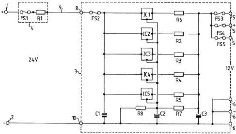
Referring firstly to Fig. 1, the first embodiment
of the DC converter of the present invention has input
terminals 1,2 for connection respectively to the
terminals of an external battery ofa piece of equipment,
such as the 24V battery of a lorry. The regulating
circuit is positioned within a regulating unit 3 which
CA 02208845 1997-06-26
WO 96/21892 PCT/GB96/00033
12
has input terminals 8,10 for receiving -electrical power
and output terminals 5,6 for connectionto the power ,
inputs of electronic accessories. The converter steps
down the DC voltage from the battery so that the voltage
S difference between its input terminals 1,2 is greater
than e.g. twice the voltage difference between the output
terminals 5,6. In series with the regulating unit 3
between the battery terminals 1,2 is resistance unit 4
comprising a resistor R1 and a fuse FS 1.
The resistance unit 4 is connected to the
regulating unit 3 by a cable 9, the length of which is at
least several centimetres and preferably up to several
metres, so that the resistance unit 4 can be located
distant from the regulating unit. The resistance unit 4
is adapted to be mounted on a massive part of the
equipment such as the chassis of the lorry, so that the
heat it generates is transmitted into the chassis. The
regulating unit 3 is located elsewhere on the lorry,
either at a different location on the chassis or, for
example, under the lorry dashboard, and makes good
thermal contact with a heatsink adapted to transmit the
heat generated by the regulating unit 3 to the
surrounding air.
CA 02208845 1997-06-26
WO 96/21892 PCT/GB96/00033
13
Within the regulating unit 3, current is divided
equally between the resistors R2, R3, R4, R5 and R6, all
of equal resistance, of the same order as (but not
necessarily the same as) the resistance of R1. The
voltage between output terminals 5 and 6 is maintained at
12 volts using 5 regulators IC 1 to IC 5 which each have
a 3 amp specification, and are controlled in operation by
resistors R7 and R8 and capacitors C1, C2 and C3. In
this way using standard components it is possible to
maintain an output current of up to 15 amps, which is
considerably higher thanthe current output of
conventional converters.
The regulators IC1 and IC5 are preferably
selected so that the regulating unit 3 ceases to supply
power when the regulators reach a predetermined
temperature. For example, the regulators may be
integrated circuits KA350, which has that property.
In one selection of component values which gives
correct 24 voltage to 12 volt conversion, R1 takes the
value of .5 ohms, while resistors R2 to R6 each have a
resistance of .015 ohms; C1 is a 1,000 ~,F/35 volt
electrolytic capacitor; and C2 is a 100 ~,F/16 volt
electrolytic capacitor. IC 1 to IC 5 may be 8 volt/3 amp
CA 02208845 1997-06-26
WO 96/21892 PCT/GB96/00033
14
regulators and in this case resistors R7 and R8 have
values of 220 ohms and 150 ohms respectively.
Alternatively, IC 1 to IC 5 may be 5 volts/3 amp
regulators and in this case R7 and R8 have values of 500
and 860 ohms respectively. In alternative embodiments,
the regulators IC 1 to IC 5 are 12 volt regulators, and
the voltage of the output ofthe circuit can be made to
be 13.8 volts by selecting R7 and R8 to be 480 and 72
ohms respectively. C3 is a 2200 ~.F/16 volt electrolytic
capacitor.
In this embodiment FS 1 and FS 2 are blade fuses
having respectively 25 amp and 15 amp capacities. FS 3,
FS 4 and FS 5 are a further three blade fuses, the total
value of which does not exceed 15 amps; usually each has
a capacity of 5 amps.
Fig. 2 illustrates a second embodiment of the
invention being a modified version of the first
embodiment. This second embodiment is preferred to the
first embodiment, since it is cheaper and simpler to
manufacture. It is designed to output 5 amps, and will
automatically cease supplying power in conditions of
electrical overload or overheating. The converter will
then automatically recommence normal functioning when the
CA 02208845 1997-06-26
W O 96121892 PCT/GB96/00033
fault condition has been removed or the temperature
reduced to a permissible level.
In this embodiment the resistance unit 4 on the
input side is separated from the regulator unit 3 by a
5 multi-cable lead 9' including connector jack and plug
assembly 9".
Values for the components in this circuit are:
IC 6, 1C 7 = Integrated circuit regulator type LM350
C 4 - Electrolytic capacitor 47~F/35V
10 C 5, C 6 - Electrolytic capacitor 100~,F/16V
D 1 - Diode IN4001
R 1' - Wirewound resistor 1.5 ohms
R 9 - Wirewound resistor 120 ohms
R 10 - Wirewound resistor 1.2K ohms
15 A third embodiment shown in Fig. 3, employs a
resistance unit 4 equivalent to that in the first
embodiment, but uses a different regulating circuit in
which current flows principally through resistor R2. The
specification of the c-omponents in the circuit is as
follows:
TR 1 - PNP Transistor (T03) MJ15004.
TR 2 - PNP Transistor (T0220) BD744.
CA 02208845 1997-06-26
WO 96/21892 PCT/GB96/00033
16
IC 8 - Integrated Circuit Regulator type L7808CP.
C 4 - Electrolytic Capacitor 2200 ~.F/16 volts.
R 1 - Wirewound Resistor, 0.5 ohm/100 watt.
R 11 - Wirewound Resistor, 0.05 ohm/25 watt.
R 12 - Metal Film Resistor 220 ohm/1 watt.
R 13 - Wirewound Resistor 3.3 ohm/2.5 watt.
R 14 - Metal Film Resistor 150 ohm/1 watt.
C 7 - Electrolytic Capacitor 1000 ~.F/35 volts.
C 8 - Electrolytic Capacitor 1 ~.F/35 volts.
C 9 - Electrolytic Capacitor 1000 ~.F/35 volts.
C 10 - Electrolytic Capacitor 2000 ~.F/16 volts.
As will be appreciated by a skilled person, the
above choice of IC8 means that the circuit ceases to
deliver a voltage when its temperature reaches a
predetermined value. Thus, there is a thermal cutout at
this temperature.
Fig. 4 illustrates a fourth embodiment of the
invention, being a modification of the third embodiment.
The fourth embodiment is preferred to the third
2.0 embodiment since it is cheaper and easier to manufacture.
CA 02208845 1997-06-26
WO 96/21892 PCT/GB96/00033
17
It is designed to output up to 15 amps.
As in the second embodiment, the regulator unit 3
is connected, via resistance unit 4, to the input and
output via a lead 9' and jack and-plug assembly 9".
Values of the components shown are:
D 2 - Diode type IN4001
IC 9 - Integrated circuit type LM 350
TR 3 - Transmitter type MJE 15004
TR 4 - Transistor type BD 744C
ZD 1 - Zener diode type IN5355B
C 11 - Electrolytic capacitor 47~.F/35V
C 12,C 13 - Electrolytic capacitor 100~.F/16V
C 14 - Electrolytic capacitor 0.47 ~.F/63V
R 1 - Wirewound Resistor 0.5 ohms
R 15 - Wirewound Resistor 120 ohms
R 16 - Wirewound Resistor 1.2K ohms
R 17a-d - Each 27 ohms
R 18 - Wirewound Resistor 0.05 ohms
In the embodiment illustrated in Fig. 5, current
is again principally conducted to output terminals 5,6
through resistor R19. The voltage is regulated using
integrated circuit IC 9, which is a regulator of type
L123CT. This converter has the feature that when the
CA 02208845 1997-06-26
WO 96121892 PCTlGB96/00033
18
circuit experiences a severe current fluctuation, which
may arise for example if the output terminals of the
circuit are connected together, IC 9 causes the output .
voltage to take a low level until itis-reset, a
S technique of current limitation known as "fold back".
Values of components in the circuit are as
follows:
TR 4 - NPN Transistor (T03) 2N3771.
TR 5' - NPN Transistor (T0220) BD743C.
IC 10 - Integrated Circuit Regulator type L123CT.
C 15 - Electrolytic Capacitor 1000 ~F/35 volts.
C 16 - Electrolytic Capacitor 10 ~.F/16 volts.
C 17 - Electrolytic Capacitor 2200 ~,F/16 volts.
C 18 - Electrolytic Capacitor 4.7 ~.F/35 volts.
C 19 - Ceramic Capacitor 470 pF/100 volts.
R 1 - Wirewound Resistor 0.5 ohm/100 watt.
R 19 - Wirewound Resistor, 0.05 ohm/25 watt.
R 20 - Metal Film Resistor 6.8 Kilohm/0.25 watt.
R 21 - Metal Film Resistor 3.6 Kilohm/0.25 watt.
R 22 - Metal Film Resistor 7.5 Kilohm/0.25 watt.
Other components have the same values as the
co rresponding
components
of
the
third
embodiment
of
the
CA 02208845 1997-06-26
WO 96121892 PCT/GB96/00033
19
voltage converter.
Fig. 6 illustrates the relationship between the
temperature of the heatsink and the current drawn from
the output of the voltage converter of Fig. 3 or Fig. 5.
The two curves represent respectively the cases that the
input to the voltage converter is 23.3 volts (the lowest
voltage typically delivered by a lorry's battery) and
27.6 volts (which may be delivered while the battery is
charging). Ideally, the converter is operated in a range
of currents between the two curves.
It has been found that the first, third and fifth
embodiments of the invention given above fulfill the
following specification.
Output Voltage . 13.8 Volts DC.
Output Current . 0 to 15 Amps.
Input Voltage . 23.3 Volts to 27.6 Volts DC.
Maximum Input
Voltage Overvolt . 35 Volts DC Short Term Fault
Condition Vehicle Supply
Current Overload
Protection . Type 2 Current Limit at 15 amps.
(Also Type 1).
Type 3 Current Foldback at 15 amps.
Operating Temperature
Range . Better than -40°C to +40°C
*At +40°C Heatsink Temperature is
CA 02208845 1997-06-26
WO 96/21892 PCT/GB96/00033
86°C/15 amps.
The second and fourth embodiments deliver up to
five and fifteen amps respectively, or a maximum wattage
of 60 or 180 Watts respectively.
5 Fig 7 is an end view of a heatsink 14 suitable
for use as the heatsink for the regulator unit. The
heatsink 14 is suitably an aluminium extrusion. It has
longitudinal symmetry, and is to be mounted with its
longitudinal axis vertical for maximum dissipation of
10 heat by convention.
Fig. 8 illustrates how the regulator circuit may
be built into the heat sink 14 shown in Fig. 7 to provide
a heat sink unit. Components 17 of the regulating
circuit, connected by a printed circuit board 19, are
15 placed in contact with a central surface 15 of the heat
sink 14, so that good thermal conduction is obtained
between the components 17 and the surface 15. The
circuit is then potted in a.thermally conductive potting
compound 21 which provides mechanical support for the
20 circuit board 1.9. The regulating circuit does not extend y
along the whole length of the heatsink-14, but leaves end
portions of the surface 15 uncovered. Thus, when the
pctting compound is applied, along the wholelength of
CA 02208845 1997-06-26
WO 96/21892 PCT/GB96/00033
21
the heatsink 14, the regulating circuit is entirely
surrounded by the potting compound except for the
portions of the components 17 which contact the heatsink
14. Thus, the regulating circuit is completely protected
-from physical interference and also from contact with any
moisture which comes into contact with the heatsink unit.
The potting compound also makes a sealing contact with
electrical leads projecting through it to the regulating
circuit, thus ensuring that moisture does not leak to the
regulating circuit in this way. Preferably, the heatsink
unit is made completely waterproof, or at least
splashproof, in this way.
An upper surface of the potting compound 21 is
covered by a plate 22. Thus the heat sink 14, and the
- plate 22 constitute a housing 25 for the regulating
circuit.
A second plate 23 closes the cavity at the other
side of the heat sink. The two plates 22, 23 are secured
together by a pin 24 with cap 25, 26. The cavity formed
between the plate 23 and the central region 15 of the
heat sink 14 is filled with a potting compound 27.
The potting compound 21, 27 used in this
embodiment is preferably thermally conductive, for
CA 02208845 1997-06-26
WO 96/21892 PCT/GB96/00033
22
example it may be a compound such as ER2/83 supplied by
Electrolube.
Fig. 9 is a perspective view of the unit shown in
Fig. 8. A bracket 30 is attached to the heat sink unit
by screws 31, 33, and is adapted for connection using
apertures 35, 37 to the body of a piece of machinery such
as under the dashboard of or to the chassis of a lorry.
Electrical inputs to the heat sink unit are via leads 38
and plug 39.
Fig. 10 illustrates in perspective view a
resistor unit 45 containing the resistor (R1,R1') of an
embodiment of a converter according to the invention.
The resistor has pins 41, 43 by which it may be
electrically connected to the rest of the converter. The
resistor unit 45 includes its resistor surrounded by, and
electrically insulated from, cylindrical portion 46 of a
housing including plates 47, 49. The housing is an
aluminium extrusion. The plates 47, 49 are provided with
apertures 51, for attaching the housing, for example, to
the chassis of a lorry,~so that excellent thermal
conduction between the resistor and the chassis is
obtained. The cylindrical portion 46 is externally
ribbed, to assist heat dissipation by convention, but
CA 02208845 1997-06-26
WO 96/21892 PCT/GB96/00033
23
typically in use between 50 and 100 watts are thermally
conducted to the chassis.
Fig. 11 illustrates the installation of a
converter according to the invention into the cab 50 of a
lorry. The heat sink unit 51 is placed, with its
longitudinal axis vertical inside the bonnet bulkhead.
The ballast resistor 53 is located in the chassis area.
The converter further comprises a fuse holder 55 inside
the cab bulkhead, a multi connector kit 57, also within
the cab bulkhead, and a LED 59 kit mounted on the
dashboard.
Many modifications to the above embodiments are
possible within the scope of the invention, as will be
clear to those skilled in the art. For example, although
preferable it is not necessary that the regulating
circuit is of the linear conversion form, and alternative
embodiments employing an oscillation-based regulating
circuit are acceptable. The converter may also be used
in combination with vehicles other than lorries, such as
marine vessels for example, or even with less
transportable items of machinery containing a DC power
source.