Note: Descriptions are shown in the official language in which they were submitted.
CA 022088~0 1997-06-26
wo s6/20s3s Pcr/sEss/0l546
DIGlTALLY COMPENSATED DIRECT CONVERSION RECEnTER
~ACKGROUND
The invention relates to a direct-conversion receiver for radio
communication systems such as portable cellular phones, cordless phones,
5 pagers, etc.
The first generation of cellular systems relied on analog frequency
modulation for speech tr~nsmiccion, and several standards have been developed,
e.g., NMT 450, NMT 900, AMPS, and ETACS.
The second generation of cellular systems, e.g., the Global System
10 for Mobile communications (GSM) in Europe, and the American Digital Cellular
System ~ADC) in North America, employ digital voice transmission and some
digital services, such as f~csimile and short message services.
Receivers in cellular systems and the other fields noted above are
preferably small, lightweight, and inexpensive. To make a portable receiver like15 a hand-held telephone smaller and less expensive, much l~sea~ch has been doneto increase the level of integration of different parts of the phone. But previous
receivers have been of the conventional heterodyne type. For applications in
small, low-cost mobile communication systems, such receivers suffer from high
production costs caused by expensive and non-integrable components, such as
20 bandpass filters.
~ To overcome such drawbacks, an alternative receiver architecture
has been developed that is based on the direct-conversion principle, in which the
frequency of the local oscillator is the same as the frequency of the received
radio carrier. Consequently, the received radio signal is down-converted directly
25 to base band in one step. Since a direct-conversion receiver does not have any
interme~i~t~ frequency (I~) stages, many filters can be omitted or simplified.
Direct conversion was introduced for single-sideband receivers in
the 1950's, but the technique is not limited to such systems. Direct conversion
can be used with many different modulation schemes and is especially well suited
CA 022088~0 1997-06-26
W096/20539 PCTISE95/01546
.
for the quadrature modulation sch~nles of today, such as minimum shift keying
(MSK) and quadrature amplitude mod~ tion (QAM). Various aspects of direct-
conversion or homodyne receivers are described in U.S. Patent Application
No. 08/303,183 entitled "Radio Receiver" by two of the current Applicants.
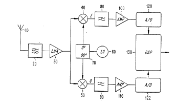
S The operation of a conventional direct conversion receiver can be
described as follows with reference to Fig. la. A radio frequency (RF) signal
having center frequency fc and bandwidth BWrf is received by an antenna 10 and
then is filtered by a bandpass filter 20. The filtered signal produced by the
bandpass filter is amplified by an amplifier 30, which preferably has low noise to
improve the total noise figure of the receiver.
The ampli~led filtered signal produced by the amplifier 30 is then
down-converted to base band in an in-phase (I) channel and a quadrature phase
(Q) channel by balanced mixers 40, 50. The mixers are driven by respective
ones of sine (I) and cosine (Q) components produced from a sinusoidal signal
generated by a local oscillator 60 by a suitable divider and phase shifter 70.
According to the direct-conversion principle, the LO signal also has the
frequency fc.
The mixers 40, 50 effectively multiply the signal from the
amplifier 30 and the I and Q components of the local oscillator. Each mixer
produces a signal that has frequencies that are the sum and difference of the
frequencies of the amplified filtered received signal and the local oscillator
signal. The difference (down-converted) signals each have a spectrum that is
folded over around zero frequency (d.c.) and that spans from d.c. to lhBWff.
The I and Q signals produced by the mixers are filtered by low-
pass filters 80, 90 that remove the sum (up-converted) signals, as well as
components that might be due to nearby R~ signals. The filters 80, 90 set the
noise bandwidth and thus the total noise power in the receiver. The I and Q baseband signals are then usually amplified by amplifiers 100, 110, and provided to
further processing components that produce the demodulated output signal. Such
CA 02208850 1997-06-26
t ~ .~
WO 96/20539 PCT/SE95/01S46
further processing can include phase demodulation, amplitude demodulation,
frequency demodulation, or hybrid demod~ tion sf,h~m~s
A major problem with the direct-conversion receiver is that
second-order products of inte,rereLs (e.g., signals on the same and nearby RF
5 communic~tion ch~nn~l~) are produced by the mixers. One component of these
second-order products is located at base band, and thus interferes with the
desired base band signal, degrading performance. In some situations, this
problem totally blocks communication in high-~e~rollllance, direct-conversion
receivers for today's time division multiple access (TDMA) digital cellular
10 systems.
For an input signal Vm, a non-linear device, such as a mixer, will
produce an output signal VO~t theoretically given by the following expression:
YO,,, = aV~" + b~ + . . .
Eq. 1
If the input signal V", is an interfering signal given by:
V"~ = V,nc~s(~ t)
Eq.2
where Vm is the inte,relel's maximal amplitude and ~c corresponds to the carrierfrequency fc, the second-order product bVm2 is given by:
b~ = ~tl + cos(2~ct)]
~ . 3
It is clear from Eq. 3 that the first terrn on the right is a distortion on the desired
20 signal at base band, e.g., after the mixers 40, 50. The second term on the right
can be nt~gl~ted since it represents the u~converted (sum) signal centered
around twice the carrier frequency that is removed by the filters 80, 90.
CA 022088~0 1997-06-26
W 096/20~39 PCT/SE95101546
The distortion is a d.c. component if the interfering signal is either
only a single carrier fc or a constant-envelope, frequency- or phase-modulated
signal. Such a d.c. offset can be removed, for example, in the manner described
in U.S. Patent No. 5,241,702 to Dent, which is hereby expressly incorporated by
5 reference in this application.
If the interferer is in some way an amplitude-modulated (AM)
signal, viz., if Vm is not a constant, the aecond-order product no longer simplyintroduces a d.c. offset but distortion in the frequency band (d.c. to l/2BW,f) of
interest. This happens in all digital communication systems due to their use of
10 real AM signals and/or to their use of on/off switching of single-carrier or
frequency- or phase-moduiated signals. Although direct-conversion receivers are
known, none shows how to cope with the high second-order products of the
above-described interferers.
Today, direct conversion is not used for high performance cellular
15 mobile receivers. If it were used, however, a large ratio between the desiredsignal and the interferers and/or a high second-order intercept point ( ~ 60 dBm)
would be required. It is currently believed the direct-conversion solution is not
practical for systems such as ADC, GSM, and DSC 1800 in which these high
requirements apply, but direct conversion could be used in systems such as
20 pagers and DECT in which the second-order intercept point requirement is much lower.
SIJMMARY
It is an object of this invention to reduce the effect of second-order
products of AM signals, which cause interference in the spectral band of the
25 desired signal in a direct-conversion receiver.
It is a further object of this invention to realize a direct-conversion
receiver for modern cellular communication systems that does not suffer
performance degradahon due to strong AM intelrere~a.
CA 022088~0 1997-06-26
.
W096120539 PCT/SE95101S46
These objects are attained by permitting the analog circuitry to
pass some second-order products in the desired-signal band. (Anyway, the
second-order products could not be completely ~limin~ted because of practical
limitations on the second-order intercept point.) The desired frequency band,
which thus includes both the desired signal and interfering second-order products,
is ~ligiti7ed, and the second-order products are estim~t~ and removed in the
digital domain by a digital signal processor.
In one aspect of Applicants' invention, an apparatus for digitally
compenc~ting for an interfering signal is provided in a direct-conversion receiver.
The apparatus comprises a device for generating digital samples of the base-bandin-phase signal and the base-band quadrature signal and a device for detecting the
presence of the second-order product signal produced by the interfering signal.
Also, the apparatus comprises a device for digitally compensating the digital
samples by removing the second-order product signal, thereby producing
compensated digital samples.
In another aspece of Applicants' invention, a method of digitally
compensating for an interfering signal is provided in a method of receiving an
information signal by separating the modulated carrier signal into a base-band in-
phase signal and a base-band quadrature signal. The method comprises the steps
of generating digital samples of the base-band in-phase signal and the base-bandquadrature signal and detecting the presence of the second-order product signal
produced by the interfering signal. In the method, the digital samples are
digitally compensated by removing the second-order product signal, thereby
-~ producing compensated digital samples.
E~stimated samples of the second-order product signal of a
switched, constant-amplitude interferer may be formed by averaging the digital
samples during a first time period and during a subsequent second time period
and by determining when ramps in the base-band in-phase signal and the base-
band quadrature signal occur between the first and second time periods. Also,
CA 022088~0 1997-06-26
W096t20539 . PCT/SE95/01546
the digital samples may be differentiated and the results smoothed in determining
the time of the ramps.
In yet another aspect of Applicants' invention, an apparatus for
digitally compen~ting for an amplitude-modulated interfering signal comprises a
5 device for generating digital samples of the base-band in-phase signal and thebase-band quadrature signal, a device for generating estim~ted samples of a
second-order product signal produced by the amplitude-modulated interfering
signal, and a device for removing the estimated samples from the digital samples,
thereby generating compensated digital samples. The çstim~t~d-sample generator
10 comprises a device for averaging a square of a difference between respective
digital samples of the in-phase signal and the quadrature signal, thereby
determining an amplitude of the modulated carrier signal, and a device for
combining the amplitude and the digital samples, thereby generating the
estimated samples.
In another aspect of Applicants' invention, a method of digitally
compensating for an amplitude-modulated interfering signal comprises the steps
of generating digital samples of the base-band in-phase signal and the base-bandquadrature signal; generating estimated samples of a second-order product signalproduced by the amplitude-modulated interfering signal; and removing the
20 estimated samples from the digital samples, thereby generating compensated
digital samples. The estim~ted samples are generated by averaging a square of a
difference between respective digital samples of the in-phase signal and the
quadrature signal, thereby determining an amplitude of the modulated carrier
signal; and combining the amplitude and the digital samples, thereby generating
25 the estim~t~d samples.
BRIEF DESCRIPIION OF l~IE DRAWINGS
Applicants' invention will be understood by reading this
description in conjunction with the drawings in which:
Figs. la, lb are block diagrams of direct-conversion receivers;
CA 02208850 1997-06-26
W096t20539 PCTISE9StO1546
Figs. 2a, 2b are time diagrams for signals in the I- and Q-channels
of a direct-conversion receiver;
Figs. 3a-3c are diagrarns showing differentiated moving averages
and their products;
S Fig. 4 is a diagram showing an actual second-order product and an
ectirn~t~d second-order product;
Figs. 5a, Sb are flowcharts of methods in accordance with the
invention; and
Fig. 6 is a flowchart of another method in accordance with the
10 invention.
DETAILED DESCRIPIION
In accordance with one aspect of Applicants' invention, the direct-
conversion receiver includes analog-to-digital converters 120, 122 and a digitalsignal processing (DSP) device 130, as shown by Fig. lb. Components in
15 Figs. la and lb having like functions are indicated by like reference numerals.
With the configuration shown in Fig. lb, almost any type of modulation can be
detect~d by programming the DSP device 130 to app.ol"iately manipulate the
digital samples of the quadrature I and Q signals. It will be appreciated that the
DSP device 130 may be implemented as hard-wired logic circuitry, or,
20 preferably, as an integrated digital signal p,~easor, such as an application-specific integrated circuit (ASIC). Of course it will be understood that an ASICmay include hard-wired logic circuitry that is optimal for performing a requiredfunction, which is an arrangement commonly selected when speed or another
performance parameter is more important than the versatility of a programmable
25 digital signal processor.
Estimating and removing the second-order products can be
advantageously carried out in the digital domain in several ways, which are all
within the spiAt of this invention. Two examples are descAbed in detail below.
The first example is specifically applicable to a GSM direct-conversion receiver.
CA 022088~0 1997-06-26
W096/20539 PCT/SE95/01546
The second example shows a more general digital compensation technique for an
arbitrary AM interferer.
Di~ital Compensation of Second-Order Products in C;SM
In GSM, the received signal is phase modulated using GMSK, and
S ideally, no AM is present within the re~eive band of 935-960 MHz.
Nevertheless, a strong phase-modulated interferer (a blocking signal within the
receive band) can introduce a d.c. offset in the base band that interferes with the
desired signal. Switching such a strong interferer on and off introduces AM
(i.e., a stepping between two different d.c. offsets). In GSM, the time for
10 switching on and off is specified, and therefore the AM distortion is known in
the time domain. (Approximately three bit periods are affected.) For a GSM
mobile receiver, it is also known that such an interferer can only be switched on
or off once during a receive burst; thus, there can be only one d.c.-offset stepduring any received burst.
All this knowledge can be used in estim~ting the second-order
product in a complete burst. As shown in Figs. 2a and 2b, the interfering signalproducing the second-order product in the base band I- and Q-channel signals
manifests itself in the time domain as two different d.c. levels connected by a
ramp (due to the switching on or off) having known characteristics. In the
20 figures, the ideal signal is the signal without the second-order product, and the
total received signal is the sum of the ideal signal and the second-order product.
The time scales on the abscissas and the ~mplitude scales on the ordinates are
arbitrary.
It will be appreciated that the interfering signal producing the
25 second-order product is in one sense not amplitude-modulated; indeed, in
accordance with GSM it is a constant-envelope, phase-modulated signal.
Nevertheless, in another sense the interfering signal can be viewed as being
amplitude-modulated only during the ramp between the two different d.c. levels.
CA 022088~0 1997-06-26
W096/20539 PCT/SE95101546
Thus, the second-order product generated by this interfering signal varies only
during the ramp and is constant the rest of the time.
In estirr~ting the second-order product, a sufficiently exact
estim~t~- of the time position of the ramp can be determined simply by using a,
5 possibly smoothed, derivative of either of the I- and Q-channel signals. Figs. 3a
and 3b show the signals produced by an example of such processing of the I- and
Q-channel signals shown in Figs. 2a and 2b. In Figs. 3a and 3b, the curves are
the result of differentiating a sliding average of four symbol periods over the
complete GSM burst of approximately 160 symbol periods. The size of the
10 maximal absolute value of the differentiated smoothed signal can be used to
indicate the presence of the ramp (the most common case), and the time position
of the maximal absolute value shows roughly the time position when the ramp
occurred. In Figs. 3a and 3b, it can be seen that the maximal values of the
differentiated smoothed base band signals occur at a time position between
15 twenty-five and thirty symbol periods. This is just the time position of the steps
shown in Figs. 2a and 2b.
It will be appreciated that differentiating and smoothing (filtering)
are linear operations, so the order in which these functions are carried out does
not affect the result. In an actual implementation, one could design a filter that
20 performs the differentiating and the filtering simultaneously. Also, taking asliding average of a signal is only one way of smoothing; other ways to smooth asignal can be used instead of forming a sliding average.
In general, the unknown desired signal modulation limits the
accuracy of the estimation of the time position of the ramp in each channel. This
25 is seen in Figs. 3a and 3b as the amplitude variation of the differentiated
smoothed signals. Such error can be dramatically reduced by using the fact that
the ramp is substantially identical in both the I- and Q-ch~nn~ because the
second-order product is independent of the local oscill~tor's phase (and
frequency). As seen in Fig. 3c, a signal ~ senting the product of the
CA 02208850 1997-06-26
W096/20539 PCT/SE95/01546
-10-
differ~nti~t~l smoothed signals has much less ~mpli~lde variation, and thus a
more accurate estim~te of the time position of the ramp can be determined.
It will be appreciated that the whole second-order product in the
complete burst is estim~t~d by estim~ting the two d.c. offset levels and the ramp
5 between them. After an estim~te of the time position of the ramp has been
determined as described above, the two d.c. Ievels can be easily çstim~ted by
talcing the difference between respective averages of samples of the I- and Q-
channel signals for given time periods before the ramp and respective averages
for given time periods after the ramp. Since the estim~t~d ramp will most
10 conveniently be linear as described below, the estim~ted time position is used as
the position of the mid-point (in temporal extent and amplitude) of the ramp, and
the slope of the ramp is determined from the d.c. levels and the known ramp
characteristics .
The DSP device 130 then subtracts the estim~te of the second-
15 order product from the sampled I- and Q-channel signals produced by the
AID converters 120, 122 on a sample-by-sample basis, thereby producing
digitally compensated, "correct" I- and Q-channel signals that may be further
processed in the DSP device 130 to obtain the desired inforrnation signal.
How many samples of the I- and Q-channel signals are taken
20 during each symbol period (viz., the sampling rate) and the total numbers of
samples used in forming the averages affects the accuracy of the estimate of thesecond-order product. As might be expected, the more samples that are
available, the better is the accuracy. The sampling rate is often set by other
system requirements, and those requirements might have to be revised in a
25 tradeoff to increase the sampling rate should the second-order product be
compenc~t~ only poorly due to too few sarnples. Moreover, the numbers of
samples available for averaging during the "constant" portions of the signals
depend on where the ramp occurs, which is beyond the control of the receiver.
It is currently believed that only about ten samples should be sufficient for
CA 022088~0 1997-06-26
W096120539 PCT/SE95/015~6
forrning such an average, although it is expected that other numbers of samples
may be used.
Subtracting the estimated ramped, constant-envelope signal may
leave, or even create, some second-order-product distortion in the I- and
5 Q-channel signals depending on how closely the estim~ted signal approximates
the actual interfering signal. This is illustrated in Fig. 4, which shows an
estirn~t~-d signal having a linear ramp and an actual signal having a slightly
curved ramp. In the worst case, a few information symbols could be lost due to
differences between the estimated and actual interfering signals. This can often10 be neglected in communication systems having robust channel coding and
interleaving, such as the GSM and DCS 1800 systems.
The precise curvature of the ramp depends on how the interfering
transmitter increases and decreases its output power. In a communication system
such as GSM, the characteristics of the intelre~l's output power changes are
15 specified, and thus the ramp's general characteristics, such as its temporal width,
are known in advance, but not the exact curvature. Besides, the received signal
is "filtered" according to the receiver's impulse resp~nse, and the curvature ofthe ramp is further changed accordingly. If exact knowledge of either or both ofthese phenomena is available, it could be used in estim~ting the second-order
.
2Q ~ product. Usually, however, the inexact knowledge of the intelrel~r limits the
usefulness of even exact knowledge of the receiver's impulse response.
Accordingly, using a linear ramp in forming the estimate of the second-order
product will typically be sufficient.
When the temporal width of the ramp is not already known, for
25 example from knowledge of the communication system, the slope of the ramp,
which is simply the difference between the d.c. offset levels before and after the
ramp (see, e.g., Fig. 2a) divided by the ramp's temporal width, can still be
determined by the DSP device 130 in several ways. For example, the DSP
device 130 can estim~te the ramp's temporal width by determining the temporal
30 width of a portion of the absolute value of either the product of the differentiated
CA 02208850 1997-06-26
W096/20539 PCTISE95/01546
smoothed signal samples (Fig. 3c) or the differPnti~ted smoothed signal samples
themselves (Figs. 3a or 3b) that exceeds a predetermined threshold.
As noted above, the size of the m~xim~t absolute value of the
differenti~tP~ smoothed signal can be used to in~ic~te the presence of the ramp,5 which can initiate the further signal processing described in this application.
When the DSP device 130 determines that the m~im~l absolute value has
exceeded another predetermined threshold, it can be said that the DSP device 130has dete~ted the presence of an interfering signal or a second-order product
signal. It will be appreciated that the DSP device 130 can detect the interferer's
10 or second-order product signal's presence in other ways, for example by simply
determining that one of the following has exceeded (or fallen below) a
predetermined threshold: the product of the differentiated smoothed signals
(Fig. 3c); either or both of the differentiated smoothed signals (Figs. 3a and 3b);
and either or both of the base band signals (Figs. 2a and 2b).
The steps carried out by the DSP device 130 in performing these
compenc~ting methods are illustrated in the flowcharts of Figs. 5a and 5b. The
method begins in Fig. Sa with sampling the I-channel and Q-channel signals in
step 502 and detecting the presence of the interferer as described above in
step 504. When an interferer has been detecte~, the time of the associated signal
20 ramp's occurrence and the levels of the channel signals before and after the ramp
are determined (steps 506, 508) so that estim~t~d ~mples of the interfering
signal can be formed (step S10). The estim~tt-d samples are removed from the
channel signal samples (step 512), and the resulting compensated channel signal
samples are further processed, e.g., for detecting or recovering the information25 signal transmitted.
Fig. Sb shows a flowchart of one of the above-described methods
for determining the time of occurrence of the signal ramp due to the interferer
(step 506 in Fig. 5a). The signal samples from both the I-channel and the Q-
channel are smoothed, e.g., by forrning sliding averages, in step 507, and the
30 smoothed channel signals are differenti~te~d in step 509. Products of the
CA 02208850 1997-06-26
W 096/20539 PCT/SE95/01546
-13-
differt-nti~t~d signals are formed sample-by-sample, as described above, in
step 511, and the time of occurrence of the ramp is deterrnined in step 513 fromthe time position of the maximal value of the products (see Fig. 3c).
Digital Compensation of Arbitrary AM Intelr~
S l:or continuous, completely ~mrlit~lde-modulated interfering
signals, the simple method of estim~ting the interfering signal (second-order
product) that is described above for GSM is inadequate. Adding an AM signal
to the desired signal makes single-channel removal impossible. As noted above,
a direct-conversion receiver for GSM (and all quadrature modulation schemes)
10 has two base band ch~nn~lc, the I- and Q-ch~nnelc Moreover, the second-order
product of an AM interferer in such a receiver should be exactly the same in
both channels since the products are only related to the second-order distortions
of non-linear devices (which would be equal for rn~t~hed mixers) and are
independent of the local oscillator's phase (and frequency). This can be
15 expressed as follows:
y~(fl = I(t) + p2(t)
yQ(t) = Q(t) + p2(t)
Eq. 4
where yl(t) is the value of a sample taken at time t of the base band signal in the
I-channel, I(t) is the ideal value of the I-channel signal sample, and p2(t) is the
value of the second-order interfering product. The parameters in the ~Aples~ion
20 for the Q-channel are similarly defined.
It will be understood that it is not necessary for the I- and Q-
channels to be orthogonal, as they would be in a receiver for quadrature-
modulated signals. Although Applicants' invention must be embodied in a
receiver that has two ch~nnel~, it is sufficient that the ch~nnPls span the I-Q
25 plane. Thus, the terms "in-phase signal" and "quadrature signal" should not be
CA 02208850 1997-06-26
W096/20539 PCTISE95/01546
-14-
interpreted as requiAng orthogonality, except when used in combination with
others, such as "quadrature modulation", that are conventionally understood to
require such a relationship.
It is ~cnmed in this description that noise does not interfere.
5 Noise degrades the perforrnance, but not much because it is usually much smaller
than the desired signal. For example, the input signal-to-noise ratio (SNR) in
GSM is typically at least 10 dB.
The second-order product can be viewed as a common-mode
distortion on both channels. It can be se~n that Eq. 4 is a system of two
10 equations having three unknowns, and thus one more equation is needed for thesystem to be solved. Knowledge of the characteristics of the interferer could
yield such a third equation, but in this example those characteristics have beenassumed to be arbitrary. Nevertheless, the input amplitude of the desired signalcan be used to obtain one more relation, which can be expressed by the following15 well known equation:
r2(t) = l2(t) + Q2(t)
Eq. 5
where r(t) is the amplitude of the input signal, and I(t) and Q(t) are as defined in
Eq. 4. Those of skill in the art will recognize that the signal locus described by
Eq. 5 is a circle having radius r in the complex plane. The squared input signal20 amplitude r2(t) can be determined by squaring the difference between the input
signals in the I- and Q-channels; this is given by the following expression:
ty~(t) _ yQ(t)]2 = r2(t) - 21(t)Q(t)
Eq. 6
If the desired signal is only frequency- or phase-modulated, i.e., if
the signal amplitude r(t) is substantially con~t~nt~ the signal amplitude can be25 deterrnined by averaging the squared difference during a certain time period. This is given by the following e~plession:
CA 02208850 1997-06-26
W 096120539 PCT/SE95101546
-15-
n ry~(iT~ - yQ(il;)]2 = cons~nt
Eq. 7
where n is the total number of samples obtained at sampling times T, that is used
in forming the average.
Now the system of Eq. 4 can be completely solved. The samples
S of the second-order interfering signal can be e~ressed, after application of the
quadraUc formula, by the following equation:
y~t) + yQ(t) ~ Y~t) - yQ(t)
Eq. 8
in which the parameters are as defined in the preceding equations.
~ From Eq. 8, it can be seen that the second-order products of any
10 arbitrary AM interferer can be removed in the digital domain, if the amplitude of
the desired signal is substantially constant. It is a simple matter to program the
DSP device 130 to determine the samples p2(t) from the samples y,(t) and yQ(t) of
the I- and Q-channel base-band signals and then subtract the p2(t) samples from
~ the y,(t) and yQ(t) samples on a sample-by-samp!e basis to generate compensated
15 samples I(t) and Q(t) of the I- and Q-channel signals. It is not even necessary to
detect the presence of the interferer or second-order product signal, since the
compensation according to Eq. 8 does not rely on the sarne char~ct~nctics of theinterferer as does the compensation specific for GSM and like communication
systems. Therefore, the digitally compensated direct-conversion receiver can be
20 much more resistant to AM interference than a conventional analog receiver.
The steps carried out by the DSP device 130 in performing this
comp~nc~ting method are illustrated in Fig. 6. The method begins with sampling
the I-channel and Q-channel signals in step 602 and detenr~ining the amplitude of
the desired signal by averaging differences between respective samples in
CA 02208850 1997-06-26
W096/20539 PCT/SE95/01546
-16-
step 604. Fctimat~d samples of the second-order product signal are then
generated in step 606 from the desired-signal amplitude and the channel signal
samples. Compensated samples are produced in step 608 by removing these
çstim~ted samples from the çlt~nnçl signal samples.
S It will be understood that both fading and time dispersion affect
the accuracy of the digital compensation. It is usually very difficult, if not
impossible, to separate such signal variations from the second-order-product
signal variation intended to be compensated by Applicants' invention. Even so,
there are many systems in which fading andlor dispersion will not cause
significant problems. For example, when the data bursts are short enough (or
when the receiver's speed is low), fading should not significantly affect the
compensation. Also, when the receiver is close to the transmiKer (which is
usually the only time when a second-order product is strong), time dispersion islow.
While particular embodiments of Applicants' invention have been
described and illustrated, it is understood that mo~lif;cations may be made by
persons skilled in the art. Accordingly, the scope of Applicants' invention is
limited only by the following claims, and any and all modifications that fall
within the spirit and scope of those claims are intended to be disclosed and
claimed herein.