Note: Descriptions are shown in the official language in which they were submitted.
CA 02208999 1997-06-27
SPECIFICATION
TITLE OF THE INVENTION
Semiconductor laser device
TECHNICAL FIELD
The present invention relates to a semiconductor laser
device capable of high output operation at high efficiency,
which is preferably utilized for communication, laser printers,
laser medical treatment, and laser machining and so on.
BACKGROUND ART
For the purpose of increasing in output of a semiconductor
laser device, a type of semiconductor laser device has been
proposed in which the degree of freedom in the energy band gaps
of clad layers formed on the outer sides of carrier blocking
layers is increased by providing the carrier blocking layers
having a wide band gap and a small thickness on both sides of
an active layer. In such a construction, the carrier blocking
layers efficiently confine injected carriers into the active
layer and since the carrier blocking layers are formed thin,
light generated in the active layer can easily pass
therethrough and leak out to the outer clad layers. This
prevents instantaneous optical damage which is caused by
intensive concentration of laser beam at the output end facets
of the semiconductor laser device, and increases the COD
- 1 -
CA 02208999 1997-06-27
( Catastrophic Optical Damage ) level on the output end facets
hence permitting a higher laser output.
Fig. 11(a) is a cross sectional view of such a
semiconductor laser device, Fig. 11(b) is a profile of band
gaps in their respective layers, and Fig. 11(c) is a profile
of the effective index of refraction in case where the carrier
blocking layers and the active layer are formed adequately thin
so as to hardly affect the waveguide mode. The construction
shown in Fig . 11 is called perfect SCH ( PCT International
Publication No. W0093/16513) in comparison with a known
separate confinement heterostructure (SCH).
Referring to Fig . 11 ( a ) , formed on an n-GaAs semiconductor
substrate ( not shown ) are, sequentially from lower, a second
n-type clad layer ( n-AlGaAs ) 1, a first n-type clad layer
(n-AlGaAs) 2, an n-type carrier blocking layer (n-AlGaAs) 3,
an active layer (a GaAs/AlGaAs multi-quantum well layer) 4,
a p-type carrier blocking layer (p-AlGaAs) 5, a first p-type
clad layer (p-AlGaAs) 6, and a second p-type clad layer
(p-AlGaAs) 7.
As shown in Fig . 11 ( b ) , the band gap in each of the carrier
blocking layers 3 and 5 is greater in width than that in any
of the active layer 4 and the clad layers 1, 2 , 6 , and 7 , thus
allowing injected carriers to be effectively confined in the
active layer 4. Accordingly, the number of carriers which
stimulates the laser oscillation will be increased hence
- 2 -
CA 02208999 1997-06-27
improving the efficiency of laser oscillation.
When the carrier blocking layers and the active layer are
thin enough to hardly affect the waveguide mode, an effective
distribution of refractive index, as shown in Fig. 11(c), is
of a slab waveguide structure in which the first n-type clad
layer 2 to the first p-type clad layer 6 constitute a portion
of high refractive index and each of the second n-type clad
layer 1 and the second p-type clad layer 7 constitute portions
of low refractive index. Accordingly, light generated in the
active layer 4 propagates throughout the high refractive index
portion, and as a consequence the peak intensity in the
waveguide mode becomes low and hence an optical damage on the
output end facets hardly occurs, whereby a high output
semiconductor laser device can be realized.
In addition, there is reported an InGaAsP/InP
semiconductor laser device of MQW-DCH (multi-quantum well-
decoupled confinement heterostructure) provided with hole
barrier layers (IEEE, Journal of Quantum Electronics, vo1.29,
No.6, June 1993, pp. 1596-1600).
In order to obtain a semiconductor laser device of
high-output and high-efficiency, it is important to reduce the
internal loss due to absorption of free carriers as well as
to efficiently confine the injected carriers in the active
layer.
In a perfect SCH semiconductor laser device, the injected
- 3 -
CA 02208999 1997-06-27
carriers are successfully confined in the active layer by the
carrier blocking layers which has a widest band gap among the
layers and is adjacent to the active layer. Since this carrier
blocking layer allows light to easily leak out to the clad layers ,
generally the carrier blocking layer is formed into a very thin
layer having a thickness of 0 . O1 to 0 . 03 pm in the thickness .
In case where the doping concentration of the carrier blocking
layer which is formed to have a wide band gap and be very thin
is inadequate, depletion of the whole carrier blocking layer
occurs, resulting in inadequate confinement of the carriers
in the active layer. The carrier blocking layer is thus
required for increasing the doping concentration by use of a
dopant having a high doping efficiency and a low diffusivity.
However, zinc, which is commonly used as a p-type dopant is
an element which is easily diffused in bulk form. Accordingly,
the diffusion length of zinc drastically exceeds the thickness
of the carrier blocking layer, hence it is impossible to form
a high doping concentration in the very thin carrier blocking
layers.
The efficiency of the semiconductor laser device largely
depends on levels of internal loss caused by absorption of free
carriers. The free carrier absorption is controlled by the
doping concentration of each layer where light is propagated.
The higher the doping concentration, the more the internal loss
increases. Accordingly the doping concentration of each layer
- 4 -
CA 02208999 1997-06-27
where light is propagated is required to be lowered at a minimum
essential level.
Fig. 12(a) illustrates a band gap distribution in an SCH
semiconductor laser device and Fig. 12(b) shows a band gap
distribution in a perfect-SCH semiconductor laser device,
which show examples where the active layer comprises a quantum
well layer and two barrier layers sandwiching the quantum well
layer.
In the SCH shown in Fig. 12(a), the clad layers formed
to have wide band gaps and large thicknesses confine injected
carriers into the active layer . Although the carriers in the
active layer is about to overflow toward the clad layers by
thermal excitation, they are diffused back into the active
layer in a certain probability due to the thick clad layers.
Accordingly a high efficiency for confining the carriers in
the active layer can be attained, however since the waveguide
mode concentrates in the active layer, a high output operation
may easily cause damages on the end facets.
In the perfect-SCH of Fig. 12(b), the injected carriers
are confined into the active layer by the carrier blocking
layers which is adjacent to the active layer and have a widest
band gap among the layers . For the purpose of allowing light
to easily leak out to the clad layers, the carrier blocking
layer is formed generally so as to have a small thickness of
0.01 to 0.03 pm. The waveguide mode is thus extended and
- 5 -
CA 02208999 1997-06-27
improvement of COD level is achieved, resulting in a high output
operation.
The carriers which have f lowed over the carrier blocking
layers are distributed in the first clad layers which have
smaller band gaps than those of the carrier blocking layers,
as shown in Fig. 12(b). In this case, if once some carriers
have overflowed, the overflowed carriers are prevented from
diffusing back into the active layer by the high potential
barriers of the carrier blocking layers. Accordingly, in the
pexfect-SCH. tha efficiency of confinement of the carriers into
the active layer will be easily decreased, and therefore it
is necessary to suppress the overflow of the carriers.
For the purpose, the band gaps in the carrier blocking
layers are increased to enhance a carrier blocking function.
However a material usable for the carrier blocking layer
has a limit in band gap. Particularly in a III-V semiconductor
compound such as AlGaAs, even though a wide band gap type of
material is used, the offset of conduction band does not
Increase because the band edges become indirect transition
type.
Also, the effective mass of conductive electrons is small
and when the electron quasi-Fermi level ascends as the carriers
are injected, the overflow of electrons will hardly be
negligible.
Additionally thPra is kno.vn a related prior art of
~~,~ane~P Unexamined Patent Publication JP-A C~-232512 which
- 6 -
Amended sheet
CA 02208999 1997-06-27
discloses anexample that ah~.Qh carrier concentratio
a.nd a low carrier concentration pc~rtian xe formed in a p-
type clad layer and ~,~arbon is used as a dopant thereof. However v
a carrier blocki.n~yer related to the grasent invention does
~t exist and according7z~r the structure and characteristics
of a device are Quite different from each other.
- 6a -
Amended sheet
CA 02208999 1997-06-27
DISCLOSURE OF THE INVENTION
It is an object of the present invention to ensure the
confinement of carriers in an active layer and also to suppress
the internal loss to a lower level to provide a high-efficiency
and high-output semiconductor laser device.
It is another object of the present invention to suppress
the optical damage of output end facets which bars the high
energy output and to provide a semiconductor laser device
capable of further facilitating high energy output.
It is a further object of the present invention to ensure
the confinement of carriers in an active layer, in particular
to stop the overflow of electrons which will cause a problem
and to provide a high-efficiency and high-output semiconductor
laser device.
The present invention provides a semiconductor laser
device comprising n-type and p-type clad layers disposed on
both sides of an active layer; and n-type and p-type carrier
blocking layers which are disposed adjacent to the active layer,
and have wider band gaps than those of the active layer and
the clad layers , wherein a dopant of the p-type carrier blocking
layer is carbon or magnesium.
According to the present invention, carbon or magnesium,
which is high in doping efficiency and low in diffusivity, is
used as a dopant of the p-type carrier blocking layer, whereby
a dopant can be doped at a high concentration in production
CA 02208999 1997-06-27
process. In case that the carrier blocking layer is very thin,
the diffusion of the dopant which occurs during the production
can be declined to a practically negligible level. More
specifically, either carbon or magnesium in bulk form is low
in the diffusivity and its diffusion length becomes small to
a practically negligible level than the thickness of the
carrier blocking layer . As a result , in case that the carrier
blocking layer is extremely thin, a high doping concentration
can be realized.
Furthermore , as shown in Fig . 1, the active layer region
is formed undoped and the doping concentrations of the n-type
and p-type carrier blocking layers 13 and 15 adjacent to the
active layer are formed high, whereby depletion in the carrier
blocking layers 13 and 15 is suppressed to maintain a potential
barrier to a sufficient level, resulting in effective
confinement of the injected carriers into the active layer 14.
Conventionally it is common to use zinc as a p-type dopant.
Zinc is however an element having high in the diffusivity
particularly in bulk form and the diffusion length of zinc
during the production is extremely increased as compared with
the thickness of the carrier blocking layer. As the result,
the carrier blocking layer having a small thickness fails to
be high in the doping concentration. Also, parts of zinc
diffused in the active layer may cause broadening of the light
emission spectrum.
- 8 -
CA 02208999 1997-06-27
In case where the carrier blocking layers are formed in
thickness of e.g. 0.01 to 0.03 pm, by using carbon or magnesium
which is low in the diffusivity the step type doping described
above can be easily realized. This enhances the carrier
blocking function and decreases useless currents which hardly
contribute to recombination for emission and improves the
temperature dependence (characteristic temperature) of
oscillation threshold, thus increasing the efficiency of laser
oscillation.
As to the diffusion constant of each element in GaAs, there
are reports that the diffusion constant of carbon C under a
proper condition is 1 x 10-lscm2/sec at 900~C (Literature 1),
that of magnesium Mg is 1.4 x 10⁻¹³cm2/sec at 900~C (Literature
2 ) , and that of zinc Zn is 3 . 2 x 10-acm2/sec at 900~C ( Literature
2). Literature 1: Journal Vacuum Science Technology A,vo1.18,
No . 3 , May/June 1990 , p . 2980 , and Literature 2 : Journal Applied
Physics, 59(4), 15(1986), p.1156.) As apparent, carbon is
lower in the diffusivity by an order of seven digits and
magnesium is lower by an order of five digits than zinc. Hence,
carbon is most preferably used as the dopant . Incidentally the
diffusion length is proportional to a square root of the
diffusion constant.
Fig. 2 is a graphic diagram showing the acceptor level
of p-type dopants in AlGaAs, in which the abscissa represents
a content x of A1 component . The acceptor level of zinc becomes
_ g _
CA 02208999 1997-06-27
deep as the A1 component increases . On the other hand, carbon
or magnesium is an element which form an acceptor level
shallower than zinc as a whole while the A1 content x varies .
Hence, the potential barrier against electrons in the p-type
carrier blocking layer 15 will be raised thus enhancing the
carrier confinement.
It is preferable in the present invention that modulation
doping is applied to the n-type and p-type carrier blocking
layers so that doping amounts of the n-type and p-type carrier
blocking layers are greater than that of at least one of the
n-type and p-type clad layers adjacent to the carrier blocking
layers.
This allows the carrier blocking layers to enhance the
carrier confinement into the active layer and the clad layers
where light is propagated to be decreased in the concentration
of free carriers, thus suppressing the internal loss.
It is also preferable in the invention that modulation
doping is applied so that doping amounts of the n-type and p-type
carrier blocking layers are 1 x 1018 cm-3 or more , a doping amount
of at least one of the n-type and p-type clad layers adjacent
to the carrier blocking layers is 3 x 101' cm-3 or less.
As employing modulation doping where the doping amount
is more than 1 x 1018 cm-3 in the n-type and p-type carrier
blocking layers and less than 3 x 101' cm-3 in the n-type and
p-type clad layers, the carrier confinement function is
- 10 -
CA 02208999 1997-06-27
adequately maintained and the internal loss will be suppressed.
In addition because excessive doping in the carrier blocking
layers may result in high absorption of free carriers or
declination of the crystalline property, the doping amount is
preferable to be limited up to 1 x 1019 cm-3. A minimum of the
doping amount in the clad layers is preferably 1 x 1016 cm-3 for
preventing increase of the electrical resistance.
Furthermore the invention provides a semiconductor laser
device comprising n-type and p-type clad layers disposed on
both sides of an active layer; and n-type and p-type carrier
blocking layers which are adjacent to the active layer and have
wider band gaps than those of the active layer and the clad
layers,
wherein the active layer has a single-quantum or
multi-quantum well structure composed of rising quantum well
layers and barrier layers of which band gap is wider than that
of the quantum well layers, and the barrier layers are doped
with carbon or magnesium.
According to the invention, the barrier layers in the
quantum well structure of the active layer are doped with carbon
or magnesium by so-called modulation doping. Fig. 3 is profile
of the band gap distribution in the modulation doped
multi-quantum well structure. There are formed three barrier
layers between and on the outer side of the two quantum well
layers. Since the barrier layers are doped with carbon or
- 11 -
CA 02208999 1997-06-27
magnesium, the holes are moved to and localized in the quantum
well layers where the band gap is small. Accordingly, the
concentration of the holes in the quantum well layers will be
high.
Fig. 4 is a graphic diagram showing optical gain to
injected carrier concentration. The injected carrier
concentration along the abscissa represents a number of
carriers per unit area of one square centimeter in the
single-quantum well structure. The optical gain of the
semiconductor laser device is shown along the ordinate. Each
of the curves show the optical gain as varied with the doping
concentration in the barrier layers . The curve L1 is with no
doping in the barrier layers , L2 is with a doping concentration
of 5 x 101' cm-3, L3 is with a doping concentration of 1 x 10¹⁸
cm-3 , L4 is with a doping concentration of 1. 5 x 101$ cm-3 , and
L5 is with a doping concentration of 2 x lOla cm-3.
As apparent from the graph, the optical gain increases
as the injected carrier concentration increases and also, as
the doping concentration in the barrier layers becomes higher.
Because any excessive doping may cause discrepancy of the
lattice constant, an upper limit of the doping concentration
is preferably 1 x 1019 cm-3 and more preferably, the doping
concentration exists within a range of 1 x 101' to 1 x 1019 cm-3.
Increase of the hole concentration in the quantum well
can decrease the quasi-Fermi level of electron in the active
- 12 -
CA 02208999 1997-06-27
layer during laser oscillation (with the gain being constant )
lower than in the art. This will decline the overflow of
electron in the active layer over the carrier blocking layers
hence enhancing the carrier confinement in the active layer.
Particularly, when the quantum well layer and the barrier
layers in the active layer are made of AlGaAs semiconductor
compound, a phenomenon that the quasi-Fermi level of electron
during the laser oscillation ascends too high because the
effective mass ratio between hole and electron is as high as
nearly 7 can be prevented, while the carrier overflow will be
declined. This considerably reduces unless currents which
hardly contribute to the recombination for laser emission hence
improving the temperature dependence (characteristic
temperature) of oscillation threshold.
Since carbon or magnesium used as the dopant is small in
the diffusivity, the doping concentration can be successfully
increased in a narrow area with the diffusion being suppressed
during the production. This can realize the modulation doping
in which the quantum well layers are undoped and the barrier
layers are doped. Also, disorder in the quantum well structure
due to diffusion or increase of the oscillation threshold due
to extension of the laser spectrum can be avoided.
It is also preferable in the present invention that each
of the n-type and p-type clad layers comprises , in order from
the active layer side, a first clad layer and a second clad
- 13 -
CA 02208999 1997-06-27
layer, and when a normalized frequency V is defined as follows
V=(wdl/~.) ~ (N12-N22)°~5
wherein ~ is the circular constant, ~, is the oscillation
wavelength, N1 is the maximum refractive index of the first
clad layer, N2 is the refractive index of the second clad layer,
and dl is the effective thickness between the second clad layers ,
the normalized frequency V satisfies
V>~t/3
When the index of refraction in the first clad layer is
constant, the maximum refractive index N1 is a constant value.
If the refractive index varies in the first clad layer, N1 is
the maximum value. The effective thickness dl is calculated
from the following equation:
x2
dl= fxl(Nw(x)-N2)dx/(N1-N2) . . . (1)
where Nw(x) is the refractive index at a specific point (x)
between the two second clad layers, and xl and x2 are the points
on the interface of the second n-type clad layer adjacent to
the active layer and that of the second p-type clad layer
adjacent to the active layer, respectively.
As the doping is made with carbon or magnesium, the
thickness of the carrier blocking layers adjacent to the active
layer is decreased to as a low value as not affecting the
waveguide mode. When the normalized frequency V of the
waveguide which consists of the active layer, the carrier
- 14 -
CA 02208999 1997-06-27
blocking layers and the first clad layer is more than n/3, the
waveguide mode can be approximated an ideal Gaussian profile.
Also , as the peak of the waveguide mode is declined in the active
layer, the COD level on the output end facets of the
semiconductor laser device will be increased. For preventing
multi-mode oscillation, the normalized frequency V is
preferably smaller than 2~t.
It is preferable in the invention that the carrier
blocking layers and the clad layers are formed of a III-V group
semiconductor compound .
The carrier blocking layers and clad layers formed of the
III-V group semiconductor compound allows the dopant of carbon
or magnesium to stay low in the diffusivity, hence increasing
the doping concentration.
It is also preferable in the invention, the carrier
blocking layers and the clad layers are formed of an AlGaAs
base semiconductor compound.
The carrier blocking layers and clad layers formed of the
AlGaAs base semiconductor compound allows the acceptor level
formed by carbon or magnesium to remain shallow, as shown in
Fig. 2, thus elevating the potential barrier in the carrier
blocking layers . Also , the doping concentration of the carrier
blocking layers can be formed higher due to the high doping
efficiency and low diffusivity.
It is preferable in the invention that the quantum well
- 15 -
CA 02208999 1997-06-27
layer and the barrier layers are formed of a III-V group
semiconductor compound.
It is also preferable in the invention that the quantum
well layer and the barrier layers are formed of an AlGaAs base
semiconductor compound
The quantum well layer and the barrier layers formed of
the III-V group or AlGaAs base semiconductor compound allows
the dopant of carbon or magnesium to stay low in the diffusivity,
hence increasing the doping concentration in the barrier layer.
BRIEF DESCRIPTION OF DRAWINGS
Fig. 1(a) is a cross sectional view showing a first
embodiment of the present invention while Fig . 1 ( b ) is a profile
diagram showing the doping concentration of layers from the
first n-type clad layer to the second p-type clad layer;
Fig. 2 is a graphic diagram showing the acceptor. level
of p-type dopants in AlGaAs;
Fig. 3 is a view of band gap distribution in a multi-
quantum well structure with modulation doping;
Fig. 4 is a graphic diagram showing the optical gain to
injected carrier concentration;
Fig. 5 is a profile diagram showing the concentration of
various elements near the acrive layer in a sample
corresponding to Embodimant 1 where carbon is used as the p-type
dopant;
- 16 -
CA 02208999 1997-06-27
Fig. 6 is a profile diagram showing the concentration of
various elements near the acrive layer in a sample
corresponding to Comparison 1 where zinc is used as the p-
type dopant;
Fig. 7(a) is a cross sectional view showing a second
embodiment of the present invention while Fig . 7 ( b ) is a profile
diagram showing the doping concentration of layers from the
first n-type clad layer to the second p-type clad layer;
Fig. 8 is a profile diagram showing the concentration of
various elements near the active layer in a sample
corresponding to Embodiment 2 where carbon is used as the p-type
dopant;
Fig. 9 is a profile diagram showing the concentration of
various elements near the active layer in a sample
corresponding to Comparison 2 where zinc is used as the p-
type dopant;
Fig. 10(a) is a cross sectional view showing a third
embodiment of the present invention while Fig. 10(b) is an
enlarged cross sectional view of an active layer 14;
Fig. 11(a) is a cross sectional view showing a
conventional semiconductor laser device, Fig. 11(b) is a
profile diagram of band gaps of respective layers; and Fig.
11 ( c ) is a profile diagram showing the effective index of
refraction; and Fig. 12(a) is a band gap diagram of a
semiconductor laser device having an SCH structure while Fig.
- 17 -
CA 02208999 1997-06-27
12(b) is a band gap diagram of a semiconductor laser device
having a perfect-SCH structure.
BEST MODE FOR CARRYING OUT THE INVENTION
Embodiment 1
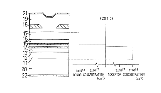
Fig. 1(a) is a cross sectional view showing a first
embodiment of the present invention. In this semiconductor
laser device, on a semiconductor substrate (n-GaAs) 20 formed
in sequence are a second n-type clad layer (n-Alo.asGao.szAs with
a donor concentration of 1x1018cm-3 and a thickness of 0.7 um)
11, a first n-type clad layer (n-A1o,31Gao.6sAs with a donor
concentration of 1x1018cm-3 and a thickness of 0.4 um) 12, an
n-type carrier blocking layer (n-Alo.soGao.aoAs with a donor
concentration of 1x1018cm-3 and a thickness of 0.014 um) 13, an
active layer (DQW: double-quantum well of GaAs/Alo.siGao.s9As
without doping) 14, a p-type carrier blocking layer (p-
Alo.soGao.soAs with an acceptor concentration of 1x1018cm-3 and
a thickness of 0.021 pm) 15, a first p-type clad layer (p-
Alo.siGao.69As with an acceptor concentration of 1x1018cm-3 and
a thickness of 0.4 pm) 16, a second p-type clad layer (p-
A1o,48Gao.szAs with an acceptor concentration of 1x1018cm-3 and
a thickness of 0.7 pm) 17, an current constriction layer (n-GaAs
with a donor concentration of 1x1018cm-3 and a thickness of 0.3
dun) 18, and a p-type contact layer (p-GaAs with an acceptor
concentration of 3x101'cm-3 to 1x1019cm-3 and a thickness of 2
- 18 -
CA 02208999 1997-06-27
~.un) 19 by metal organic chemical vapor deposition (MOCVD),
where Se ( selenium) is doped as donor and C ( carbon ) is doped
except the p-type contact layer where Zn is doped.
Ohmic electrodes 21 and 22 are provided on the top of the
p-type contact layer 19 and the bottom of the semiconductor
substrate 20 respectively.
Fig. 1(b) is a profile diagram showing the doping
concentration of the layers from the second n-type clad layer
11 to the second p-type clad layer 17.
It should be noted that the p-type carrier blocking layer
15 is doped with carbon.
Comparison 1 employs zinc used as the acceptor and its
other structure is identical to that of Embodiment 1.
Figs. 5 and 6 are profile diagrams showing the
concentration of various elements near active layer in a
semiconductor laser device having a perfect-SCH formed by MOCVD .
Fig. 5 corresponds to Embodiment 1 where carbon (C) is used
as the p-type dopant . Fig. 6 corresponds to Comparison 1 where
zinc ( Zn ) is used as the p-type dopant . The n-type dopant is
selenium ( Se ) in both the cases . Samples used in Figs . 5 and
6 are intended for measurement of the concentration. The
sample of Fig. 5 is distinguished from the sample of Embodiment
1 by the fact that the p-type carrier blocking layer is made
of Alo,6oGao.aoAs and the first clad layer is made of Alo.aoGao.7oAs.
Also, the sample of Fig. 6 is distinguished from the sample
- 19 -
CA 02208999 1997-06-27
of Comparison 1 by the fact that the p-type carrier blocking
layer is made of Alo,so~ao.aoAs.
Each of the profiles shows a measurement of signal
intensity with the element concentration detected by secondary
ion mass spectrometer (SIMS) along the ordinates and a depth
in the layer along the abscissa. The depth D1 corresponds to
the position of the p-type carrier blocking layer and the depth
D2 corresponds to the position of the n-type carrier blocking
layer.
Refering to the A1 content x shown in Fig. 5, it is intended
that x=0.3 in the first p-type clad layer which is shallower
than D1, x=0.6 at D1 in the p-type carrier blocking layer, x<0.3
in the active layer between D1 and D2 , x=0 . 6 at D2 in the n-type
carrier blocking layer, and x=0. 3 in the first n-type clad layer
which is deeper than D2. The Al content relates to the width
of the band gap, namely the band gap is minimum in the active
layer and maximum in both the carrier blocking layers. The
active layer has a double-quantum well structure and its
profile should exhibit more rises and falls, which are
moderated due to the resolution of SIMS.
The element concentration of carbon do in Fig. 5 is
1x1018cm-3 in a region shallower than D1 and almost nil in a region
deeper than D2. ,
Also, the element concentration of selenium ds in Fig.
is almost nil in a region shallower than D2 and 1x1018cm-3 in
- 20 -
CA 02208999 1997-06-27
a region deeper than D1.
In Fig . 6 , the A1 content x and the selenium concentration
ds show profiles similar to those in Fig. 5, both are
substantially consistent to each other respectively.
The element concentration of zinc dz in Fig. 6 is 1x1018cm-3
in a region shallower than D1 and gradually declined towards
D1. It is almost a half the peak value at D1. As apparent,
the diffusivity of zinc is high. When the carrier blocking
layer is thin, zinc will easily escape to the other layers hence
hardly producing a high doping concentration. It is also
apparent that the active layer is polluted with zinc.
On the other hand, carbon is an element low in the
diffusivity and its doping concentration can be high even when
the carrier blocking layer 15 is very thin. This prevents
adverse depletion throughout the layer. Magnesium shows such
a similar profile as that of carbon.
For comparison between Embodiment 1 and Comparison 1, the
result of measuring the characteristic temperature and the
internal loss of the semiconductor laser devices are shown in
the following table ( Table 1 ) . The layer construction, the Al
content x, and the doping concentration are identical to each
other. A difference of Comparison 1 from Embodiment 1 is that
the p-type carrier blocking layer 15 is doped with zinc . The
other conditions including 700 um of cavity length, 50 um of
current injection stripe width, and no optical coatings in the
- 21 -
CA 02208999 1997-06-27
semiconductor laser devices are also identical. It is found
from the comparison that the characteristic temperature
representing the temperature dependence of oscillation
threshold is improved from 120 K to 140 K. This may be explained
by the fact that as the doping concentration in the carrier
blocking layers is maintained to a desired level with the use
of a dopant of carbon which is lower in the diffusivity than
s
zinc, the carriers are successively confined in the active
layer as compared with the case of zinc.
- 22 -
CA 02208999 1997-06-27
Table 1
Embodiment Embodiment Comparison Comparison
1 2 1 2
Dopant Carbon Carbon Zinc Zinc
Doping
Concentration
( cm_3 )
Carrier 1x10¹⁸ 1x10¹⁸ 1x10¹⁸ 1x10¹⁸
blocking layer
First clad 1x10¹⁸ 3x101' 1x10¹⁸ 3x101'
layer
Second clad 1x10¹⁸ 3x101' 1x10¹⁸ 3x101'
layer
Characteristic 140 140 120 90
Temp. (K)
Internal loss 10 2 10 2
( cm' 1 )
Embodiment 2
Fig. 7(a) is a cross sectional view showing a second
embodiment of the present invention. In this semiconductor
laser device, on a semiconductor substrate (n-GaAs) 20 formed
in sequence are a second n-type clad layer (n-A1o,48Gao.saAs with
a donor concentration of 3x101'cm-Sand a thickness of 0.7 um)
11, a first n-type clad layer (n-Alo.siGao.s9As with a donor
concentration of 3x101'cm-3 and a thickness of 0.4 um) 12, an
n-type carrier blocking layer (n-Alo,soGao.aoAs with a donor
concentration of 1x1018cm-3 and a thickness of 0.014 pm) 13, an
active layer (DQW: double-quantum well of GaAs/Alo.siGao.s9As
- 23 -
CA 02208999 1997-06-27
without doping) 14, a p-type carrier blocking layer (p-
Alo.soGao.soAs with an acceptor concentration of 1x1018cm-3 and
a thickness of 0.021 um) 15, a first p-type clad layer (p-
A1o.31Gao.ssAs with an acceptor concentration of 3x101'cm-3 and
a thickness of 0.4 um) 16, a second p-type clad layer (p-
A1o,48Gao,s2As with an acceptor concentration of 3x101'cm-3 and
a thickness of 0.7 um) 17, an current constriction layer (n-GaAs
with a donor concentration of 1x1018cm-3 and a thickness of 0.3
um) 18, and a p-type contact layer (p-GaAs with an acceptor
concentration of 3x101'cm-3 to 1x1019cm-3 and a thickness of 2
um) 19 by metal organic chemical vapor deposition (MOCVD),
where Se is doped as donor and C is doped as acceptor except
the p-type contact layer where Zn is doped.
Ohmic electrodes 21 and 22 are provided on the top of the
p-type contact layer 19 and the bottom of the semiconductor
substrate 20 respectively.
Fig. 7(b) is a profile diagram showing the doping
concentration of the layers from the second n-type clad layer
11 to the second p-type clad layer 17. It should be noted that
both the donor concentration in the n-type carrier blocking
layer 13 and the acceptor concentration in the p-type carrier
blocking layer 15 are set to 1x1018cm-3 or higher while the donor
concentration in the second 11 and the first n-type clad layer
12 and the acceptor concentration in the first 16 and the second
p-type clad layer 17 are set to 3x101'cm-3 or lower as shown in
- 24 -
CA 02208999 1997-06-27
Fig. 7(b), i.e. the modulation doping is applied.
Since the carrier blocking layers 13 and 15 are maintained
high in the doping concentration, the depletion of the layers
13 and 15 is suppressed as a whole thus producing a higher
potential barrier and efficiently confining injected carriers
in the active layer 14. As the doping concentration in a light
leaking region or the clad layers 11, 12 , 16 , and 17 is formed
to a low level, the absorption of free carriers will be decreased
thus improving the laser oscillation efficiency. The
result of measuring the characteristic temperature and the
internal loss in the semiconductor laser device of Embodiment
2 are also shown in Table 1 under the conditions including 700
um of cavity length, 50 um of current injection stripe width,
and no optical coatings. As compared with Embodiment 1, the
internal loss is remarkably reduced to 1/5 while the
characteristic temperature remains unchanged.
Comparison 2 is substantially identical to Embodiment 2 ,
except that zinc is doped as acceptor.
Fig. 8 is a graphic diagram showing the concentration of
various elements near the active layer in a sample
corresponding to Embodiment 2 in which the p-type dopant is
carbon (C). Fig. 9 is a similar diagram corresponding to
Comparison 2 in which the p-type dopant is zinc (Zn) . In both
the cases, the n-type dopant is selenium (Se). Samples used
in Figs. 8 and 9 are intended for measurement of the
- 25 -
CA 02208999 1997-06-27
concentration. The sample of Fig. 8 is distinguished from the
sample of Embodiment 2 by the fact that the p-type carrier
blocking layer is made of Alo,soGao.aoAs and the first clad layer
is made of Alo,soGao.7oAs. Also, the sample of Fig. 9 is
distinguished from the sample of Comparison 2 by the fact that
the p-type carrier blocking layer is made of Alo.6oGao.aoAs .
The profiles like those shown in Figs. 5 and 6 show
measurements of signal intensity with the element
concentration detected by SIMS along the ordinates and a depth
in the layer along the abscissa. The depth D1 corresponds to
the position of the p-type carrier blocking layer and the depth
D2 corresponds to the position of the n-type carrier blocking
layer.
Referring to the Al content x shown in Fig . 8 , it is
intended that x=0.3 in the first p-type clad layer which is
shallower than D1, x=0 . 6 at D1 in the p-type carrier blocking
layer, x<0.3 in the active layer between D1 and D2, x=0.6 at
D2 in the n-type carrier blocking layer, and x=0. 3 in the first
n-type clad layer which is deeper than D2.
The element concentration of carbon do in Fig. 8 is
3x101'cm-3 in a region shallower than D1, 1x1018cm-3 at D2 , and
almost nil in a region deeper than D2.
Also, the element concentration of selenium ds in Fig.
8 is almost nil in a region shallower than D2 , 1x1018cm-3 at D2 ,
and 3x101'cm-3 in a region deeper than D2.
- 26 -
CA 02208999 1997-06-27
In Fig . 9 , the A1 content x and the selenium concentration
ds show profiles similar to those in Fig. 8, both are
substantially consistent to each other.
The element concentration of zinc dz in Fig . 9 is 3x101~cm-3
in a region shallower than D1 and gradually declined towards
D1. At D1, no peak is shown. As apparent, the diffusivity of
zinc is high and when the carrier blocking layer is thin, zinc
will easily escape to the other layers hence hardly producing
a high doping concentration.
On the other hand, carbon is an element low in the
diffusivity and its doping concentration can ideally be high
even when the carrier blocking layer 15 is very thin . Magnesium
shows such a similar profile as that of carbon.
The result of measuring the characteristic temperature
and the internal loss of the semiconductor laser device of both
Embodiment 2 and Comparison 2 are also shown in above Table
1 under the conditions including 700 um of cavity length, 50
um of current injection stripe width, and no optical coatings .
The sample of Comparison 2 is distinguished from that of
Embodiment 2 by the fact that zinc is doped as acceptor. As
compared with Comparison 2, the characteristic temperature is
remarkably improved from 90K to 140K.
The normalized frequency V of Embodiments 1 and 2 is ~c.
The present invention may be implemented with the normalized
frequency of n/3 or smaller. It is however preferred that the
- 27 -
CA 02208999 1997-06-27
normalized frequency V is more than n/3 because the optical
damage on the output end facets is suppressed to allow a higher
output with ease.
Although both the first and second clad layers have a low
concentration in Embodiment 2 , the first clad layer which is
nearer to the active layer only may have a low concentration .
Embodiment 3
Fig. 10(a) is a cross sectional view showing a third
embodiment of the present invention . Fig . 10 ( b ) is an enlarged
cross sectional view of an active layer 14.
In this semiconductor laser device on a semiconductor
substrate ( n-GaAs ) 20 formed in sequence are a second n-type
clad layer (n-Alo,aaGao.szAs with a donor concentration of
1x1018cm-3 and a thickness of 0.7 pm) 11, a first n-type clad
layer (n-Alo.3oGao.~oAs with a donor concentration of 3x101'cm-3
and a thickness of 0 . 4 pm) 12 , an n-type carrier blocking layer
(n-Alo,6oGao.aoAs with a donor concentration of 1x1018cm-3 and a
thicknes s of 0 . 014 um ) 13 , an active layer ( SWQ : single-quantum
well) 14, a p-type carrier blocking layer (p-Alo,soGao.soAs with
an acceptor concentration of 1x1018cm-3 and a thickness of 0. 021
um) 15, a first p-type clad layer (p-Alo,3oGao.~oAs with an
acceptor concentration of 3x101'cm-3 and a thickness of 0.4 um)
16, a second p-type clad layer (p-A1o,48Gao.saAs with an acceptor
concentration of 1x1018cm-3 and a thickness of 0.7 um) 17, a
current constriction layer (n-GaAs with a donor concentration
- 28 -
CA 02208999 1997-06-27
of 1x1018cm-3 and a thickness of 0.3 ucn) 18, and a p-type contact
layer (p-GaAs with an acceptor concentration of 3x101'cm-3 to
3x1019cm-3 and a thickness of 2 um) 19 by MOCVD, where Se is doped
as donor and C is doped as acceptor except the p-type contact
layer where Zn is doped.
Ohmic electrodes 21 and 22 are provided on the top of the
p-type contact layer 19 and the bottom of the semiconductor
substrate 20 respectively. Incidentally a laser beam is
propagated along a direction vertical to the sheet of paper
and oscillated between the two end facets constituting an
optical resonator.
As shown in Fig. 10(b), the active layer 14 has a
single-quantum well structure, where formed in upward sequence
are an undoped barrier layer (Alo.soGao.7oAs with a thickness of
0.038 um) 34, a p-type doped barrier layer (p-Alo.aoGao.7oAs with
a carbon doped acceptor concentration of 1x1018cm-3 and a
thickness of 0.010 pm) 35, an undoped barrier layer
(Alo,3oGao,~oAs with a thickness of 0.002 um) 36, a quantum well
layer (GaAs with no doping and a thickness of 0.004 um) 37,
an undoped barrier layer (Alo.3oGao.~oAs with a thickness of 0.002
pm) 38, a p-type doped barrier layer (p-Alo.soGao.~oAs with a
carbon doped acceptor concentration of 1x1018cm-3 and a
thickness of 0.010 um) 39, and an undoped barrier layer
(Alo.soGao.7oAs with a thickness of 0.038 um) 40.
It should be noted that particular ones of the barrier
- 29 -
CA 02208999 1997-06-27
layers in the single-quantum well structure of the active layer
14 are doped with carbon. The holes formed by the carbon doping
are localized in the quantum well layers to contribute to the
increase of optical gain. As the result, the quasi-Fermi level
descends and the potential barrier in each carrier blocking
layer ascends relatively. As the efficiency of carrier
confinement is increased, the characteristic temperature of
the semiconductor laser device will be improved. Also, the
quantum well layers can be maintained undoped, avoiding
broadening of the light emission spectrum.
For comparison, a semiconductor laser device was prepared
in which the p-type doped barrier layers 35 and 39 are replaced
by undoped barrier layers. It was found through measurement
under the common conditions including 1500 um of cavity length,
50 p.m of current injection stripe width, and no optical coating
that the characteristic temperature representing the
temperature dependence of oscillation threshold is 110K in the
comparison and 140K in Embodiment which is about 30 ~ higher.
In this Embodiment described above the p-type doped
barrier layers 35 and 39 are doped with carbon , they may be
doped with magnesium or the like which is low in the diffusivity.
The active layer 14 is not limited to the single-quantum
well structure but may consist of a multi-quantum well
structure (MQW) having two or more quantum wells.
In these embodiments described above the semiconductor
- 30 -
CA 02208999 1997-06-27
laser devices employ an AlGaAs base semiconductor compound,
they may employ any other appropriate material in which carbon
or magnesium can be used as p-type dopant.
ADVANTAGEOUS EFFECT OF INVENTION
As set forth above, the present invention allows the
p-type carrier blocking layers to be doped with carbon or
magnesium and, even when the carrier blocking layers are thin,
have an adequate doping concentration, hence ensuring the
carrier confinement into the active layer by the carrier
blocking layer. This will largely contribute to the
improvement of the characteristic temperature. Also, the
quantum well layers can remain undoped hence avoiding
broadening of the light emission spectrum.
In addition, the concentration of free carriers in the
clad layers in which light is propagated can be reduced, whereby
the internal loss can be decreased. The optical damage on the
output end facets can be suppressed thus permitting a higher
output.
The present invention also allows the barrier layer in
the quantum well structure of the active layer to be doped with
carbon or magnesium to increase the concentration of holes in
each quantum well. This lowers the quasi-Fermi level of
electrons in the active layer hence decreasing the probability
of electrons overflow from the active layer. Accordingly, the
efficiency of carrier confinement in the active layer can be
- 31 -
CA 02208999 1997-06-27
improved thus improving the laser oscillation efficiency and
the characteristic temperature.
As the result, a high-efficiency, high-output
semiconductor laser device with perfect SCH can be obtained.
- 32 -