Note: Descriptions are shown in the official language in which they were submitted.
CA 02209019 1997-06-27
W O 96t21254 PCTlCAg6/00012
AN ANTE-NNA FOR A PORTA~LE RADIO COMMUNICATION DEVICE
FIELD OF THE INV~ENTION
The present invention concerns radiation reduction a~aldlus of a type int~nt1.ocl to be used in
conjunction with ha 1d-held or otherwise portable radio phones and the like to reduce, re-direct, or
redistribute away fi om a user or other radiation ~ ip~tive medium radiation emitted from the
radiation emitting s~ructure of the phone, such as the ~ntt~ n~
BACKGROUND CiF THE INVENTION
Cellular and other portable radio telephones typically have ~ntPnn~ which extend from the housing
ofthe phone. While the phone is in use the ~ntPnn~ emits radiation which has caused concern among
the medical cornm- nity as to the radiation's effects on the user of the phone.
The use of flexible protective shields to protect personnel against X-ray frequency and Gamma
frequency radiation such as may be emitted by X-ray m~rhinPs or by nuclear reactors, respectively,
is known in the art as illustrated by U.S. Patent No. 3,039,001 entitled "Flexible Protective Plastic
Shield" and by United States Patent No. 5.012.114 entitled "Radiation Shield".
UnitedStatesPaten~No.3,039,001 disclosesthatasheetofvinylorotherplasticmaterialc~"l~i,.;..g
resin, plasticizer and stabilizer may have a protective material such as pulverized lead uniformly
~5 distributed thereth.ough in order to provide a flexible sheet of m~teri~l which protects the wearer
against X-rays. (T~nm~ rays. Neutron rays, secondary cosmic rays and the like.
o
United States Pater t No. 5~01~.1 14 discloses a gamma radiation shield which comprises a wrappable
sheet of garnma radiation .chiel~lin~T m~trri~l to which is affixed releasable contact-f~t~ners, which
30 are so ~lim~.n~ioned and configured that when a shield member is wrapped around a gamma radiation
CA 02209019 1997-06-27
W O96/21254 PCT/CAg6/00012
emitting structure, compliment~ry locking portions of the releasable f~t~ners engage each other to
securely hold the shield member in shielding position wrapped around the structure. The gamma
radiation shielding m~t~ri~l may be compri~e~l ofthe known construction of fine lead powder being
uniformly dispersed in a matrix of thermo-plastic m~t.-ri~l which serves as a binder for the lead
5 powder so as to form a flexible sheet. The releasable contact-f~teners may be of a type sold under
the trade-mark Velcro. The patent is directed to protecting personnel in nuclear reactors and the like
by shielding conduits such as pipes, most clearly seen in Figure 6 of the patent, through which
radioactive material flows.
1~ The use of electrom~gnetic shielding to minimi7~ hltelr~l~nce between electromagnetic signals
- radiated by cellular phones and like electronic eqllipm~nt with another portion of that equipment and
the minimi7~tion of such illLelr~lcllce by interposing electrically conducting material in the form of
a shield between the source of the electromagnetic signals and the ~ ;Uilly subject to interference
is taught by United States Patent No. 5,124,889 entitled "Electromagnetic Shielding Apparatus for
Cellular Phones". The reference to electrom~gnetic shielding does not appear to be concerned with
protecting the user of the electronic device from radiation from the ~ntenn~ or the like.
With portable radio telephones such as hand-held cellular phones, radio waves that carry the call
em~n~te directly from the telephone, specifically the length of the telephone and antenna, most
intensely at a midpoint there along, while the telephone is held to the ear of the user. There is
concern that the radio frequency waves entering the dissipative medium of the user's head may cause
heating. cancer or DNA fragmentation.
There is ~;ull~llll~y being marketed a cellular phone radiation shield being sold under the trade-mark
"Cellguard", m~nllf~t7lred by QU~1LU111 Laboratories of Renton, Washington, U.S.A. As discussed
in more detail below, the "Cellguard" device consists of two sections of molded plastic, each with
metal inside, that serves to block or deflect the radio frequency signal. One part of the device covers
the phone's antPnn~ and the other part fits over the earpiece of the phone. The metal of the Cellguard
- device is placed between the ~ntPnn~ and the user and between the earpiece and the user. A similar
device, that is, an arrangement in which a radiation shielding device is placed between the ~ntenn~
CA 02209019 1997-06-27
w o96r2l2s4 . PCTICAg6/00012
and the user is taught in U.S. Patent No. 5,335,366 which issued to Daniels on August 2, 1994. In
particular, Daniels liscloses a radiation shielding a~p~lus for a radio tr~n~mitting device having
a radiation shield disposed between the zlnt~nn~ and a user, the radiation shield for absorbing,
blocking and/or ref~ecting electromagnetic wave radiation.
s
United States Paten- No. 5,336,896 which issued to Katz on August 9, 1994 for a cellular telephone
users protective device teaches a cellular telephone accessory both for protecting a user from
electromagnetic radiation and for providing a handle for the cellular phone. In particular, a tilt and
swivel base is taugh.t to permit moving the cellular phone ~nt~nn~ away from close contact with the
10 user's head and to also supply a calTying handle. What is further taught is providing a protective
magnetic radiation shielded jacket to contain the cellular phone within the jacket, the ~ntenn~ tilt and
swivel base attached to the outside of the jacket.
The present invention has at least five objects. The first object, in one embodiment, is to reduce the
15 overall amownt of e .ectr~ m~gn~.tic radiation emitted by redl~c.ing the emitted power of the ~nt~nn~
The second object. in a further embodiment, is to redistribute the radiation in the vicinit,v of the
phone and in particlllar the ~nt~nn~, ie. in the near field, away from an associated ~ ip~tive mt~ lm
such as the head of a user. Consistent with this object, the present invention changes the near field
radiation pattern sw-Townding a radio cullllllul~icatiOn device such as a radio phone, and in particular
20 surrounding the de~ice's ~ntenn~ so that: (a) a reduction is ~tt~in~cl in radiation field strength dw~ing
tr~n~mi~sion there~y re~lucing "hot spots" at the associated ~ ir~tive mediwm such as the user's
head; (b) a reduction is attained in the amount of radiated energy during tr~n.~mi~sion which is
absorbed by the ass3ciated (~ ir~tive mediwm, to thereby increase the effective power of the radio
tr~n~mi.~sion, and, (c) an increase is attained in the effectiveness of the ~ntenn~ during reception of
25 radio tr~n.~mi~sions by an increase in the effective exposwre of the ~nte.nn~
The third object is to accomplish the above objects without significantly adversely affecting the
operation of a radio coll~ ication device such as a cellular telephone within a cellular telephone
communication sys.:em, which adverse operation may result if the ~nt~nn~ excessively loses r~ ting
30 power or becomes excessively directional. In the case of cellular telephones it is desirable that the
CA 02209019 1997-06-27
W O 96/21254 PCT/CA96/00012
far field radiation pattern does not have large signal strength variations with the direction in which
the signal is sent. It is desired that the user can hold the cellular telephone in a random orientation
without concern about the direction in which the signal must travel in order to reach the center of
the cell. Modification of an ~ntenn~ can result in large changes to the far field radiation pattern.
5 Since this is undesirable, it is an object of the present invention to not cause large changes to the far
field radiation pattern while at the same time, over the entire desired operational bandwidth,
- minimi~ing the near field "hot spots" on an associated tli~ip~tive medium where radiation strength
is excessive, mininni7ing the amount of radiation absorbed by the dissipative medium, and
m~ximi~ing the effective exposure of the ~ntPnn~ to reception of radio tr~n~mi~sions.
The fourth object is to avoid damage or undue strain on the internal electrical ch-;uill~y of the cellular
phone. Such damage is conceivable in a situation where a modification to the ~ntenn~ results in a
greater electrical load being placed on the electrical ~;ill.;UiLI~/ SO that a greater current flows through
parts of the cellular phone. If this increased current exceeds the limits contemplated by the de~igners
15 of the cellular phone, some internal parts of the cellular phone could have their operation impaired
or could malfunction.
The fifth object is to m~int~in operation of the receiving function of the cellular telephone to an
acceptable degree. The ~ntPnn~ of the cellular telephone ~imnlt~neously operates with two
20 functions. One is to transmit signals, and it is this function that results in high intensity radiation
being present in the vicinity of the cellular telephone. The second function of the ~ntPnnZl is to
receive signals from a distant source, convert these signals into oscillating electrical currents which
are converted by the circuitry of the cellular telephone into a voice message heard by the user. It is
conceivable that modifications to the ~nt~.nn~ could decrease the ability of the cellular phone to
25 clearly receive these incoming signals. It is an object of the present invention to not cause
unacceptable reduction in the quality of these incoming signals, but in fact to increase the reception
quality by increasing the effective exposure of the ~ntennz~
CA 02209019 1997-06-27
W O96121254 .- PCT/CAg6JOOnl2
SUMMARY OF l'HE INVENTION
The present invent.on is, in a first embodiment, a radiation redllcin~ or re-directing device suitable
for use on or in conjunction with cellular phone c~ntenn~, or radiation emitting structures of portable
5 radio communica~ion devices. The device has ~ntP.nn~ near field radiation pattern redistribution
means for redistril~uting near field radiation away from a user of the radio commlmic~tion device,
the antenna near field radiation pattern redistribution means mountable in proximity to a radio
communication dcvice and in particular the ~ntçnn~, and in a further embodiment, on an opposed
side of the antenna or of the radio col.,.ll~ication device (for example, where the device does not
10 have an ~ P~ o the user. The device may also include an ~ntPnn~ power reduction means for
reducing the antenna power. The m~fçri~l~ out of which the device is made may include dielectric
materials, magnetically permeable m~tçri~l~7 conductive m~t~ri~l~, in~ tinp; m~tP.ri~
semicon~ tin~ materials, superconducting msltçri~lc, or any combination of these materials.
Dielectric m~trri~ are understood to include m~t.o.ri~l~ whose permittivity exceeds the permittivity
15 of free space, or which act to diffract electromagnetic waves of a wavelength relevant to the
operation of a rad o comrnunication device, or which slow down the propagation of electrom~gn~tic
waves of a wavelength relevant to the operation of a radio coll~nu"ication device. In particular, the
dielectric materia! may have, in order of prer~lellce, a dielectric constant of at least 3, of at least 6,
of at least 9, of at least 12, and of at least 15
The structure of t.he device may be of an cul.ill~.y shape of a m~tPri~l, in any number of pieces. The
structure may be layered, or mixed in any manner, including the application of thin layers in the
interior or on the surface. The structure can include electronic components which have the effect
of decreasing the electrical current in the ~ntPnn~ or otherwise reducing the power of the radiation
25 emitted by the antenna. That is, the present invention may consist of any electrical device which is
placed between the cellular phone ~ntPnn~ connection point and the c~ntPnn~ whose effect is to
provide an electr cal impedance to the antenna current. This includes, but is not limited to, devices
having resistance, ç~p~cit~nce, or intlll~t~nre7 or a combination of these properties. The device may
also attach to the free end of the ~ntçnn~
-
CA 02209019 1997-06-27
W O 96/212S4 PCT/CAg6/00012
The structure of the device may be placed in the proximity of an ~ntenn~, or in contact with the
~nt~nn~ or may form an extension of the ~nt~nn~ or may form a component of the z~ntenn~ or may
replace the existing ~ntenn~ of a radio co~ unication device. The device does not, however, act
as a shield so as to come between an e~i~ting radiation emitting structure such as an ~ntenn~ and
5 parts of the user's body which are closest to the radiation emitting structure.
The present invention may also consist of a device between the cellular phone and the ~nt~nn~ built
in to the cellular phone, which provides the user with the ability to adjust the effect of the device so
that the intensity of the radio waves may be adjustably made greater or smaller. This could be a
10 variable capacitor, variable resistor or variable inductor, but it is not restricted to these.
The present invention could take any of the forms mentioned above and also have provision for
adjustment by the user to attain greater or lesser intensity of radio waves.
,
15 The present invention could take any of the forms mentioned above and also have automatic
provision for adjustment, ie. reduction, of the intensity of emitted radio waves. This automatic
adjustment could be triggered by sound level and accomplished by built-in ci~;uilly, or a device
-~ could be electrically attached to the cellular phone to accomplish the automatic adjustment.
20 In a further embodiment, the present invention may take the form of an improved antenna fbr a
portable radio comm~mication device which includes, a first elongate electrically conductive member
having opposed first and second ends, where the first end is adapted to be mounted in electrical
communication to a radio communication device, whereby when the first elongate electrically
conductive member is mounted in electrical communication to a radio communication device, a
2~ radiation field pattern is generated by radiation emitted by the first elongate electrically conductive
member and the radio communication device during radio tr~n.~mi.~.cion, the radiation field pattern
having maximum intensity at a first location, the device also including means for increasing
radiation resistance of the first elong;~te electrically conductive member mountable at an optimized
position at generally the second end, whereby, when the means for increasing radiation resistance
-: 30 is mounted to the first elongate electrically conductive member at the ~limi~d position at generally
~ . ,
CA 022090l9 l997-06-27
W O 96/212S4 PCT/CAg6JO0012
the second end and the first elongate electrically conductive member is mounted in electrical
communication to a radio communication device, during radio trS1nsmi.ssion the radiation field
pattern maximum illtensity is shifted from the first location to a second location closer to the second
- end, and near field :.ntensity of the radialion field pattern at the first location, i.e. by the users head
5 for example, is rec uced over an operational bandwidth of the radio communication device.
In an alternative further embodiment, the present invention may take the form of an ~ntçnn~
improvement device for a portable radio collllllu.lication device ~ntenn~, wherein the anterma is a
first elongate electr~cally conductive member having opposed first and second ends and the first end
10 is adapted to be mounted in electrical coll~ll~ication to a radio collllllulfication device, and wherein
when the first elon Jate electrically conductive member is mounted in electrical communication to
a radio comrnunica,ion device a radiatio:n field pattern is generated by radiation emitted by the first
elongate electrica].ly conductive member and the radio communication device during radio
tr~nsmi~.si-n,ther~diationfieldpatternhavingmz.xi"""~ intensityatafirstlocation,forexample,
15 by the users head or other undesirable ~lissip~tive medium. The ~ntçnn~ improvement device
including: means t~or increasing radiation resist~nce of the first elongate electrically conductive
member mountable at an optimized position at generally the second end, whereby, when the means
for increasing radii.ltion resistance is mounted to the first elongate electrically conductive member
at the optimized position at generally the second end and the first elongate electrically conductive
20 member is mounted in electrical collllllullication to a radio communication device, during radio
tr~nsmis.sion the r~diation field pattern m~xi,,,~,,, intensity is shifted from the first location to a
second location clc.ser to the second end, and near field illt~llsi~y of the radiation field pattern at the
first location is rec uced over an operational bandwidth of the radio communication device.
2~ Advantageously~ i~ both the ffirther ernbodiment and the ~ltern~tive embodiment, the means for
increasing radiation resistance of the fir~t elongate electrically conductive member is a short parasitic
element, which may be a helical electrically conductive coil, wherein the helical electrically
conductive coil m,ay be mountable ove:r the second end to thereby journal the second end within a
cavity within the helical electrically conductive coil at least partially along the cavity so as to
CA 02209019 1997-06-27
W O96/21254 PCTICAg6/00012
optimize ~nt~nn~ p~lrollll~lce by re~ ing near field radiation intensity at the first location without
substantially adversely affecting far field performance.
Alternatively, the short parasitic element may be a short second elongate electrically conductive
5 member mountable generally adjacent and parallel to the first elongate electrically conductive
member.
In the present invention, the ~ntenn~ may be a monopole ~ntenn~
10 In the further embodiment and alternative further embodiment of the present invention, the radio
communication device radiation has a range of operational wavelengths corresponding to the
operational bandwidth and the short parasitic element may have a length of less than approximately
- three-quarters of one-half of a wavelength within the range of operational wavelengths. The short
- parasitic element may advantageously have a length of ~ Jx i ~ tely 1/20th of a wavelength within
15 the range of operational wavelengths.
- In the present invention, the short parasitic element may be a short length of dielectric material
mountable generally adjacent and parallel to the first electrically conductive member.
- ~0 The dielectric material is an inert matrix impregnated with heavy metal, where the heavy metal may
be heavy metal powder, and where the inert matrix may be flexible. The inert matrix impregnated
with heavy metal may be lead vinyl. In the further embodiment and the alternative further
embodiment of the present invention, the means for increasing radiation resistance may include
means for increasing capacitance of the first elongate electrically conductive member. The means
25 for increasing capacitance of the first elongate electrically conductive member may be conductive
material, where the conductive material may be mountable into the second end.
The means for increasing radiation resi~t~n~e may include means for decreasing current in the first
elongate electrically conductive member, where the means for decreasing current is an inductor,
CA 02209019 1997-06-27
W O 96/21254 P ~/CA96~WO~
resistor, or cz-rRcit~r. The means for decreasing current may be mountable between the first elongate
electrically conductive member and the radio co~ ~ication device at the first end.
The means for increasing capacitance of the first elongate electrically conductive member may
5 ~lt~ tively be a length extension of the first elongate electrically conductive member mountable
onto the first elongate electrically conductive member whereby the first elongate electrically
conductive member may be mi~m~tr.hed to cil~;uill~ within the radio col,,,,,ll,,iç~tion device. The
length extension may be mountable onto the second end. Further, ~lt~ tively, the means for
increasing capacit;mce of the first elon~ate electrically conductive member may be a replacement
10 first elongate eleckically conductive member, where the replacement first elongate electrically
conductive member is longer than the first elongate electrically conductive member and the
replacement first e Longate electrically conductive member may be substituted for the first elongate
electrically conductive member.
15 The present invention, may further include means for adjusting the c~p~cit~n(~e of the means for
increasing capacitance.
In the ~ltern~tive embodiment and further alternative embodiment, the short parasitic element may
be tilted so that its longitudinal axis of the ~ntenn~ whereby, because of the directional
20 characteristics of the short parasitic element, tilting the longit~lllin~l axis of the short parasitic
element towards the ~ ir~tive medium at the first location may accomplish a further reduction in
near field radiatio~ intensity at the first location.
B~IEF DESCRI~TION OF THE DRAWINGS
In the drawings, ~rhich represent specific embodiments of the present invention, but which should
not be construed as limitin~ the scope of the invention in any way:
CA 02209019 1997-06-27
W O 96/21254 . PCT/CAg6/00012
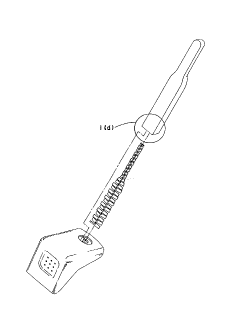
Figures 1 (a), 1 (b) and 1 (c) are, respectively, an exploded perspective view of the Cellguard device,
a fr~gm~nt~ry partially cut away view of the base of the Cellguard ~nt~nn~ cover, and a reverse
perspective view of the Cellguard earpiece cover.
5 Figures 1 (c) and 1 (d) are schematic views of the operation of a prior art radio communication
device ~ntenn~
Figure 2 is a cross-sectional view along lines 2 - 2 in Figure 3 illustrating a time averaged near field
radiation pattern.
- Figure 3 is, in perspective view, a radio CO~ cation device inco~porating one embodiment of the
radiation reduction a~pa,~ s of the present invention.
Figure 4a is a diagram illustrating the radiation pattern associated with prior art hand held portable
15 communication devices.
Figure 4b is the diagram of Figure 4a illustrating a redistributed radiation field associated with the
= ~ improved ~nt~nn~ of the present invention.
- 20 Figure Sa is a front elevation view of a cellular telephone having an improved ~ntPnn~ of the present
- invention.
Figure 5b is the cellular telephone of Figure 5a with the ~ntenn~ casing partially cut away.
- ~5 Figure 5c is a side elevation view of a further embodiment of a cellular telephone having a
retractable improved ~ntenn~ according to the internal construction of Figure 5b.
Figures 6 (a) - 6 (e) and 6 (i) schem~tically illustrate alternative embodiments of the improved
antenna of the present invention for reducing ~nt~nn~ power. Figures 6 (f) - 6 (h) s-.hem~tically
30 illustrate adjustable antenna power reduction means.
.
CA 02209019 1997-06-27
W0 961212S4 . PCr~CA96~00012
Figure 7 is an enLIrged perspective view of an ~nt~nn~ insert embodiment incorporating one aspect
of the present invcntion.
- Figures 8 (a) - 8 (i) illustrate ~lt~ tive embo~limPnt~ of short parasitic elements incorporated in the
5 present invention.
Figure 9 is a front elevation view of a conventional ~nt~nn~ having a helical wire coil SPE mounted
thereon.
10 Figures 10 (a) - 1~) (e) illustrate ~ltt?rn~tive embo~liment~ of par~iti~lly top-loaded :mtt?nn~c
DETAILED DESCRIPTION OF PREFERRED EMBODIMENTS
The Cellguard Device:
As mentioned ab ~ve, the Cellguard device exists in the prior art. It is depicted in Figures 1 (a) -
1 (c). Testing of the flexible metal alloy strip of the Cellguard device indicates that it is likely a
carbon steel allo~ mostly comprised of chromium and iron. As may be seen, the geometric shape
of the metal alloy strip combined with the flexible p~ llies of the alloy, allow the alloy strip to be
20 flexed. although repeated flexing, it has been found, results in fatigue and eventual failure of the
alloy along the centre line of the alloy strip where the alloy is narrowest by design to accommodate
the flexing of the alloy strip. The base of the alloy strip electrically connects to a metal tab
ext~n-lin~ substar tially vertically from the earpiece covering portion of the Cellguard device. The
base of the alloy ~ trip and the metal tab are electrically connected, once in~t~llecl on a cellular phone,
25 to the casing of tk e cellular phone by metal-to-metal contact with the metal base of the ~ntenn~ (not
shown). The metll tab may be seen protruding vertically from the ea~piece cover in Figure 1 (a) and
- may also be seen protruding vertically upwards through the ~ntenn~ receiving hole in the earpiece
cover as depicte1 in Figure 1 (c). The metal alloy strip depicted in Figure 1 (a) is encased in a
urethane plastic moulding along the flat side of the moulding shown in Figure 1 (a) and better seen
30 in perspective partial cut-away view of Figure 1 (b).
CA 02209019 1997-06-27
W O96/21254 . PCT/CAg6/00012
The Cellguard device relies on a conventional method of shielding, namely, the electrical grounding
of conductive shielding material placed alongside a radiation source between the radiation source
and the object to be shielded.
5 Principles of Radio TrAnsmis.sion:
in tnis seclion, tne means by which the objects of the present invention are accomplished will be
explained with reference to an extremely simplified version of the operation of a cellular phone,
which is illustrated schem~tically in Figure 1 (d) and 1 (e). Figure l(d) illustrates the physical
10 arrangement of the cellular telephone. Note that only the circuitry that L.dllsll..L~ the signal from the
portable cellular telephone to the cell centre is shown. The entire cil~;uiLl y of the cellular telephone
is represented by a single device conventionally called a radio frequency (RF) oscillator. This RF
oscillator generates an alternating voltage at a frequency between 800 and 900 megahertz. One
termin~l of the RF oscillator is electrically connected to the chassis of the cellular telephone. The
15 other termin~l of the RF oscill~tc r is attached to a length of wire which forms the ant~nnA In fact,
during tran~mi.~.~ion not only the AntennA per se, but the Ant~nn~ and the conductive elements
- electrically connected to the RF oscillator act as an "Ant~nnA" so that the entire telephone, in this case
the AntennA and the chassis, radiate radiation. Because the radiation field is strongest at
approximately the mid-point of the overall ra~ ting body, the mAximum radiation intensity will be
20 at approximately where the cellular phone is held closest to the head of the user. The alternating
voltage from the RF oscillator forces Alt~.rn~ting current to flow in the Ant~?nnA This current creates
electric and magnetic fields in the air surrounding the AntennA These electric and magnetic fields
oscillate at the same frequency, between 800 and 900 megahertz. These oscillations ripple outwards
like waves on a pond surface, and carry the signal to the distant AntennA at the centre of the cell,
25 except where they are absorbed by the ~ ipAtive medium associated with the operation of a cellular
phone~ narnely, the ear, skull, brain etc. of the user.
~ The type of dissipative medium associated with a radio communication device will depend on the
particular application ofthe device. One example is the cellular telephone where health hazards have
30 been identified with the intense near field radiation strongest near the base of the Antt?nnA, which is
;
12
.
'''
CA 02209019 1997-06-27
W O96121254 . P ~CAg6~00012
emitted by the cel]ular phone and which causes hot spots in the user's head (where a "hot spot" is
a reference to the heating of the dissipative medium where the r~ tion from the ~nt~nn51 iS being
absorbed). Another example of a ~ tive mediurn associated with a radio col""~l"~ication device
- may be that of an antenna mounted in proximitv to a ~li.c~ipative medium such as radiation absorbing
5 m~teri~l used for cJrrent radar defeating technology. In such an application, much of the effective
ra-liating power o ~ the antPnn~ may be lost due to absolption of the radiation by the dissipative
medium unless the radiation field can, by the present invention, be redistributed away from the
dissipative mediuin without subst~nti~lly adversely affecting the far field performance of the
~nt~nn~
Figure l(e) schen ~tiç~lly depicts the cellular telephone of figure l(d), modified to schem~tically
illustrate the electrical properties of the circuit. The Ant~nn~ has three kinds of electrical properties.
The first is induct~nce, which is the characteri~tic of m~ ing a current in a wire once the current
is flowing. The second is capacitance, which is the characteristic of building up a stored charge in
15 an electrical component when voltage is applied. The third is resistance, which is the ratio of the
voltage applied across a conducting m~tPri~l to the current flowing through the c~-n-lncting m~tt~ri~l
The ~ntenn~ togerher with the circuitry inside the cellular telephone, has inductance, and the value
of this inductance is represented by the symbol Lant, and is understood to be expressed as a number
20 of Henries. The a~tenna, together with cir.;uilly inside the cellular telephone, has capacitance, and
the value ofthis c.lpacitance is represented by the symbol Cant, and is understood to be expressed as
a number of ~ar~ds. The ~nt~nn~, considered as a piece of wire, has an electrical resistance,
expressed by the s ymbol Rant~ and is understood to be expressed as a number of Ohms. In addition
to this, the internal circuitry of the cellular telephone has some resistance, which is expressed by the
25 symbol Rte,. Furthermore, the ~nt~nn~ has an extra resistance due to the creation of radio waves by
the motion of cun ents in the ~ntP.nn~, and this is expressed by the symbol R,ad. This last resistance
is conventionally called radiation resistance.
The RF oscillato inside the cellular telephone generates a voltage that oscillates with time. The
,0 symbol E t~l repre~ents this voltage, and is measured in volts. The actual voltage varies with time.
CA 02209019 1997-06-27
W O 96/212S4 . PCT/CAg6/00012
The maximum is ~~el and the mh~i~ is -~tel. The root mean squared (rms) voltage supplied is
therefore 0.70711 ~tel. The frequency of the oscillation is represented by the symbol ~ and is
understood to be measured in Hertz. The value offvaries, depending on the cellular phone channel
being used, but is in the range from 800,000,000 Hertz to 900,000,000 Hertz, that is, from 800 MHz
5 to 900 MHz.
Mathematically, the voltage from the RF oscillator is a function of time, where t stands for time in
seconds. The voltage applied at a given instant of time, t~iS represented by the notation ~(t). The
mathematical equation for ~(1')iS
~(t) = ~tel COS( 2 ~ f t ) [2.1]
where "cos" represents the cosine function and "7~" (pi) has the value of 3.1416, approximately.
- 15 Current is the motion of electricity. Current is measured in terms of a rate of flow of electricity, and
is specified in Amps. The current in the simplified model of the cellular telephone depicted in
Figure l(b) oscillates with time. The current in the slntenn~ as a function oftime is ,~lese~lLed by
the function I(t). The m~im~lm value of I(t) is Iant and the minimum value of I(t) is -Iant The root
mean squared (rms) current in the ~ntPnn~ is 0.70711 Iant. Mathematically, I(t) can be expressed as
I(t) = Iant cos ( (2 ~c ft) - ~1) ) [2.2]
where the symbol ~ (phi) is called the phase angle of the current, and is measured in radians. It is
a well known result of electrical circuit theory that
- 25
Ian, = ~ t~ r [( Rant + R rad + R tel ) 2 + (2 ~ f L ant -l/ (2 7~ f c ant ) ) 2 ] [2.3]
,.
See for example P. Tipler Physics for Scientists and Fngin~ers, 3rd edition, Worth, 1991 at page 913,
D. Halliday, R. Resnick and J. Walker Fnncl~ment~ of Physics, 4th edition, Wiley, 1993, at page
962, R. Boylestad Introductory Circuit Analysis, 6th edition, Merrill, 1990, at page 793.
14
CA 022090l9 l997-06-27
W O 96/21254 PCT~CAg6~00012
At this point an adtlitional assumption is made, which is that the ~nt~nn~ is being driven at or near
resonance. The te] m resonance in this case means that
(2 ~ fL)= 1/(2 ~c fC) [2.4]
S It is often, but not .-lways, the case in electrical engineering practice that an ~nt~nn~ iS designed so
that it is at resonan~e at the frequency at which it is used. If the :mt~nn~ is indeed at resonance, then
the current and vo:.tage are related by
Iant = ~ tel / ( R ant~ R rad+ R tel ) ~ [2.5]
This equation only holds true in that special circumstance.
The next ~lu~ulLily l o consider is the power being radiated by the ~ntenn~ Power is energy per unit
time, and is measured in Watts. The power emitted by a handheld cellular telephone can vary, but
15 is generally less th~n 0.~ Watts. The total power leaving the ~nt~nn~ in the form of radio waves is
denoted by P, and is related to the current in the ~nt~nn~ The relation is as follows:
P = I~ant / ( 2 R rad) [2.6]
20 Means for Reduction of Emitted Power
One of the objects of the present invention is to reduce the output or emitted power, P. The above
equation shows that this can be accomplished either by decreasing the slntenn~ current, IaDt, or by
increasing the radiation resistance, Rrad, or both, or by some combined variation of IaDtand Rradwhere
25 either Ian, increases or Rrad decreases so long as the overall effect on P is a decrease.
Retnrnin~ to equation [2.3], it can now be seen that it is possible to decrease the emitted power of
a cellular telephone with a resonant or near-resonant ~nt~nn~ by doing any of the following:
30 (a) Increasing~ RaDt;
CA 02209019 1997-06-27
W O96/21254 PCT/CAg6/00012
(b) Increasing Cant;
(c) Increasing Lan" or,
(d) Increasing R~ad
5 Any means taken that reduce the ~ntPnn~ current, Iant, has the potential to reduce undesired strain on
internal components of the circuitry of the cellular phone.
,.
Near Field Radiation Pattern:
10 According to electromagnetic theory, ~;ullclll~, charges, electric fields and m~gnPtic fields are related
- by fundamental physical laws which are called Maxwell's equations.
Charge is a property of matter associated with the creation of electric and magnetic fields around
matter and forces upon material objects in the presence of electric and magnetic fields. The
15 distribution of charge as a function of position and time is m~thPm~tically represented by the charge
density function. which is denoted by the symbol p (rho). Since charge density takes dirrelcllL values
at different places and times, this dependency is incorporated in the symbol p (x,y,z,t), where x, y
and z are the three Cartesian components of position in space, in metres, and t is the time in seconds.
20 Knowledge of charge density alone is insufficient to cletPrminp the electric and m~gnP,tic fields. The
additional nPcçc.~ry information is of the distribution of electrical cullellt~. This is m~themzltically
expressed in the three quantities called the components of current density, denoted by the symbols
jx ~ j,.and jz. Current density is measured in Amps per square metre. Each of these functions depends
on position and time. For example, the dependence of ix on position and time is expressed in the
25 symbol jX(x,y~z,t).
If current density and charge density due to an ~ntPnn~ are known, and if radio waves from all other
sources are ignored, then the pattern of radio waves around the ~ntPnn~ can be determined.
However. some information is needed about the materials in the space surrounding the ~ntenn~, if
30 this space is not empty. The information that is needed is typically the electric permittivity.
16
. .
CA 02209019 1997-06-27
wo 96/21254 . PCT/C~96/00012
magnetic pçrme~kility and electrical conductivity of the m~tt~ l The syrnbol for electric
pC~ ityis~. The symbol for magnetic permeability is ,u. The symbol for electric conductivity
is Cl. All of these will be functions of position.
-
5 Radio waves in spaee are m~th~m~tically represented in terms of electric and magnetic fields. Theelectric field has three components, denoted by Ex, Eyand Ez. Each field is a function of p
osition and
time. Thus, for example, one writes Ex (x,y,z,t) to denote the x-component of electric field at
position x, y and z at time t. Each of these quantities is measured in volts per metre.
10 The magnetic field also has three components, denoted by the symbols Bx~ By and Bz which depend
on position and tim e so that one would write, for example, Bx (x,y,z,t). Each of these quantities is
measured in Teslas.
Once all informa~ion about charge density, current density, permittivity, permeability and
15 conductivity is av~ilable, the quantities Ex~ Ey~ Ez Bx By~ and Bz can be calculated at each point in
space for any time. See for example Jackson Classical Electrodynamics, 2nd edition, Wiley 1975.
For descriptive purposes, the terms "near field" and "far field" are useful. A point in space much
farther from the antenna than many wavelengths of the radio waves is considered to lie in the far
20 field. One wavelength of the radio w~ves of a cellular phone is a distance of approximately 0.4
metres. The cell centre with which the cellular telephone is in contact is always in the far field. The
near field refers to locations that are less than a wavelength away from the antenna. Points in space
that satisfy neitheI criterion are said to be in the "intermediate region".
.
25 If the situation is c~anged by altering any of the relevant variables, including charge density. current
density, permittivi~y, permeability or conductivity, the electric and m~ntotic fields can be expected
to change. In the present invention, arrangements are made to change the relevant variables of the
space surroundinç; the ~nt~nn~ in such a way as to attain desirable changes in the electric and
magnetic fields, that is, reductions in the electric and magnetic fields in those regions where the
: CA 02209019 1997-06-27
W O 96/21254 . PCT/CAg6/00012
associated dissipative medium, which in the case of a cellular phone is the user's head, is irradiated
by the greatest amplitude of electric and magnetic fields emitted by the ~nt~nn~
Alteration of Near Field Radiation Pattern:
In keeping with the second object of the present invention, radiation exposure of a user of a portable
radio cornmunication device such as a cellular phone may be reduced by redistributing the near field
radiation pattern. This object may be accomplished either independently, or ~imlllt~neously with
10 the accomplishment of the first object, namely, the reduction of the emitted power of the ~ntt?nn~
In order to determine physical device configurations to accomplish these objects in a compatible
manner. computer techniques involving space-discretized versions of Maxwell's equations were used
to approximately determine the electric and magnetic fields around an emitting ~ntenn~ when the
15 permittivity, permeability and conductivity were rh~ngerl These techniques permitted the creation
of an zlnim~t~l picture of the behaviour of the electric and magnetic fields around the ~ntenn~
Figure 2 is a time averaged depiction of one such animation illu~LldLillg the re-distribution of the near
- field radiation pattern, in a horizontal plane, according to the second object of the present invention.
20 The square border 8 in Figure 2 represents an outline of a square region of the two-dimensional x-y
-~- plane in the representative section 2 - 2 in Figure 3. The dot 10 in the centre of square 8 represents
- the antenna 10, which extends parallel to the z-axis (see Figure 3). For the approximation
represented by Figure 2, the ~ntenn~ 10 was mathematically represented as being infinitely long.
The C-shaped region represents a radiation redistributing object 12 with a dielectric constant of 12
2~ which extends along the z-axis with the same cross section at all points along the z-axis. Object 12
redistributes the pattern of near field radiation about antenna 10 so that one side of the antenna 10,
narnely. the side closest the user and opposite object 12, has a lower intensity of radiation. The head
of user 14 is approximately located in the position illustrated in Figure 2 since the radiation intensity
is lower there as indicated by the contour lines 16 of constant radiation intensity. The shape of
30 object 12 ismerely l~ ;s~ Li~e.
18
. . ,
CA 02209019 1997-06-27
WO 96/21254 . PCr~CA9CtO0012
An altçrn~tin~ current flows in the ~ntçnn~ 10 with a frequency of 800 Megahertz. The direction
of current flow is along the z-axis. In cellular telephone 18 cir~ inside the telephone would
apply a voltage to lhe base of ~nt~nn~ 10 which would cause these ~ to flow. According to
~ the laws of electromagnetic theory, known as Maxwell's equations, flowing CUllC;ll~i are associated
S with electric and r~agnetic fields in and around the ~ntenn~ which carry energy away from the
slntenn~
In Figure 2, only the z-component of the electric field is illustrated, although all electric and
magnetic field cor~nponents must be considered and were considered in the ~im~ fion. The time
10 averaged square of the electric field is shown by the contour lines 16 which are in equal increments.
The contour lines ~ 6 show that the electric field is smaller in the position between ~ntenn~ 10 and
the user 14.
The boundary conditions applied at the square border 8 (which correspond to spatial ~limen~ions of
15 approximately 8 cIn x 8 cm in the x - y plane) are that electromagnetic radiation propagates through
the boundaries with nearly no back reflection. This is inten~lecl to appr~xim~te a transmitting
antenna operating in an open region of space, or inside a room in which the user is talking on the
telephone.
20 The method by which the fields represented by contour lines 16 were calculated was to use arrays
of numbers to represent the electric and magnetic fields at each point on a square grid. The Maxwell
equations were integrated in time numerically using standard numerical methods. Repetitions of
these calculations with diLrerent time step intervals and other variations of parameters in the
calculation reproc.uce similar results, indicating that these results are not obviously numerically
25 unstable.
The operation and usefulness of the device of the present invention for reducing and redistributing
radiation depend~ on the parameters chosen. In particular, the dielectric constant must be
sufficiently large ~ Figure 2 is based on a dielectric constant of 12) to produce a ~ignific~nt decrease
30 in radiation in the region between ~nt~nn~ 10 and user 14. Similarly, the dimensions of the device
19
CA 02209019 1997-06-27
W O 96t21254 PCT/CAg6/00012
in the x-y plane must be sufficiently large to produce a significant decrease in radiation. The present
invention includes all shapes thickn~q.ccs, orientations and compositions of possible devices that can
be placed in the ~Lvxhl~ily of or in contact with the ~nt~nn~ SO long as the body of the device has a
sufficient dielectric constant and does not function as a shield. That is, the body of the device such
as illustrated representatively by object 12 does not come in-between the ~ntt~nn~ and the user. The
result in the embodiment of Figure 2 is a directional redistribution of the intensity of the radiation
field away from the user 14.
The second object may also be accomplished independently of a reduction in power of the ~nt~:nn~
by redistributing the electric field 16, as depicted in Figure 4, longitll-lin~lly along ~ntt?nn~ 10 away
from user 14. A conventional radiation field is depicted in Figure 4(a). The redistributed radiation
field as a result of the improved ~ntl~nn~ of the present invention is depicted in Figure 4(b). The
representative illustration of hot spot 22 in Figure 4(a) is meant to illustrate an area of localized
absorption of radiation from ~nt~nn~ 10 by user 14. Hot spot 22 in Figure 4(b) is meant to illustrate
15 a reduced localized radiation intensity or a reduced amount of localized radiation absorbed by user
14 as a result of the redistribution of the radiation field 16 along ~ntenn~ 10.
-: Far Field Radiation Pattern:
20 The far field radiation pattern is irrelevant to the degree of exposure experienced by the user 14 of
- the cellular telephone, since those parts of the body which receive the greatest exposure such as the
hand. ear, skull and brain lie within the near field region of the ~ntenn5l when the phone is in use.
However, the far field radiation pattern affects the functioning of the cellular telephone as a
- communication system and must be considered in order to design a workable device.
2~
Computer techniques based on space-discretized Maxwell's equations can also be applied to
calculate the far-field pattern. Alternatively, ~xlJ~.hllents can be done in test ranges. One such
experiment is described below. Some extent of variation in the far field radiation pattern is
acceptable. Too much variation will make the signal too weak if the cellular phone is held in certain
' 20
.,
CA 02209019 1997-06-27
W O 96121254 ~CTJCAg6JOnn~2
orientations or if tk e effective antenna power is too low due to excessive absorption of the radiated
energy by the diss pative medium.
S Preferred Embodiments
The embo~liment~ of the present invention accomplish a reduction in radiation nearest an associated
dissipative mediu n as for example, a reduction in the radiation field nearest a user of a portable
radio communication device. This reduction is accomplished by methods c-)n.~i~tent with obtaining
10 objects one and two as set out above, namely, a power reduction method of radiation reduction and
a redistribution method of radiation reduction.
The power reduc~ion method of radiation reduction may be accomplished by increasing the
capacitance ofthe ~ntPnnR 10. However, aradiationreduction a~dLus may comprise merely any
15 means to decrease the amount of current flowing in Rnt~nnR 10. This may be accompli~hed by, for
example, mountir g either an inductor, a capacitor, or a resistor in electrical connection between
s~lntPnnR 10 and the phone ~ntPnnR circuit applying a voltage to the base of ~ntP.nnR 10. For screw-on
type antennas, a s~rew-in type insert 3~ is illustrated in Figure 3 installed between Rnt~.nnR casing
30 and phone 18. Decreasing the current in the ~ntenn~ in this embodiment has the effect of
20 decreasing the po ~er of the RntennR thereby recl~lçing the level of radiation irrR11iRting user 14.
In a further embodiment, the RntennR power may be reduced by increasing the capacitance of the
~ntPnnR thereby deliberately creating a mi~mRt~h between the RntPnnR and the radio circuitry, either
by placing an ant~nna extension onto RntPnnR 10 to thereby increase the length of Rntenn~ 10 or,
2~ alternatively~ merely replacing RntennR 10 with a longer Rntenn~R In a further alternative
embodiment~ inc-easing the capacitance of RntennR 10 may be accomplished by mounting a
conductive mater.al onto the free end of antenna 10.
It is envisaged th ~t the various means described above for decreasing the power of the antenn~ to
30 thereby reduce the emitted radiation may be adjustable, either a~ltomRticRlly or mRmlRlly. The power
CA 02209019 1997-06-27
W O96/21254 PCT/CAg6/00012
of the radiation emitted by ~ntt?nn~ 10 would in this embodiment only be increased when con~lition~
(either, atmospheric or environmental, such as by use of phone 18 within a shielding enclosure)
make tr~n~mi~ion from phone 18 to the receiver at the centre of the cell more difficult. In the more
usual situation where trSIn.~mi~ion is relatively unimpeded and lower power levels will suffice, the
5 ~ntenn~ power may be reduced either automatically by the cil~;uiL~y within phone 18 or m~nll~lly
by a user adjusting a power level knob or the like either on phone 18 or, for example, on insert 32.
Similarly, the power in ~nt~nn~ 10 may be ~ntom~tically adjusted by the cil-;uill y within phone 18
to lower levels when user 14 is merely li.~tçning and not transmitting during a conversation. The
10 power would be increased automatically once user 14 began spe~king, the power level adjusted to
attain an acceptable signal to noise ratio.
Illustrated in Figure 6 are the above-described embodiments of the present invention in which
antenna 10 is depowered by means of insert 32. Insert 32 may have, respectively, an inductor, a
15 capacitor, or a resistor connected between ~ntenn~ 10 and the ~nt~nn~ cilcuil~y of phone 18 (see
Figures 6 (a) - 6 (c) respectively). Alternatively, ~ntPnn~ 10 may be exten~erl by ~ntenn~ extension
3, to increase ~nt~nn~ capacitance as depicted in Figure 6 (d). Further alternatively, as shown in
Figure 6 (e) end m~t~ri~l 35 mounted therein, may be provided for releasable mounting on the free
- end of ~ntenn~ 10, the capacitance of ~nt~nn~ 10 thereby increased to decrease the radio power
20 emitted by the ant~nn~ Capacitance increasing material 35 may be any m~teri~l which increases
the capacitance of ~ntenn~ l 0, including a dielectric material such as lead vinyl or a conducting
m~tPri~l such as al-lminllm or steel. It is understood that capacitance increasing m~t~ri~l 35 is not
limited to end-cap applications such as depicted in Figure 6 (e), nor is it restricted to longitudinal
applications extçnclinp~ the length of ~nt~nn~ 10. As merely a further example, capacitance
25 increasing m~teri~l may be a block centrally mounted along ~ntçnn~ 12 such as depicted in Figure
6 (i).
Figures 6 (~) - (h) illustrate the above described embo-lim~nt~ in which the ~ntçnnz~ power may be
automatically or manually adjusted. Specifically, Figure 6 (f) s~hçm~tically illustrates insert 32
30 having an adjustable inductor. Figure 6 (g) sch~m~tically illustrates insert 32 having an adjustable
. .
22
. }
CA 02209019 1997-06-27
W O96/21254 PCT/CAg6/00012
capacitor. Figure ~ (h) sçhem~tically illustrates insert 32 having an adjustable resistor. Figure 7
illustrates one em~Jodiment of insert 32 having a variable means for adjusting the ~nt~nn~ power~
~nt~rlns~ 10 is threadably mountable in receiving a threaded socket 34. Socket 34 electrically
~ connects to one side of an adjustable inductor, adjustable capacitor, adjustable resistor or the like,
S the other side electically connected to the ~nt~nn~ Cil~;UiLI,~ in phone 18 by a threaded male end 36.
An adjustable dial 38 is provided whereby an upper part of insert 32 may be rotated in direction A
so as to either increase or decrease the ~tt?nn~ power, the relative power level indicated on a lower
part of insert 32 ~vhich remains stationary as the upper part of insert 32 is rotated to adjust the
antenna power.
Alternatively. as i lustrated in Figure 3, a slider knob 40 or digital adjustment means (not shown)
such as by a buttor on the phone may be provided on phone 18 for adjusting the ~ntt?nn~ power, the
relative ~ntenn~ power levels indicated via display 42 or (although not shown) by a series of light
emitting diodes 01 the like. Slider knob 40 may be slid to vary the ~nt~-nn~ power by adjustably
15 varying, for example, an inductor, a capacitor, or a resistor electrically connected between antenna
10 and the antenna circuitry of phone 18.
lhe redistribution method of redistributing the near field radiation pattern is accomplished by either
of two ways, both of which may also increase the radiation re~i~t~nçe of the ~ntPnn~ 10 to decrease
20 resultant radiated power, namely: (a) dielectric material (radiation redistributing object 12 in
Figure '' for example a dielectric strip such s lead vinyl or other flexible medium providing a matrix
for holdin,~ a heavy metal powder) positioned on the one side of ~nt~nn~ 10 in opposed relation to
user 14, or (b) a short parasitic element (hereinafter an "SPE") positioned towards or at the free end
of antenna 10.
The use of a strip of dielectric m~t~ l such as a lead powder impregnated vinyl mounted on ~nt~nn~
10 in opposed relation to user 14 is illustrated in Figures 2 and 3. It may be mounted along the
length of ~nt~nn~ l O. It may also function as an SPE if the dielectric m~t~ri~l is mounted only along
a shortened length of ~ntenn~ (as opposed to the entire length of ~ntenn~ 10), towards the free end
30 of ~ntenn~ 10 as depicted in Figure 5(d), as better described below.
CA 02209019 1997-06-27
W 096121254 PCT/CA96100012
Consider the case of the cellular phone and the ~nt~nn~ which make up a conductive path along
which electrical currents flow back and forth. The current reaches a m~xhllulll in the middle and is
small approaching either the top of the ~nt~nn~ or the bottom of the cell phone case or chassis.
S Currents flowing back and forth create magnetic fields. So there is a m:~gn~tic field around the
~nt-?nn~ which is stronger in the middle and weaker towards either end. This magnetic field in turn
creates electric fields which travel out and themselves in turn create magnetic fields.
- . A simplistic but useful analogy is to think of the ~nt~.nn~ and telephone case as a source of light.
10 The closest thing would be a fluorescent tube, where light is emitted all along the length. To make
an analogy clearer, im~gin~ a fluorescent tube which is somewhat brighter in its middle and dimmer
- towards the ends.
The user of the cellular phone is, in effect, holding a fluorescent tube right next to his or her head.
1~ The heat from the fluorescent tube warms the head, and the strongest heating is at the point where
the tube is closest to the head. In the same way, the strongest heat deposition in the brain from an
actual cellular phone is at the surface of the brain which is closest to the ~ntenn~
It is desirable to reduce this heating of the user's head. Other than the above described means for
20 reducing the z~nt~?nn~ power as the principle to obtain this objective, the present invention
accomplishes this objective by placing an SPE near or at the tip of the :~ntt nn~ Large ~ nt~ flow
back and forth in the SPE, as a result of excitation by the lower part of the ~nt~nn~ Thus, the SPE
is like a point source of radiation. It is as if a small but bright light bulb has been placed at the top
end of the fluorescent tube. The mere fact this "light bulb" is somewhat farther from the user's head
2~ means that there is less heating of the user's head. In addition, since the addition of the SPE creates
- a mi~m~tch in the ~nt~nnzl the Cu~ flowing in the main part of the ~ntenn~ are reduced (except
in the case where the ~nt~?nnzl was originally not ~lup~lly m~t-~h~cl to the cellular phone circuitry and
the SPE. when optimized according to the method of the present invention, actually results in a
m~tc.hing of the improved :~nt~nn~ with the cellular phone). In the analogy. the fluorescent bulb is
,
24
CA 02209019 1997-06-27
WO 96/21254 PCr~CA96~00012
made dimmer, but the (1imming of the iluorescent bulb is c~ p~ sated by the brightnP~ from the
light bulb end.
- As illustrated in Figures 4 and 5, an SPE 24 is mounted on the end of ~ntPnn~ 10 within casing 26.
S Field 16 is conseql ently redistributed along ~ntPnn~ 10 away from user 14. The result is a reduction
in the intensity of the radiation at hot spot 22 and a reduction in the overall amount of energy
absorbed by user l 4, in particular in the vicinity of hot spot 22. The reduction in the amount of
energy absorbed by user 14 (or the amount of energy absorbed by any other dissipative medium in
applications where the associated tli~ir:~tive meAinm in close proximity to ~nt~nn~ 10 is other than
10 user 14) increases the effective power of ~ntPnn~ 10 notwithstanding that the defacto power of
~ntenn~ 10 may hlve been reduced by reason of the increased radiation re~i.ct~nce caused by the
SPE.
The redistribution of field 16 towards the free end of ~ntPnn~ 10 also i~ ases the effective exposure
15 of ~ntPnn~ 10 resuiting in improved reception by antenna 10.
Optimi7ing the imI~roved ~nt~nn~ 10 incorporating SPE 24, in the case of the Motorola Micro T.A.C.
550 model, was accomplished by placing a near field radiation sensor in close proximity
(appro~im~ting th~ position of hot spot 22 in Figure 4a) to an operating Micro T.A.C. 550 model
20 Motorola cellular phone having its retractable ~ntPnn~ e~tPn~le~l A far field sensor was placed
several wavelengt~s away to read far field radiation. The end of the cellular phone ~ntenn~ was
clipped off to remc ve a small plastic knob conventionally formed on the free end of the ~ntenn:~, the
object of which, ir is believed, is to prevent the ~ntenn~ from being pushed irretrievably into the
cellular phone casi~g. Removing the small plastic knob allowed an electrically conductive helical
25 coil SPE to be s id over the free end of the ~ntPnn~ The radiation from the ~nt(?nn~/SPE
combination was cJptimized when the helical coil was slid approximately 3/4 of its length onto the
free end of the an~enna. Very small movements (e.g. 2 mm) of the SPE along the ~ntenn~ made
substantial changes to the near and far field radiation. The position of the SPE on the ~ntPnn~ was
optimized over the entire cellular phone bandwidth by minimi7in~ the near field radiation (at hot
30 spot 22 in Figure 4a) while msl~imi7ing the far field radiation. It was possible to optimize the
CA 02209019 1997-06-27
WO 96/21254 PCr/CA96/00012
position of the SPE~ on the ~ntenn~ so that, over the entire cellular phone bandwidth, near field
radiation was reduced without significantly degrading the far field pelro~ ance ofthe antenna.
It is understood that the SPE did not nece~s~rily have to be a helical coil mounted over the ~ntenn~
5 for example as better set out below, it could have been any form of SPE in proximity to the end of
the antenn~ so long as selectively positioned relative to the ant~nn~ so as to be optimi7~t1
By way of explanation, an SPE is some object which will have electrical ~ flowing in it when
placed in the vicinity of an operating ~nt~nn~ An SPE is here defined as a parasitic element whose
10 length is less than 75% of one-half of a wavelength and optimally approximately greater than or
equal to 2cm on a cellular phone, or like ratio depending on the radiation frequency, that is about
1/20th of a wavelength. In practice, this length could be much smaller.
In Figure 8, the following SPEs are illustrated by way of example:
:'
(a) dielectric rod;
(b) wire coil;
20 (c) wire coil around a dielectric rod;
(d) straight wire inside dielectric rod;
(e) wire coil inside a dielectric rod;
2~
(f) straight wire with conductive spheres at both ends;
(g) wire coil around magnetically permeable m~t.qri~l; and
30 (h) permeable material around straight wire.
26
CA 02209019 1997-06-27
W O96t21254 P ~CA96~0~2
Figure 8 (g) may z lso be taken to represent a wire coil around or embedded in a cylinder or shell
con~i~ting of a mix ure of a heavy metal or heavy metal powder and in an inert matrix, such as lead-
vinyl. It is understood that the dielectric rod or permeable m~t~.ri~l of Figures 8 (a) - 8 (h) may have
- bores, cavities, grc oves or chAnnels for receiving the free end of the ~ntenn~, or, for example, in
5 Figure 8 (i), the dielectric rod or permeable m~t~.ri~l may be split so as to pass the free end of the
~ntenn~ between t~le split portions.
The concept of an SPE is not limited to the above list. What is not well known is to place an SPE
in proximity to an ~ntenna toward the end of the ~ntPnn~ so as to redistribute the near field radiation
10 field towards the S3E and away from a dissipative medium adjacent the base ofthe ~ntennzl
Successful testing was conducted on the improved ~nt~nn~ illustrated in Figure 9, for a cellular
phone operating in the vicinity of 800 MHZ. In particular, the zlnt~?nnzl 10 consisted of a straight
wire and plastic composite rod which, it is believed, is the standard ~ntenn~ cul~cl~lly marketed by
15 Motorola on its Micro T.A.C. 550 model personal digital c(~ icator cellular phone near the end
of which was mounted an SPE 24. The SPE 24 was an electrically conductive helical wire coil
having a str~i~hten~ d length of 18 cm (one-half a wavelength). The length of the coil was 24.5 mm.
The inside diameteI- of the coil was 4.0mrn and the outside diameter was 5 .5 mm. The coil consisted
of 1 1 turns of 20 gaage wire. The free end of ~nt~nn~ 10 was inserted into the helical coil a distance
20 of 17mm.
The SPE cannot be ~oo short if it is to radiate effectively. However, even a short SPE may still work
well merely by adding some capacitance If the coil is wrapped around a dielectric or embedded in
a dielectric, the length of wire needed will be less than a half wavelength, as would be ~ t to
25 one skilled in the ar~. If the coil is wrapped around a magnetically permeable m~teri~l (for example
ferrite) the length c,f wire needed will be less than a half wavelength, as would be app~llt to one
skilled in the art. If the coil is too short, the ~nt~nn~ will not work well. One skilled in the art would
recognize that radiaion resistance of the SPE would be too small in this case for er~.;liv~ operation.
Thus, it would be kIlown that prior art metal tipped ~nt~nn~c having metal tips or spheres at their free
30 ends would not work to improve ~ntenn~ p.lro-l--ance because they are too short for effective top
CA 02209019 1997-06-27
W O96/21254 PCTICAg6/00012
loading of the ~nt~nn~ If the coil diameter is too small the ~nt~nn~ will not work well. One skilled
in the art would recognize that the bandwidth would be small, or that excessively thin wire would
be required. If the coil diameter is too great, the ~nt~nn~ will not work well. One skilled in the art
would recognize that insufficient coupling to the main ~nt~nn~ wire would occur. If the wire used
5 to wind the coil is too thin, the ~ntenn~ will not work well. If the wire used is so thick that the
- distance between turns is small compared to the tli~mf.t~r of the wire, the ~nt~nn~ may not work well.
As in the standard art of electrical coil design, one skilled in the art would select a thickness of wire
to obtain o~Li~ results. Tilting the SPE as shown in Figure 9 (c) may have a beneficial effect in
re(l~ ing the energy absorbed in the user's body. One skilled in the art would adjust this tilt until
10 optimum results were achieved.
- The same arrangement would apply to a cellular phone operating at a dirrelt;llL frequency, such as
450 MHz, 900 MHz or 1.8 GHz, may be used by r~sc~ling the coil according to the new wavelength.
: ~ In the case of dipole ~nt~nn~ an SPE 24 at one or both ends of the free end of the dipole ~ntenn~
In Figure 10, several designs for parasitically top-loaded ~nt~nn~s are shown:
-
(a) in Figure 10(a) the SPE 24 is driven from its side, in any position parallel to ~ntenn~ 10relative to telephone 18;
(b) in Figure 1 0(b) the SPE 24 is driven from its middle and ~ntt-nn~ 10 extends into the body
ofthe SPE;
(c) in Figure 1 0(c) the SPE 24 is tilted at an angle relative to ~ntenn~ 10;
(d) in Figure 10(d) there is an electrical connection 44 between ~nt.onn~ 10 and SPE 24;
(e) in Figure 1 0(e) the SPE 24 is at or near the end of a coaxial cable 46,
CA 02209019 1997-06-27
W O 96/212S4 PCT/CA96/00012
(f) in Figure ] O (f) the SPE 24 is mounted atop ~ntenn~ 10 with its longibl-lin~l axis coaxial
with the longi~-lin~l axis of ~nt~nn~ 10, and ~nt~nn~ 1O does not extend into the body of the
SPE,
-
S (g) in Figure :.0 (g) the SPE 24 is again mounted coaxial with ~nte~nzl 10, but zlnt-?nn~ 10
extends thr ough, and protrudes from the top of, SPE 24.
As will be apparent to those skilled in the art in the light of the foregoing disclosure, many
alterations and madifications are possible in the practice of this invention without departing from
the spirit or scope 1 hereof. Accordingly~ the scope of the invention is to be construed in accordance
with the substance defined by the following claims.
29
~ ; ,.,
. . ~